

Page 1

INTEGRATED CIRCUITS
DAC-08 SERIES
8-bit high-speed multiplying D/A converter
Product data
Supersedes data of 1994 Aug 31
File under Integrated Circuits, Handbook IC11
2001 Aug 03
Page 2

Philips Semiconductors Product data
DAC-08 Series8-bit high-speed multiplying D/A converter
DESCRIPTION
The DAC-08 series of 8-bit monolithic multiplying Digital-to-Analog
Converters provide very high-speed performance coupled with low
cost and outstanding applications flexibility.
Advanced circuit design achieves 70 ns settling times with very low
glitch and at low power consumption. Monotonic multiplying
performance is attained over a wide 20-to-1 reference current range.
Matching to within 1 LSB between reference and full-scale currents
eliminates the need for full-scale trimming in most applications.
Direct interface to all popular logic families with full noise immunity is
provided by the high swing, adjustable threshold logic inputs.
Dual complementary outputs are provided, increasing versatility and
enabling differential operation to effectively double the peak-to-peak
output swing. True high voltage compliance outputs allow direct
output voltage conversion and eliminate output op amps in many
applications.
All DAC-08 series models guarantee full 8-bit monotonicity and
linearities as tight as 0.1% over the entire operating temperature
range. Device performance is essentially unchanged over the ±4.5 V
to ±18 V power supply range, with 37 mW power consumption
attainable at ±5 V supplies.
The compact size and low power consumption make the DAC-08
attractive for portable and military aerospace applications.
FEA TURES
•Fast settling output current—70 ns
•Full-scale current prematched to ±1 LSB
•Direct interface to TTL, CMOS, ECL, HTL, PMOS
•Relative accuracy to 0.1% maximum over temperature range
•High output compliance –10 V to +18 V
•True and complemented outputs
•Wide range multiplying capability
•Low FS current drift — ±10ppm/°C
•Wide power supply range—±4.5 V to ±18 V
•Low power consumption—37 mW at ±5 V
PIN CONFIGURATIONS
1
V
LC
2
I
O
3
V–
4
I
O
B
B
B
V
REF+
V
REF–
COMPEN
V
LC
I
V–
I
5
6
2
7
3
8
4
1
V+
2
3
4
5
6
O
7
8
O
B1 (MSB)
NOTE:
1. SO and non-standard pinouts.
Figure 1. Pin Configuration
N Package
TOP VIEW
1
D
Package
TOP VIEW
16
15
14
13
12
11
10
9
16
15
14
13
12
11
10
9
COMP
V
REF–
V
REF+
V+
B
(LSB)
8
B
7
B
6
B
5
B8 (LSB)
B
7
B
6
B
5
B
4
B
3
B
2
B1 (MSB)
SL00001
APPLICATIONS
•8-bit, 1 µs A-to-D converters
•Servo-motor and pen drivers
•Waveform generators
•Audio encoders and attenuators
•Analog meter drivers
•Programmable power supplies
•CRT display drivers
•High-speed modems
•Other applications where low cost, high speed and complete
input/output versatility are required
•Programmable gain and attenuation
•Analog-Digital multiplication
2001 Aug 03 853-0045 26832
2
Page 3

Philips Semiconductors Product data
DAC-08 Series8-bit high-speed multiplying D/A converter
ORDERING INFORMATION
DESCRIPTION TEMPERATURE RANGE ORDER CODE DWG #
16-Pin Plastic Dual In-Line Package (DIP) 0 to +70°C DAC-08CN SOT38-4
16-Pin Plastic Dual In-Line Package (DIP) 0 to +70°C DAC-08EN SOT38-4
16-Pin Plastic Small Outline (SO) Package 0 to +70°C DAC-08ED SOT109-1
16-Pin Plastic Dual In-Line Package (DIP) 0 to +70°C DAC-08HN SOT38-4
BLOCK DIAGRAM
MSB LSB
B
V
LC
B2B3B4B5B
1
B7B
6
8
4
I
OUT
I
OUT
2
V
V
REF
REF
V+
13 1 5 6 7 8 9 10 11 12
BIAS
NETWORK
14
(+)
(–)
15
CURRENT
SWITCHES
+
–
REFERENCE
AMPLIFIER
16
COMP. V–
3
SL00002
Figure 2. Block Diagram
ABSOLUTE MAXIMUM RATINGS
SYMBOL PARAMETER RATING UNIT
V+ to V– Power supply voltage 36 V
V5–V
12
V
LC
V
0
I
14
V14, V
15
P
D
T
SOLD
T
amb
T
stg
NOTE:
1. Derate above 25 °C, at the following rates:
N package at 11.6mW/ °C
D package at 8.7mW/°C
Digital input voltage V– to V– plus 36 V
Logic threshold control V– to V+
Applied output voltage V– to +18 V
Reference current 5.0 mA
Reference amplifier inputs VEE to V
Maximum power dissipation T
= 25 °C (still-air)
amb
1
CC
N package 1450 mW
D package 1090 mW
Lead soldering temperature (10 sec max) 230 °C
Operating temperature range 0 to +70 °C
Storage temperature range –65 to +150 °C
2001 Aug 03
3
Page 4
Philips Semiconductors Product data
SYMBOL
PARAMETER
TEST CONDITIONS
UNIT
V
S
I
REF
mA
V
S
–15 V, I
REF
mA
V
S
±15 V, I
REF
mA
DAC-08 Series8-bit high-speed multiplying D/A converter
DC ELECTRICAL CHARACTERISTICS
Pin 3 must be at least 3 V more negative than the potential to which R15 is returned. VCC = ±15V , I
Output characteristics refer to both I
OUT
and I
unless otherwise noted. T
OUT
= 0 °C to 70 °C.
amb
DAC-08C DAC-08E
Min Typ Max Min Typ Max
Resolution 8 8 8 8 8 8 Bits
Monotonicity 8 8 8 8 8 8 Bits
Relative accuracy Over temperature range ±0.39 ±0.19 %FS
Differential non-linearity ±0.78 ±0.39 %FS
TCI
V
I
FS4
I
FSS
I
ZS
I
FSR
OC
Full-scale tempco ±10 ±10 ppm/°C
FS
Output voltage compliance Full-scale current change< 1/2LSB –10 +18 –10 +18 V
V
= 10.000V;
Full-scale current
Full-scale symmetry I
REF
R
, R15=5.000 kΩ
14
FS4-IFS2
1.94 1.99 2.04 1.94 1.99 2.04 mA
±2.0 ±16 ±1.0 ±8.0 µA
Zero-scale current 0.2 4.0 0.2 2.0 µA
Full-scale output current
range
R14, R15=5.000 kΩ
V
= +15.0 V, V– = –10 V 2.1 2.1 mA
REF
V
= +25.0 V, V– = –12 V 4.2 4.2 mA
REF
Logic input levels VLC = 0 V
V
IL
V
IH
Low 0.8 0.8 V
High 2.0 2.0 V
Logic input current VLC = 0 V
I
I
V
V
I
IL
IH
IS
THR
15
Low VIN = –10 V to +0.8 V –2.0 –10 –2.0 –10 µA
High VIN = 2.0 V to 18 V 0.002 10 0.002 10 µA
Logic input swing V– = –15 V –10 +18 –10 +18 V
Logic threshold range VS = ±15 V –10 +13.5 –10 +13.5 V
Reference bias current –1.0 –3.0 –1.0 –3.0 µA
dl/dt Reference input slew rate 4.0 8.0 4.0 8.0 mA/µs
PSSI
PSI
Power supply sensitivity I
FS+
FS–
Positive V+ = 4.5 to 5.5 V, V– = –15 V;
Negative V– = –4.5 to –5.5 V, V+ = +15 V;
V+ = 13.5 to 16.5 V, V– = –15 V
V– = –13.5 to –16.5 V, V+ = +15 V
REF
= 1 mA
0.0003 0.01 0.0003 0.01 %FS/%VS
0.002 0.01 0.002 0.01 %FS/%VS
Power supply current
I+ Positive
I– Negative
I+ Positive
I– Negative
I+ Positive
I– Negative
P
D
Power dissipation
= ±5 V,
–
= +5 V,
=
±5 V, I
REF
+5 V, –15 V, I
±15 V, I
REF
= 1.0
= 2.0
= 2.0
= 1.0 mA 37 48 37 48 mW
= 2.0 mA 122 136 122 136 mW
REF
= 2.0 mA 156 174 156 174 mW
3.1 3.8 3.1 3.8 mA
–4.3 –5.8 –4.3 –5.8 mA
3.1 3.8 3.1 3.8 mA
–7.1 –7.8 –7.1 –7.8 mA
3.2 3.8 3.2 3.8 mA
–7.2 –7.8 –7.2 –7.8 mA
= 2.0 mA.
REF
2001 Aug 03
4
Page 5
Philips Semiconductors Product data
V
S
I
REF
mA
V
S
–15 V, I
REF
mA
V
S
±15 V, I
REF
mA
DAC-08 Series8-bit high-speed multiplying D/A converter
DC ELECTRICAL CHARACTERISTICS (Continued)
Pin 3 must be at least 3 V more negative than the potential to which R15 is returned. V
Output characteristics refer to both I
SYMBOL
PARAMETER TEST CONDITIONS
OUT
and I
, unless otherwise noted. T
OUT
= 0 °C to 70 °C.
amb
Resolution 8 8 8 Bits
Monotonicity 8 8 8 Bits
Relative accuracy Over temperature range ±0.1 %FS
Differential non-linearity ±0.19 %FS
TCI
V
I
FS4
I
FSS
I
ZS
I
FSR
OC
Full-scale tempco ±10 ±50 ppm/°C
FS
Output voltage compliance Full-scale current change 1/2LSB –10 +18 V
Full-scale current V
Full-scale symmetry I
= 10.000 V , R14, R15 = 5.000 kΩ 1.984 1.992 2.000 mA
REF
FS4–IFS2
Zero-scale current 0.2 1.0 µA
Full-scale output current range
R14, R15 = 5.000 kΩ
V
= +15.0 V, V– = –10 V 2.1 mA
REF
V
=+25.0V, V–=–12V 4.2 mA
REF
Logic input levels VLC = 0 V
V
IL
V
IH
Low 0.8 V
High 2.0 V
Logic input current VLC = 0 V
I
I
V
V
I
IL
IH
IS
THR
15
Low VIN = –10 V to +0.8 V –2.0 –10 µA
High VIN = 2.0 V to 18 V 0.002 10 µA
Logic input swing V– = –15 V –10 +18 V
Logic threshold range VS = ±15 V –10 +13.5 V
Reference bias current –1.0 –3.0 µA
dl/dt Reference input slew rate 4.0 8.0 mA/µs
PSSI
Power supply sensitivity I
FS+
Positive V+ = 4.5 to 5.5 V, V– = –15 V;
REF
= 1 mA
V+ = 13.5 to 16.5 V, V– = –15 V
PSI
FS–
Negative V– = –4.5 to –5.5 V, V+ = +15 V;
V– = –13.5 to –16.5 V, V+ = +15 V
Power supply current
I+ Positive
I– Negative
I+ Positive
I– Negative
I+ Positive
I– Negative
P
D
Power dissipation
= ±5 V,
–
= +5 V,
=
±5 V, I
REF
+5 V, –15 V, I
±15 V, I
REF
= 1.0
= 2.0
= 2.0
= 1.0 mA 37 48 mW
= 2.0 mA 122 136 mW
REF
= 2.0 mA 156 174 mW
= +15 V, I
CC
= 2.0 mA.
REF
DAC-08H
Min Typ Max
±1.0 ±4.0 µA
0.0003 0.01 %FS/%VS
0.002 0.01 %FS/%VS
3.1 3.8 mA
–4.3 –5.8 mA
3.1 3.8 mA
–7.1 –7.8 mA
3.2 3.8 mA
–7.2 –7.8 mA
UNIT
2001 Aug 03
5
Page 6
Philips Semiconductors Product data
SYMBOL
PARAMETER
TEST CONDITIONS
UNIT
DAC-08 Series8-bit high-speed multiplying D/A converter
AC ELECTRICAL CHARACTERISTICS
DAC-08C DAC-08E DAC-08H
Min Typ Max Min Typ Max Min Typ Max
To ± 1/2LSB, all bits
t
S
t
PLH
t
PHL
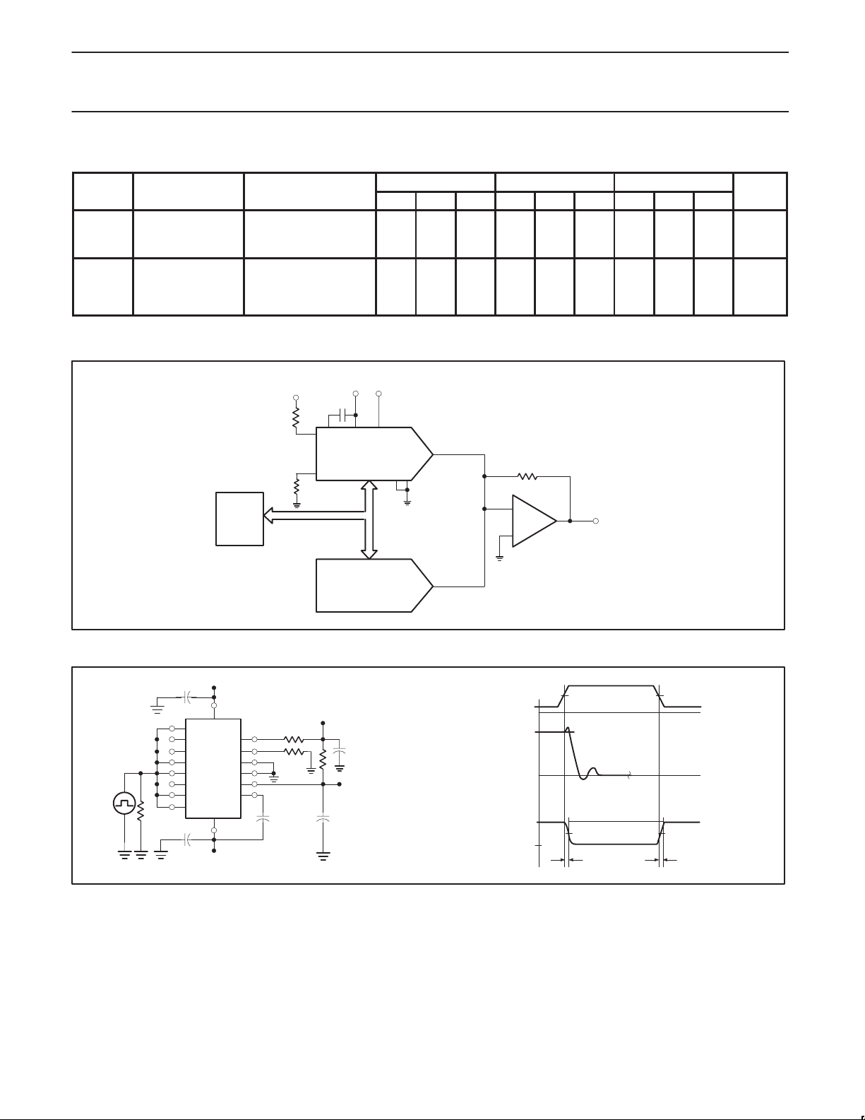
TEST CIRCUITS
Settling time
switched on or off,
T
= 25 °C
amb
70 135 70 135 70 135 ns
Propagation delay
Low-to-High T
= 25 °C, each bit. ns
amb
High-to-Low All bits switched 35 60 35 60 35 60
V– V+
16
14
15 5-12 1 2
ACCURACY > 0.006%
133
DAC-08
REFERENCE DAC
4
R
f
–
NE5534
+
ERROR
OUTPUT
SL00003
CONTROL
LOGIC
R
REF
R15
V
REF
Figure 3. Relative Accuracy Test Circuit
V
CC
0.1 µF
13
5
6
7
8
DAC-08
9
10
11
e
IN
51 Ω
12
0.1 µF
14
15
1
2
4
16
3
V
EE
15 pF
1.0 kΩ
1.0 kΩ
+2.0 V
R
DC
0.1 µF
L
FOR SETTLING TIME
MEASUREMENT
(ALL BITS
e
O
SWITCHED LOW
TO HIGH)
CO ≤ 25 pF
SETTLING TIME
e
IN
= 500 Ω
R
L
TRANSIENT
RESPONSE
-100 mV
2.4 V
0.4 V
1.0 V
1.4 V
t
= t
PHL
0
0
= 10 ns
PLH
= 70 ns TYPICAL
t
S
TO ±1/2 LSB
t
PLH
to GND
USE R
L
FOR TURN OFF
MEASUREMENT
RL = 50 Ω
PIN 4 TO GND
t
PHL
SL00004
Figure 4. Transient Response and Settling Time
2001 Aug 03
6
Page 7

Philips Semiconductors Product data
DAC-08 Series8-bit high-speed multiplying D/A converter
TEST CIRCUITS (Continued)
V
CC
R
13
5
6
7
8
DAC-08
9
10
11
12
0.1 µF
3
V
EE
14
15
1
2
4
16
REQ = 200 Ω
OPEN
IN
1 kΩ
R
P
R
L
SCOPE
V
IN
dI
dV
I
+
R
dt
dt
L
Figure 5. Reference Current Slew Rate Measurement
2V
0
10%
90%
SLEWING TIME
0
2.0 mA
SL00005
V
CC
I
CC
13
5
A
1
6
A
2
7
A
3
8
A
DIGITAL
INPUTS
NOTES:
(See text for values of C.)
Typical values of R14 = R15 = 1 kΩ
and II apply to inputs A1 through A
V
I
The resistor tied to Pin 15 is to temperature compensate the bias current and may not be necessary for all applications.
A
1
IO+ K
Ť
2
where K [
and AN = ‘1’ if AN is at High Level
= ‘0’ if AN is at Low Level
A
N
V
R
)
REF
14
V
REF
C = 15 pF
A
2
)
4
= +2.0 V
A
3
)
8
8
A
A
5
4
)
)
32
16
4
A
5
A
6
A
7
A
8
(+)
V
I
A
A
6
7
)
64
128
DAC-08
9
10
11
12
I
I
3
I
EE
V
EE
A
8
)
Ť
256
I
14
R
14
15
1
2
4
16
14
I
15
R
15
I
O
C
R
V
V
OUTPUT
L
SL00006
Figure 6. Notation Definitions
O
REF
(+)
2001 Aug 03
7
Page 8

Philips Semiconductors Product data
DAC-08 Series8-bit high-speed multiplying D/A converter
TYPICAL PERFORMANCE CHARACTERISTICS
Output Current vs Output Voltage
(Output Voltage Compliance)
3.2
2.8
2.4
V– = –15V V– = –5V
2.0
1.6
1.2
0.8
OUTPUT CURRENT (mA)
0.4
0
–14 –10 –6 –2 0 2 6 10 14 18
ALL BITS ON
TA = T
OUTPUT VOLTAGE (V)
Full-Scale Settling Time LSB Switching
ALL BITS SWITCHED ON
2.4V
OUTPUT – 1/2LSB
SETTLING +1/2LSB
0.4V
0
50ns/DIVISIOM
=2mA, RL=1kΩ 1/2LSB=4µA
I
FS
min
TO T
I
REF
I
REF
I
REF
= 0.2mA
max
= 2mA
= 1mA
Fast Pulsed Reference Operation
2.5V
V
IN
0.5V
–0.5mA
I
OUT
–2.5mA
200ns/division
= 200Ω, RL = 100Ω, CC = 0
R
EQ
2.4V
BIT 8
LOGIC
INPUT
0.4V
0V
8µA
I
OUT
0
50ns/DIVISIOM
True and Complementary Output
Operation
0mA
1.0mA
2.0mA
(00000000) (11111111)
Full-Scale Current vs
Reference Current
5.0
TA = T
ALL BITS “HIGH”
4.0
3.0
2.0
1.0
FS
I – OUTPUT CURRENT (mA)
0
0 1.0 2.0 3.0 4.0 5.0
TO T
min
max
I
— REFERENCE CURRENT (mA)
REF
LIMIT FOR
V–=–15V
LIMIT FOR
V–=–5V
I
OUT
I
OUT
LSB Propagation Delay vs IFS
500
400
300
200
100
PROPAGATION DELAY (ns)
1LSB=78nA
0
I
.05
.01
— OUTPUT FULL SCALE CURRENT (mA)
FS
.02
.05
1LSB=7.8µA
0.1
0.2
0.5
1.0
Reference Input Frequency Response
6
4
2
0
–2
–4
–6
R14=R15=1kΩ
–8
RL ≤ 500Ω
–10
ALL BITS “ON”
RELATIVE OUTPUT (dB)
VR15 = 0V
–12
–14
2.0
5.0
10
0.1 0.2 0.5 1.0 2.0 5.0
NOTES:
Curve 1: CC = 15pF, V
Curve 1: CC = 15pF, V
Curve 1: CC = 15pF, V
FREQUENCY (MHz)
IN
IN
and applied through 50Ω connected to Pin 14.
+2.0V applied to R
IN
Figure 7. Typical Performance Characteristics
3
= 2.0V
P-P
= 5m0V
= 100m0V
.
14
1
2
centered at +1.0V
centered at +200mV
P-P
centered at 0V
P-P
10
SL00007
2001 Aug 03
8
Page 9

Philips Semiconductors Product data
DAC-08 Series8-bit high-speed multiplying D/A converter
TYPICAL PERFORMANCE CHARACTERISTICS (Continued)
Reference AMP Common-Mode Range
All Bits On
3.2
2.8
2.4
2.0
1.6
1.2
0.8
0.4
OUTPUT CURRENT (mA)
0
–14 –10 –6 –2 0 2 6 10 14 18
— REFERENCE COMMON MODE VOLTAGE (V)
V
15
POSITIVE COMMON-MODE RANGE IS ALWAYS (V+) –1.5V.
TA = T
to T
MIN
MAX
V– = –15V V– = –5V V+ = +5V
I
= 2mA
REF
I
= 1mA
REF
I
= 0.2mA
REF
Output Voltage Compliance
vs Temperature
20
16
12
8
4
0
OUTPUT VOLTAGE (V)
–4
–8
–12
Shaded area indicates
permissible output voltage
range for V– = -15V, I
For other V– or I
See “Output Current vs Output
Voltage” curve on previous page
–50 0 50 100 150
TEMPERATURE (°C)
REF
≤ 2.0mA
REF
Logic Input Current vs Input Voltage V
8.0
µ
6.0
4.0
2.0
LOGIC INPUT CURRENT ( A)
0
–12 –8 –4 0 4 8 12 16
LOGIC INPUT VOLTAGE (V)
– VLC vs Temperature
TH
2.0
1.8
1.6
1.4
1.2
1.o
0.8
THLC
V – V (V)
0.6
0.4
0.2
0
–50 0 50 100 150
TEMPERATURE (°C)
Bit Transfer Characteristics Power Supply Current vs V+
1.4
1.2
I
= 2.0mA
REF
1.0
0.8
0.6
0.4
OUTPUT CURRENT (mA)
V– = –15V
0.2
V– = –5V
0
–12 –8 –4 0 4 8 12 16
LOGIC INPUT VOLTAGE (V)
NOTES:
B
through B8 have identical transfer characteristics.
1
Bits are fully switched, with less than 1/2LSB error, at
less than ±100mV from actual threshold. These
switching points are guaranteed to lie between 0.8 and
2.0V over the operating temperature range
(VLC = 0.0V).
B
1
B
2
B
3
B
4
B
5
8
ALL BITS HIGH OR LOW
7
6
5
4
3
2
1
POWER SUPPLY CURRENT (mA)
0
–50 0 50 100 150
V+ – POSITIVE POWER SUPPLY (V
I–
I+
)
DC
Power Supply Current vs V– Power Supply Current vs Temperature
8
7
6
5
4
3
2
1
POWER SUPPLY CURRENT (mA)
0
V– — NEGATIVE POWER SUPPLY (V
2001 Aug 03
BITS MAY BE HIGH OR LOW
I– WITH I
I– WITH I
I– WITH I
0 –4.0 –8.0 –12 –16 –20
REF
REF
REF
= 2mA
= 1mA
= 0.2mA
I+
DC
)
8
BITS MAY BE HIGH OR LOW
POWER SUPPLY CURRENT (mA)
7
6
5
4
3
2
1
0
V– = +15V
I
= 2.0mA
REF
V+ = +15V
–50 0 50 100 150
TEMPERATURE (°C)
I–
I+
Figure 8. Typical Performance Characteristics (cont.)
9
Maximum Reference Input Frequency
vs Compensation Capacitor Value
10,000
1,000
MAX
F (kHz)
100
10
1
10
100
(pF)
C
C
1000
SL00008
Page 10

Philips Semiconductors Product data
DAC-08 Series8-bit high-speed multiplying D/A converter
TYPICAL APPLICATION
+V
REF
OPTIONAL RESISTOR
FOR OFFSET
R
0V
NOTES:
REQ = R
Typical Values
= 5kΩ
R
IN
= 10V
+V
IN
Pulsed Referenced Operation
INPUTS
IN
R
REF
14
15
16
NO CAP
4
2
SL00009
REQ
=200Ω
R
P
|| R
IN
P
Figure 9. Typical Application
FUNCTIONAL DESCRIPTION
Reference Amplifier Drive and Compensation
The reference amplifier input current must always flow into Pin 14
regardless of the setup method or reference supply voltage polarity.
Connections for a positive reference voltage are shown in Figure 3.
The reference voltage source supplies the full reference current. For
bipolar reference signals, as in the multiplying mode, R
tied to a negative voltage corresponding to the minimum input level.
R
may be eliminated with only a small sacrifice in accuracy and
15
temperature drift.
The compensation capacitor value must be increased as R
is increased. This is in order to maintain proper phase margin. For
R
values of 1.0, 2.5, and 5.0 kΩ, minimum capacitor values are
14
15, 37, and 75 pF, respectively. The capacitor may be tied to either
V
or ground, but using VEE increases negative supply rejection.
EE
(Fluctuations in the negative supply have more effect on accuracy
than do any changes in the positive supply.)
A negative reference voltage may be used if R
the reference voltage is applied to R
15
14
as shown. A high input
impedance is the main advantage of this method. The negative
reference voltage must be at least 3.0 V above the V
Bipolar input signals may be handled by connecting R
reference voltage equal to the peak positive input level at Pin 15.
When using a DC reference voltage, capacitive bypass to ground is
recommended. The 5.0 V logic supply is not recommended as a
reference voltage, but if a well regulated 5.0V supply which drives
logic is to be used as the reference, R
should be formed of two
14
series resistors with the junction of the two resistors bypassed with
0.1 µF to ground. For reference voltages greater than 5.0 V, a clamp
diode is recommended between Pin 14 and ground.
If Pin 14 is driven by a high impedance such as a transistor current
source, none of the above compensation methods applies and the
amplifier must be heavily compensated, decreasing the overall
bandwidth.
can be
15
value
14
is grounded and
supply.
EE
to a positive
14
Output V oltage Range
The voltage at Pin 4 must always be at least 4.5 V more positive
than the voltage of the negative supply (Pin 3) when the reference
current is 2 mA or less, and at least 8 V more positive than the
negative supply when the reference current is between 2 mA and
4 mA. This is necessary to avoid saturation of the output transistors,
which would cause serious accuracy degradation.
Output Current Range
Any time the full-scale current exceeds 2 mA, the negative supply
must be at least 8 V more negative than the output voltage. This is
due to the increased internal voltage drops between the negative
supply and the outputs with higher reference currents.
Accuracy
Absolute accuracy is the measure of each output current level with
respect to its intended value, and is dependent upon relative
accuracy, full-scale accuracy and full-scale current drift. Relative
accuracy is the measure of each output current level as a fraction of
the full-scale current after zero-scale current has been nulled out.
The relative accuracy of the DAC-08 series is essentially constant
over the operating temperature range due to the excellent
temperature tracking of the monolithic resistor ladder. The reference
current may drift with temperature, causing a change in the absolute
accuracy of output current. However, the DAC-08 series has a very
low full-scale current drift over the operating temperature range.
The DAC-08 series is guaranteed accurate to within ± LSB at
+25 °C at a full-scale output current of 1.992 mA. The relative
accuracy test circuit is shown in Figure 3. The 12-bit converter is
calibrated to a full-scale output current of 1.99219 mA, then the
DAC-08 full-scale current is trimmed to the same value with R
so
14
that a zero value appears at the error amplifier output. The counter
is activated and the error band may be displayed on the
oscilloscope, detected by comparators, or stored in a peak detector.
Two 8-bit D-to-A converters may not be used to construct a 16-bit
accurate D-to-A converter. 16-bit accuracy implies a total of ± part in
65,536, or ±0.00076%, which is much more accurate than the
±0.19% specification of the DAC-08 series.
Monotonicity
A monotonic converter is one which always provides analog output
greater than or equal to the preceding value for a corresponding
increment in the digital input code. The DAC-08 series is monotonic
for all values of reference current above 0.5 mA. The recommended
range for operation is a DC reference current between 0.5 mA and
4.0 mA.
Settling Time
The worst-case switching condition occurs when all bits are
switched on, which corresponds to a low-to-high transition for all
input bits. This time is typically 70 ns for settling to within LSB for
8-bit accuracy. This time applies when R
The slowest single switch is the least significant bit, which typically
turns on and settles in 65 ns. In applications where the DAC
functions in a positive-going ramp mode, the worst-case condition
does not occur and settling times less than 70 ns may be realized.
Extra care must be taken in board layout since this usually is the
dominant factor in satisfactory test results when measuring settling
time. Short leads, 100 µF supply bypassing for low frequencies,
minimum scope lead length, and avoidance of ground loops are all
mandatory .
<500 Ω and CO<25 pF.
L
2001 Aug 03
10
Page 11

Philips Semiconductors Product data
DAC-08 Series8-bit high-speed multiplying D/A converter
SETTLING TIME AND PROPAGATION DELAY
VS + = +15V
V
IN
Q
1
R1 = 1000Ω
R
= 5kΩ
V
= 10V
REF
14
= 2mA
I
REF
R
= 5kΩ
15
14
15
DUT
12111098765
16 3 1
C
C
1
2
4
2
C
5
V
OUT
50Ω
R
D
= 1000Ω
2
1
D
C
3
V
ADJ
D
3
V
OUT
R
= 500Ω
3
C
4
2
NOTES:
, D2 = IN6263 or equivalent
D
1
D
= IN914 or equivalent
3
C1 = 0.01µF
C
, C3 = 0.1µF
2
= 2N3904
Q
1
, C5 = 15pF and includes all probe and fixturing capacitance.
C
4
BASIC DAC-08 CONFIGURATION
R
REF
(LOW T.C.)
VS – = –15V
Figure 10. Settling Time and Propagation Delay
+V
REF
I
REF
MSB 2 3 4 5 6 7 LSB
56789101112
14
15
DAC-08
316
13
4
2
1
I
I
SL00010
O
O
NOTES:
I
FS
2001 Aug 03
V–
0.1µF
V
R
REF
REF
255
x
;IO IO IFSfor all logic states
256
C
COMP
V+
0.1µF
SL00011
Figure 11. Basic DAC-08 Configuration
11
Page 12

Philips Semiconductors Product data
DAC-08 Series8-bit high-speed multiplying D/A converter
RECOMMENDED FULL-SCALE AND ZERO-SCALE ADJUST
V
REF
R
1
R
2
NOTES:
R
= low T.C.
1
= R1 + R
R
3
R2 ≈ 0.1 R1 to minimize pot. contribution to full-scale drift
2
14
15
R
3
DAC-08
4
2
Figure 12. Recommended Full-Scale and Zero-Scale Adjust
UNIPOLAR VOLTAGE OUTPUT FOR LOW IMPEDANCE OUTPUT
IR = 2mA
14
15
DAC-08
4
2
5kΩ
= 1MΩ
R
4
SL00012
V
OUT
V–
=
V+
R
= 20kΩ
S
5kΩ (LOW T .C.)
–
NE531
OR
EQUIV 0 TO +10V
+
2001 Aug 03
SL00013
Figure 13. Unipolar Voltage Output for Low Impedance Output
12
Page 13

Philips Semiconductors Product data
DAC-08 Series8-bit high-speed multiplying D/A converter
UNIPOLAR VOLTAGE OUTPUT FOR HIGH IMPEDANCE OUTPUT
V = 10V
5kΩ 5kΩ
V
OUT
V
OUT
IR = 2mA
DAC-08
14
4
2
a. Positive Output
V
OUT
IR = 2mA
DAC-08
14
a. Negative Output
Figure 14. Unipolar Voltage Output for High Impedance Output
BASIC BIPOLAR OUTPUT OPERATION (OFFSET BINARY)
IR = 2mA
Positive full-scale
Positive FS – 1LSB
+ Zero-scale + 1LSB
Zero-scale
Zero-scale – 1LSB
Negative full scale – 1LSB
Negative full scale
Figure 15. Basic Bipolar Output Operation (Offset Binary)
DAC-08
14
B
1B2B3B4B5B6B7B8
1
1
1
1
1
1
1
0
1
0
0
0
0
0
0
1
1
0
0
0
0
4
2
1
1
1
1
0
0
0
0
1
1
0
0
0
0
4
2
V
OUT
SL00014
V = 10V
10kΩ
10kΩ
V
OUT
V
OUT
V
OUT
1
1
1
–9.920V
1
1
0
–9.840V
0
0
1
0
0
1
1
0
0
0
0
–0.080V
0
0.000
1
0.080
1
+9.920
0
+10.000
V
OUT
+10.000
+9.920
+0.160
+0.080
0.000
–9.840
–9.920
SL00015
2001 Aug 03
13
Page 14

Philips Semiconductors Product data
DAC-08 Series8-bit high-speed multiplying D/A converter
DIP16: plastic dual in-line package; 16 leads (300 mil) SOT38-4
2001 Aug 03
14
Page 15

Philips Semiconductors Product data
DAC-08 Series8-bit high-speed multiplying D/A converter
SO16: plastic small outline package; 16 leads; body width 3.9 mm SOT109-1
2001 Aug 03
15
Page 16

Philips Semiconductors Product data
DAC-08 Series8-bit high-speed multiplying D/A converter
Data sheet status
Product
Data sheet status
Objective data
Preliminary data
Product data
[1] Please consult the most recently issued data sheet before initiating or completing a design.
[2] The product status of the device(s) described in this data sheet may have changed since this data sheet was published. The latest information is available on the Internet at URL
http://www.semiconductors.philips.com.
[1]
status
Development
Qualification
Production
[2]
Definitions
Short-form specification — The data in a short-form specification is extracted from a full data sheet with the same type number and title. For
detailed information see the relevant data sheet or data handbook.
Limiting values definition — Limiting values given are in accordance with the Absolute Maximum Rating System (IEC 60134). Stress above one
or more of the limiting values may cause permanent damage to the device. These are stress ratings only and operation of the device at these or
at any other conditions above those given in the Characteristics sections of the specification is not implied. Exposure to limiting values for extended
periods may affect device reliability.
Application information — Applications that are described herein for any of these products are for illustrative purposes only. Philips
Semiconductors make no representation or warranty that such applications will be suitable for the specified use without further testing or
modification.
Disclaimers
Life support — These products are not designed for use in life support appliances, devices or systems where malfunction of these products can
reasonably be expected to result in personal injury . Philips Semiconductors customers using or selling these products for use in such applications
do so at their own risk and agree to fully indemnify Philips Semiconductors for any damages resulting from such application.
Right to make changes — Philips Semiconductors reserves the right to make changes, without notice, in the products, including circuits, standard
cells, and/or software, described or contained herein in order to improve design and/or performance. Philips Semiconductors assumes no
responsibility or liability for the use of any of these products, conveys no license or title under any patent, copyright, or mask work right to these
products, and makes no representations or warranties that these products are free from patent, copyright, or mask work right infringement, unless
otherwise specified.
Contact information
For additional information please visit
http://www.semiconductors.philips.com . Fax: +31 40 27 24825
For sales offices addresses send e-mail to:
sales.addresses@www.semiconductors.philips.com.
Definitions
This data sheet contains data from the objective specification for product development.
Philips Semiconductors reserves the right to change the specification in any manner without notice.
This data sheet contains data from the preliminary specification. Supplementary data will be
published at a later date. Philips Semiconductors reserves the right to change the specification
without notice, in order to improve the design and supply the best possible product.
This data sheet contains data from the product specification. Philips Semiconductors reserves the
right to make changes at any time in order to improve the design, manufacturing and supply.
Changes will be communicated according to the Customer Product/Process Change Notification
(CPCN) procedure SNW-SQ-650A.
Koninklijke Philips Electronics N.V. 2001
All rights reserved. Printed in U.S.A.
Date of release: 10-01
Document order number: 9397 750 08922
2001 Aug 03
16
Page 17

This datasheet has been download from:
www.datasheetcatalog.com
Datasheets for electronics components.
 Loading...