

Page 1

Philips Semiconductors
Interconnectivity
D12 SMART
USER’S
MANUAL
Philips Semiconductors - Asia Product Innovation Centre
Visit http://www.flexiusb.com
Page 2

USER’S MANUAL D12 SMART Page 2 of 19
TABLE OF CONTENTS
D12 SMART KIT.......................................................................................... 3
1.1 Introduction.............................................................................................. 3
1.2 Description .............................................................................................. 3
1.3 Features ................................................................................................... 3
1.4 Operating Environment ............................................................................ 3
2. SETTING UP THE D12 SMART KIT..................................................... 3
2.1 Connection and System Requirement ....................................................... 3
2.1.1: The D12 Smart Evaluation System ................................................... 4
2.1.2: Block Diagram of D12 Smart Board.................................................. 4
3. INSTALLATION PROCEDURES........................................................... 5
3.1 Installing the software.............................................................................. 5
3.2 Installing the Applet................................................................................. 5
3.2.1: The icon on the desktop.................................................................... 5
3.3 Installing the device drivers...................................................................... 5
3.4 Running the applet ................................................................................... 7
4. DESCRIPTION OF D12 ENDPOINTS.................................................... 8
4.1 D12 Endpoints Configuration................................................................... 8
4.1.1 Configuration of D12 Endpoints Table ............................................... 8
4.2 Operations of D12 Endpoints................................................................... 8
4.2.1 Operations of D12 Endpoints Table .................................................... 8
5. MISCELLANEOUS................................................................................. 9
6. DESCRIPTION OF HEADERS..............................................................10
6.1 Header J1 ................................................................................................10
6.2 Header J2 ................................................................................................10
6.3 Header J3 ................................................................................................12
6.4 Header J4 (USB Upstream).....................................................................13
9. PCB PLOTS OF D12 SMART EVALUATION BOARD........................16
10. D12 SMART EVALUATION BOARD................................................18
10.1: Enlarged Picture of PDIUSBD12.......................................................18
11. BILL OF MATERIALS FOR D12 EVALUATION BOARD ...............19
_________________________________________________________________________________________________________
Philips Semiconductors - Asia Product Innovation Centre
Visit http://www.flexiusb.com
Page 3

USER’S MANUAL D12 SMART Page 3 of 19
D12 SMART KIT
1.1 Introduction
The Philips USB D12 Smart Kit is a comprehensive kit that offers you the full potential of Philips
PDIUSBD12 (or D12), in addition to the know-how on how to convert your existing legacy into
USB devices. This kit includes the D12 smart boards, test application program (or applet), USB
driver, and some sample firmware source codes.
1.2 Description
D12 is a high performance USB interface device that offers DMA transfer capability as well as
features for a cost-effective microcontroller-based system. This kit allows you to thoroughly
evaluate the capabilities and features of the device, and provide quick grounding on how to
convert your existing non-USB devices such as the digital still camera, mass storage device, and
scanner into USB devices.
1.3 Features
The simple design of this kit aims to highlight the features of a USB device. It has the D12 and
the 89C738/89C52 microcontroller interfaced to D12. Philips PDIUSBD12 implements all the
functions of the USB device, and has an 8-bit parallel data bus for microcontroller interface. The
MCU is a member of the 8051-family. The firmware implements all the USB enumeration, D12
Interrupt service, power down and resume signaling interfaces. Though the D12 has DMA
capability, for simplicity, it is not incorporated in this board. A similar evaluation board, the USBEPP, has all the DMA features built into it.
With the accompanying applet, you can operate the kit in three modes: Print, Scan, and Loop
back modes. The purpose for having the print and scan modes is to allow the evaluation board to
emulate either the printer or scanner environment. The Loop back mode is to indicate the integrity
of the data when large data packet is sent and received from the host system.
1.4 Operating Environment
Running the kit only requires a new generation PC (motherboard with USB port) with Microsoft
Windows 98 operating system. The firmware provided with the kit is written in C language (some
Assembly codes for critical timing), and so allows you to port it to any other platforms for
compiling. With this kit, you can develop your USB devices through the firmware and hardware
schematics.
2. SETTING UP THE D12 SMART KIT
2.1 Connection and System Requirement
Connect the board to the host system via the USB upstream connector. Follow the instructions on
the screen to install the device driver, and then install the software provided with the kit. Ensure
that you have the following:
_________________________________________________________________________________________________________
Philips Semiconductors - Asia Product Innovation Centre
Visit http://www.flexiusb.com
Page 4

USER’S MANUAL D12 SMART Page 4 of 19
Mouse
D12
MCU Exbus
Serial Port
D12 Exbus
USB Cable
• PC Host system with USB ports;
• Microsoft Windows 98 operating system; and
• D12 smart board, USB cable, and diskette provided with the kit.
2.1.1: The D12 Smart Evaluation System
D12 Board
MCU
Host PC with USB host Controller
The Evaluation System based on USB D12 Kit
2.1.2: Block Diagram of D12 Smart Board
D12
MCU
Suspend & Resume
Circuitry
USB
_________________________________________________________________________________________________________
Philips Semiconductors - Asia Product Innovation Centre
Visit http://www.flexiusb.com
Page 5

USER’S MANUAL D12 SMART Page 5 of 19
3. INSTALLATION PROCEDURES
3.1 Installing the software
The software includes the firmware, the test application program (or the applet), and the device
drivers. The firmware is programmed in the 89C738/89C52 microcontroller (Flash type). If you
want to change the firmware or use your own firmware, you just need to reprogram the
89C738/89C52 microcontroller.
3.2 Installing the Applet
1. Insert the diskette into your disk drive.
2. Copy the file, D12TEST.EXE, contained in the diskette to a directory of your choice -
C:\D12 Smart.
3. Create a shortcut by dragging the file D12TEST.EXE from the directory to the desktop. An
icon similar to Figure 3.2.1 appears.
3.2.1: The icon on the desktop.
3.3 Installing the device drivers
When connecting the USB cable to your host system for the first time, a dialog box will appear
and prompt you to install the device drivers. Navigate through it and load the device drivers
provided in the floppy that comes along with the kit. To install the device drivers:
1. When you connect the USB cable to your host system for the first time, a dialog box
similar to Figure 3.3.1 appears. Click the Next button.
Figure 3.3.1
_________________________________________________________________________________________________________
Philips Semiconductors - Asia Product Innovation Centre
Visit http://www.flexiusb.com
Page 6
USER’S MANUAL D12 SMART Page 6 of 19
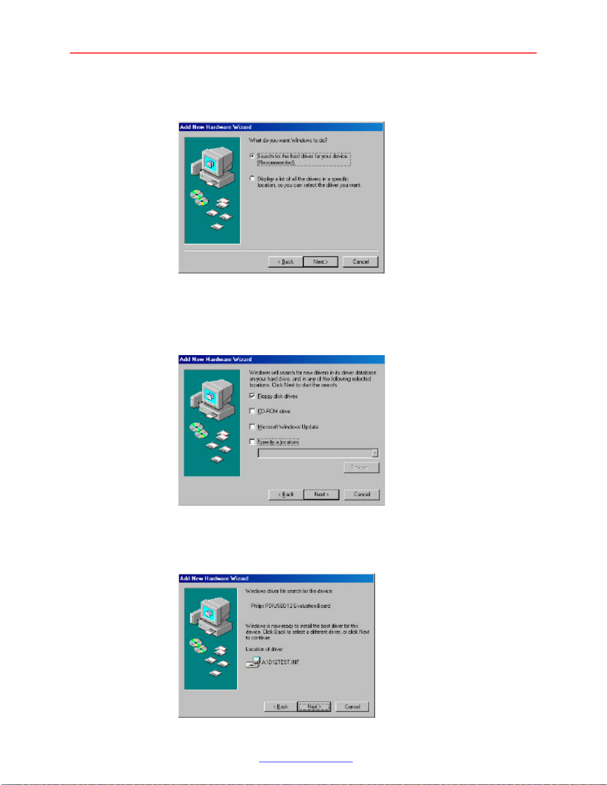
2. When a dialog box similar to Figure 3.3.2 appears, select the first item and click the Next
button.
Figure 3.3.2
3. When a dialog box similar to Figure 3.3.3 appears, select Floppy disk drives and click the
Next button.
Figure 3.3.3
4. When a dialog box similar to Figure 3.3.4 appears, click the Next button.
Figure 3.3.4
_________________________________________________________________________________________________________
Philips Semiconductors - Asia Product Innovation Centre
Visit http://www.flexiusb.com
Page 7

USER’S MANUAL D12 SMART Page 7 of 19
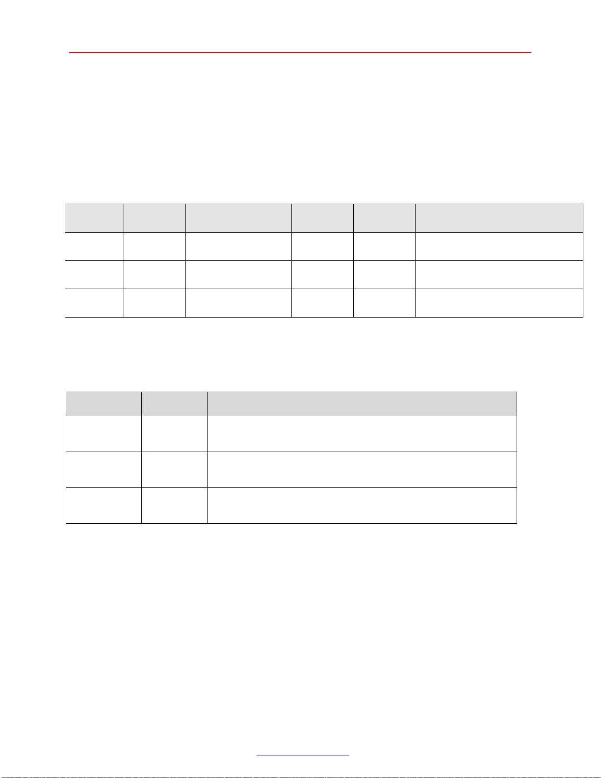
5. When a dialog box similar to Figure 3.3.5 appears, click the Finish button to end the
installation.
Figure 3.3.5
3.4 Running the applet
The applet supports three test modes: Print, Scan, and Loop back modes. The print and scan
modes allow the evaluation board to emulate either the printer or scanner environment. The Loop
back mode shows the integrity of the data when a large data packet is sent and received by the
host system.
To run the applet, click the D12Test.exe icon on your desktop and an interface similar to Figure
3.4.1 appears.
Figure 3.4.1
_________________________________________________________________________________________________________
Philips Semiconductors - Asia Product Innovation Centre
Visit http://www.flexiusb.com
Page 8
USER’S MANUAL D12 SMART Page 8 of 19
This pipe is defined as Interrupt pipe. The D12-Smart
evaluation board sends specific data packet to the host system
This pipe is defined as Bulk Out pipe. Data packet received
from the host system is interpreted as LED control, and the
These pipes are defined as Bulk In/Out endpoints. The Applet
and the evaluation board support 3 test modes: loop back,
4. DESCRIPTION OF D12 ENDPOINTS
4.1 D12 Endpoints Configuration
Table 4.1.1 describes the PDIUSBD12 Endpoints configuration Mode 0, i.e., it is Non-Iso mode.
The reset 3 mode (Isochronous mode ) can be found on the D12 specification.
4.1.1 Configuration of D12 Endpoints Table
Endpoint
Number
0 0
1 2
2 4
Endpoint
Index
1
3
5
Transfer
Type
Control Out
Control In
Generic Out
Generic In
Generic(Main) Out
Generic(Main) In
Endpoint
Direction Max Packet Size(Bytes)
Type
Default Out
In
Generic
Generic
Generic
Generic
Out
In
Out
In
16
16
16
16
64(another 64 for double buffer)
64(another 64 for double buffer)
4.2 Operations of D12 Endpoints
The table below describes in detail the operations of the endpoints.
4.2.1 Operations of D12 Endpoints Table
Endpoint
Number
Endpoint
Type
Operations
1 Generic In
when the test key is pressed or released.
1 Generic
Out
firmware will light up the corresponding LED.
2 Main In
Main Out
print, and scan modes.
The Generic In and Generic Out endpoints have a maximal packet size of 16 bytes. This
capacity makes them suitable for devices that require small size data transfer such as the
keyboard, mouse and logic controls. The main endpoints have a maximal packet size of 64
bytes for Bulk/Isochronous mode or 128 bytes for Isochronous mode with double buffering
capacity. Hence, they are suitable for high data rate and large size data transfer.
Three test modes are supported at the main endpoints. They are:
• Scan mode: The evaluation board emulates the scanner environment. This mode is used
to evaluate the maximal Bulk In transfer rate.
• Print mode: The evaluation board emulates the printer environment. This mode is used
to evaluate the maximal Bulk Out transfer rate.
• Loop back mode: The evaluation board receives data packets from the Main Out
endpoint (Endpoint Index 4) and sends them back to the host system from the Main In
endpoint (Endpoint Index 5). This mode helps test the firmware’s ability to control the
_________________________________________________________________________________________________________
Philips Semiconductors - Asia Product Innovation Centre
Visit http://www.flexiusb.com
Page 9

USER’S MANUAL D12 SMART Page 9 of 19
data flow and the integrity of data transfers.
Since the firmware is protocol-based, the host system can inform the firmware to set any
possible modes. There is, therefore, no longer any need to manually set the scan test mode
before running the scan test on the firmware.
The “buffer size” of the applet is the size of the data buffer, which the applet transmits to the
USB system drivers for receiving or transmitting. Hence, it is the responsibility of the USB
system drivers to divide them into smaller data packets, e.g., 64 bytes for bulk transfer. The
maximal buffer size is limited by the USB system drivers. The best transfer rate over the USB
can be achieved by optimizing the buffer size.
5. MISCELLANEOUS
• Press-Button S1—Reset or Resume the system
• Press-Button S2—PIPE testing
• Press-Button S3—PIPE testing
• LED D1—USB interface GoodLink indicator. When it is on, it means that the link between
the USB host and the USB device has been set up and the enumeration done. If it is blinking,
it means that data is being transmitted or received
• LED D2—PIPE testing
• LED D3—PIPE testing
• Header pin J5 —Connected to Ground leads
• HCT123 with D12 and MCU firmware support the Power down and RESUME operations,
i.e., when D12 comes out from suspend state, the suspend pin state changes from high to low.
When this happens, the HCT123 monostate generates a positive pulse to reset/wakeup
89C52/89C738.
_________________________________________________________________________________________________________
Philips Semiconductors - Asia Product Innovation Centre
Visit http://www.flexiusb.com
Page 10

USER’S MANUAL D12 SMART Page 10 of 19
6. DESCRIPTION OF HEADERS
6.1 Header J1
The J1 test header is for D12’s signals as illustrated in the following table:
Pin No. Signal Name Signal Type Description
1
2
D∅
D12A∅
I/O
I
D12 Data ∅
D12 Address A∅
3 D1 I/O D12 Data 1
4 /D12RST I D12 Reset
5 D2 I/O D12 Data 2
6 /D12 EOT I D12 End of Transfer
7 D3 I/O D12 Data 3
8 /D12DACK I D12 DMA ACK
9 D4 I/O D12 Data 4
10 D12REQ O D12 DMA Request
11 D5 I/O D12 Data 5
12 /D12WR I D12 Write
13 D6 I/O D12 Data 6
14 /D12RD I D12 Read
15 D7 I/O D12 Data 7
16 /D12CS I D12 Chip Select
17 5V Power 5 Volts Power
18 D12ALE I D12 Address Catch
19 5V Power 5 volts Power
20 D12SUSPD I/O D12 Suspend
21 Not Connected
22 /D12INT O D12 Interrupt
23 GND Power Ground
24 Not Connected
25 GND Power Ground
26 CLK12M O D12 Clock Out
6.2 Header J2
The expansion connector J2 is connected from Pin1 to Pin 40 of the MCU. These connectors
allow the use of MCUs from other makes through a pin converter. It will also allow you to debug
signal lines of MPU.
_________________________________________________________________________________________________________
Philips Semiconductors - Asia Product Innovation Centre
Visit http://www.flexiusb.com
Page 11

USER’S MANUAL D12 SMART Page 11 of 19
Header J2
Pin No. Signal Name Signal Type Description
1 GND Power Ground
2 SWM0 I
Press Button ∅
3 GND Power Ground
4 SWM1 I Press Button 1
5 GND Power Ground
6 RLED0 O
Red LED ∅
7 GND Power Ground
8 RLED1 O Red LED 1
9 GND Power Ground
10 P1x4 I/O MCU Port 1 bit 4 (Not in use)
11 GND Power Ground
12 P1x5 I/O MCU Port 1 bit 5 (Not in use)
13 GND Power Ground
14 /D12CS I D12 Chip Select
15 GND Power Ground
16 /D12RST O D12 Reset
17 GND Power Ground
18 MCURST I MCU Reset
19 GND Power Ground
20 S232RXD I Receive Data Line
21 GND Power Ground
22 S232TXD O Transmit Data Line
23 GND Power Ground
24 /D12INT I D12 Interrupt
25 GND Power Ground
26 D12 SUSPD I/O D12 Suspend
27 GND Power Ground
28 P3x4 I/O MCU Port 3 bit 4 (Not in use)
29 GND Power Ground
30 P3x5 I/O MCU Port 3 bit 5 (Not in use)
31 GND Power Ground
32 /D12WR O D12 Write
33 GND Power Ground
34 /D12RD O D12 Read
35 GND Power Ground
36 MCUXTAL2 O Crystal Output
37 GND Power Ground
38 MCUXTAL1 I Crystal Input
39 GND Power Ground
40 VCC Power +5V
_________________________________________________________________________________________________________
Philips Semiconductors - Asia Product Innovation Centre
Visit http://www.flexiusb.com
Page 12

USER’S MANUAL D12 SMART Page 12 of 19
6.3 Header J3
Pin No. Signal Name Signal Type Description
1.
2.
3.
4.
5.
6.
7.
8.
9.
10.
11.
12.
13.
14.
15.
16.
17.
18.
19.
20.
21.
22.
23.
24.
25.
26.
27.
28.
29.
30.
31.
32.
33.
34.
35.
36.
37.
38.
39.
40.
VCC Power
GND Power Ground
D0 I/O
GND Power Ground
D1 I/O Data 1
GND Power Ground
D2 I/O Data 2
GND Power Ground
D3 I/O Data 3
GND Power Ground
D4 I/O Data 4
GND Power Ground
D5 I/O Data 5
GND Power Ground
D6 I/O Data 6
GND Power Ground
D7 I/O Data 7
GND Power Ground
/MCUEA O MCU External Excess
GND Power Ground
D12ALE O D12 Address Catch Enable
GND Power Ground
/PSEN O Program Strobe Enable
GND Power Ground
P2x7 I/O MCU Port 2 bit 7 (Not in use)
GND Power Ground
P2x6 I/O MCU Port 2 bit 6 (Not in use)
GND Power
P2x5 I/O MCU Port 2 bit 5 (Not in use)
GND Power Ground
P2x4 I/O MCU Port 2 bit 4 (Not in use)
GND Power Ground
P2x3 I/O MCU Port 2 bit 3 (Not in use)
GND Power Ground
P2x2 I/O MCU Port 2 bit 2 (Not in use)
GND Power Ground
P2x1 I/O MCU Port 2 bit 1 (Not in use)
GND Power Ground
P2x0 I/O MCU Port 2 bit 0 (Not in use)
GND Power Ground
+5V
Data ∅
Ground
_________________________________________________________________________________________________________
Philips Semiconductors - Asia Product Innovation Centre
Visit http://www.flexiusb.com
Page 13

USER’S MANUAL D12 SMART Page 13 of 19
6.4 Header J4 (USB Upstream)
Pin No. Signal Name Signal Type Description
1 V_BUS Power +5V
2 D- I/O Data Minus Line,
3 D+ I/O Data plus Line
4 GND Power Ground
_________________________________________________________________________________________________________
Philips Semiconductors - Asia Product Innovation Centre
Visit http://www.flexiusb.com
Page 14

USER’S MANUAL D12 SMART Page 14 of 19
7. SCHEMATIC OF D12 SMART EVALUATION BOARD
_________________________________________________________________________________________________________
Philips Semiconductors - Asia Product Innovation Centre
Visit http://www.flexiusb.com
Page 15

USER’S MANUAL D12 SMART Page 15 of 19
8. ENLARGED SCHEMATIC OF D12 EXPANSION BUS
_________________________________________________________________________________________________________
Philips Semiconductors - Asia Product Innovation Centre
Visit http://www.flexiusb.com
Page 16

USER’S MANUAL D12 SMART Page 16 of 19
9. PCB PLOTS OF D12 SMART EVALUATION BOARD
Top Layer
Bottom Layer
_________________________________________________________________________________________________________
Philips Semiconductors - Asia Product Innovation Centre
Visit http://www.flexiusb.com
Page 17

USER’S MANUAL D12 SMART Page 17 of 19
..........con’t from pg 18
Top Overlay
_________________________________________________________________________________________________________
Philips Semiconductors - Asia Product Innovation Centre
Visit http://www.flexiusb.com
Page 18

USER’S MANUAL D12 SMART Page 18 of 19
10. D12 SMART EVALUATION BOARD
10.1: Enlarged Picture of PDIUSBD12
_________________________________________________________________________________________________________
Philips Semiconductors - Asia Product Innovation Centre
Visit http://www.flexiusb.com
Page 19

USER’S MANUAL D12 SMART Page 19 of 19
11. BILL OF MATERIALS FOR D12 EVALUATION BOARD
Item Description Reference Value Quantity
1. Capacitor C1, C11, C26, C27, C28 1.0uF16V 5
2. Capacitor
C3, C2
20pF 2
3. Capacitor C4 10uF16V 1
4. Capacitor C5, C17, C18, C19, C20, C21, C22,
0.01uF2KV 11
C23, C31, C32, C33
5. Capacitor C6, C13, C14 4.7uF16V 3
6. Capacitor C7 470pF 1
7. Capacitor C8, C12, C15, C16, C30 0.1uF 5
8. Capacitor C9 68pF 1
9. Capacitor C10 22pF 1
10. Capacitor C24, C25 100pF 2
11. Light Emitting Diode D1 LED_GREEN 1
12. Light Emitting Diode D3, D2 LED_RED 2
13. Jumper J1
HEADER 13×2
1
14. Jumper J2 LEFT Exbus 1
15. Jumper J3 RIGHT Exbus 1
16. Jumper J4 UP_CONN 1
17. Jumper J5 CON1 1
18. Jumper J6 RS232 1
19. Ferrite Bead L1, L2, L3 FERRITE BEAD 3
20. Transistor Q1 2N3906 1
21. Resistor Array RP1 4.7K 1
22. Resistor R2 8.2K 1
23. Resistor R3, R4, R11, R12, R15, R18, R21,
10K 10
R22, R28, R29
24. Resistor R5 1.5K 1
25. Resistor R6, R13, R14 470R 3
26. Resistor R8, R7
18R±1%
2
27. Resistor R9, R10, R16 1M 3
28. Resistor R17, R25 1K 2
29. Resistor R19, R20, R23 0R 3
30. Resistor R24, R26, R27 100K 3
31. Switches S1, S2, S3 PUSHBUTTON 3
32. Integrated Circuit U1 PDIUSBD12_SOP 1
33. Integrated Circuit U2 PDIUSBD12TSSOP 1
34. Integrated Circuit U3 89C738ABP 1
35. Integrated Circuit U4 SN75240 1
36. Integrated Circuit U5 74HCT123 1
37. Crystal X1 6MHz 1
38. Crystal X2 33MHz 1
_________________________________________________________________________________________________________
Philips Semiconductors - Asia Product Innovation Centre
Visit http://www.flexiusb.com
 Loading...