

Philips CR7929 Datasheet

DISCRETE SEMICONDUCTORS
DATA SH EET
book, halfpage
M3D299
CR7929
Triple video driver hybrid amplifier
Preliminary specification 1999 Mar 09
Philips Semiconductors Preliminary specification
Triple video driver hybrid amplifier CR7929
FEATURES
• Transition times (10 to 90%) with 45 V (p-p) swing and
C
=10pF:
L
– rise time (typ.) 2.2 ns
– fall time (typ.) 1.9 ns
• Small 11-pin package
• Design optimized for excellent smearing performance
• Gold metallization for highest reliability.
APPLICATIONS
• Top-end colour cathode-ray tube (CRT) monitors with
pixel frequencies up to 300 MHz.
DESCRIPTION
The CR7929 is a 3-channel hybrid RGB-amplifier module
in an11-pin SOT451A package.
Succeeding the s ucces ful CR6927, C R6928 and CR6929
families, the CR7929 is a pin-compatible next step in
high-bandwidth active load amplifiers. Being an active
load, CR7929 combin es a high bandwi dth with a relativ ely
low and constant dissipation. Its optimized design,
together with innovative application recommendations,
ensures excellent smearing performance.
PINNING
PIN DESCRIPTION
2, 6, 10
4, 8
11
handbook, halfpage
1
input 1
ground
3
5
7
9
output 1
supply voltage (V
input 2
output 2
input 3
)
S
output 3
111
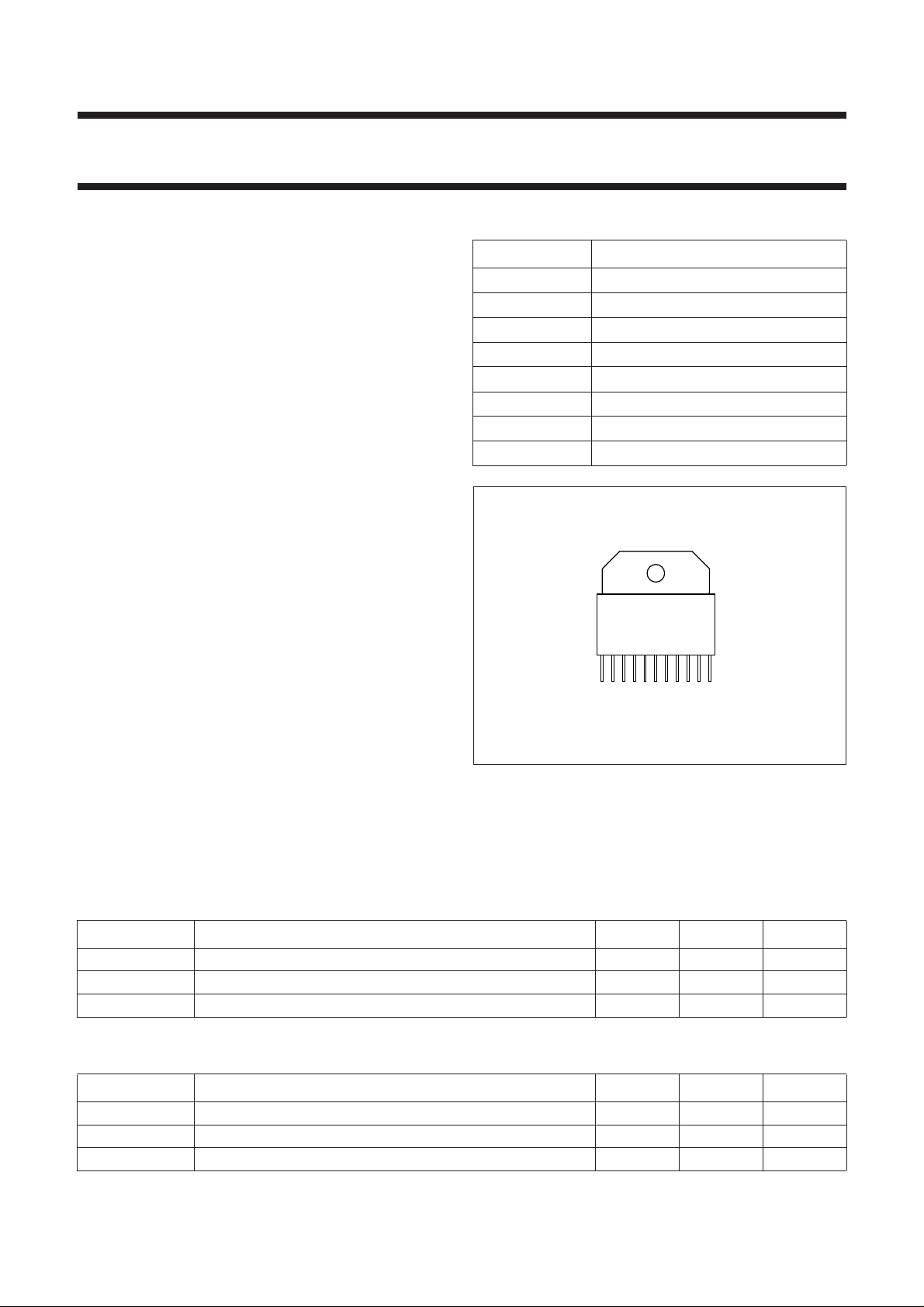
Front view
MBK056
Fig.1 Simplified outline SOT451A.
LIMITING VALUES
In accordance with the Absolute Maximum Rating System (IEC 134).
SYMBOL PARAMETER MIN. MAX. UNIT
V
S
T
mb
T
stg
supply voltage (DC) − 110 V
operating mounting base temperature −20 +100 °C
storage temperature −40 +125 °C
RECOMMENDED OPERATING CONDITIONS
SYMBOL PARAMETER MIN. MAX. UNIT
V
S
T
mb
T
stg
supply voltage (DC) − 90 V
operating mounting base temperature −20 +100 °C
storage temperature −40 +125 °C
1999 Mar 09 2

Philips Semiconductors Preliminary specification
Triple video driver hybrid amplifier CR7929
CHARACTERISTICS
V
=85V; Tmb=25°C; CL= 10 pF; output swing = 45 V (p-p) with 42.5 V DC offset (see Fig.3); unless otherwise
S
specified.
SYMBOL PARAMETER CONDITIONS MIN. TYP. MAX. UNIT
Per amplifier
I
S
P
tot
t
r
t
f
BW small signal bandwidth between −3 dB points; note 2 tbd tbd − MHz
V
os
NLN non-linearity V
A
V
V
G
supply current open input and open output tbd tbd tbd mA
total power dissipation 25 MHz square wave − tbd tbd W
rise time transient response 10 to 90%; note 1 − 2.2 2.7 ns
fall time transient response 10 to 90%; note 1 − 1.9 2.3 ns
overshoot voltag e (rise and fall
time)
adjustable by C1 and C2;
− 810%
see Fig.3
=10to75V − 25%
O
DC voltage gain 50 Ω source; note 3 13.8 15 1 6.2 V/V
insertion gain 50 Ω source; note 4 tbd tbd tbd V/V
Notes
1. Input signal is a 100 kHz square wave of 3.5 V (p-p) with 850 mV DC offset (50 Ω source), without R
2. Sinewave output signal: 1 V (p-p).
3. Measured V
4. Measured V
at input test circuit.
O/VI
at input module.
O/VI
APPLICATION NOTES
1.5 V
150 kΩ680 pF
V
S
output
MDA861
handbook, halfpage
4.3 kΩ
input
level
.
Fig.2 Block diagram, single amplifier.
1999 Mar 09 3
 Loading...