

Page 1

DISCRETE SEMICONDUCTORS
DATA SH EET
ook, halfpage
M3D156
CR6927
Triple video driver hybrid amplifier
Product specification
Supersedes data of 1997 Oct 02
File under Discrete Semiconductors, SC05
1998 Feb 12
Page 2
Philips Semiconductors Product specification
Triple video driver hybrid amplifier CR6927
FEATURES
• Transition times (10 to 90%)
with 45 V (p-p) swing
and CL= 10 pF:
rise time (typ.) 2.5 ns
fall time (typ.) 2.1 ns
• Low power consumption:
11 W with 25 MHz square wave
• Minimum small signal bandwidth:
140 MHz at 1 V (p-p) or
120 MHz at 40 V (p-p)
• Very fast slew rate: 16000 V/µs
• Internal low frequency smearing
compensation
• Excellent grey-scale linearity
• Unconditional stability
• Gold metallization ensures
excellent reliability.
APPLICATIONS
• Cathode-ray tube (CRT) drivers in
high-resolution colour monitors.
DESCRIPTION
Hybrid amplifier module comprising
three video amplifiers in a SOT347
package.
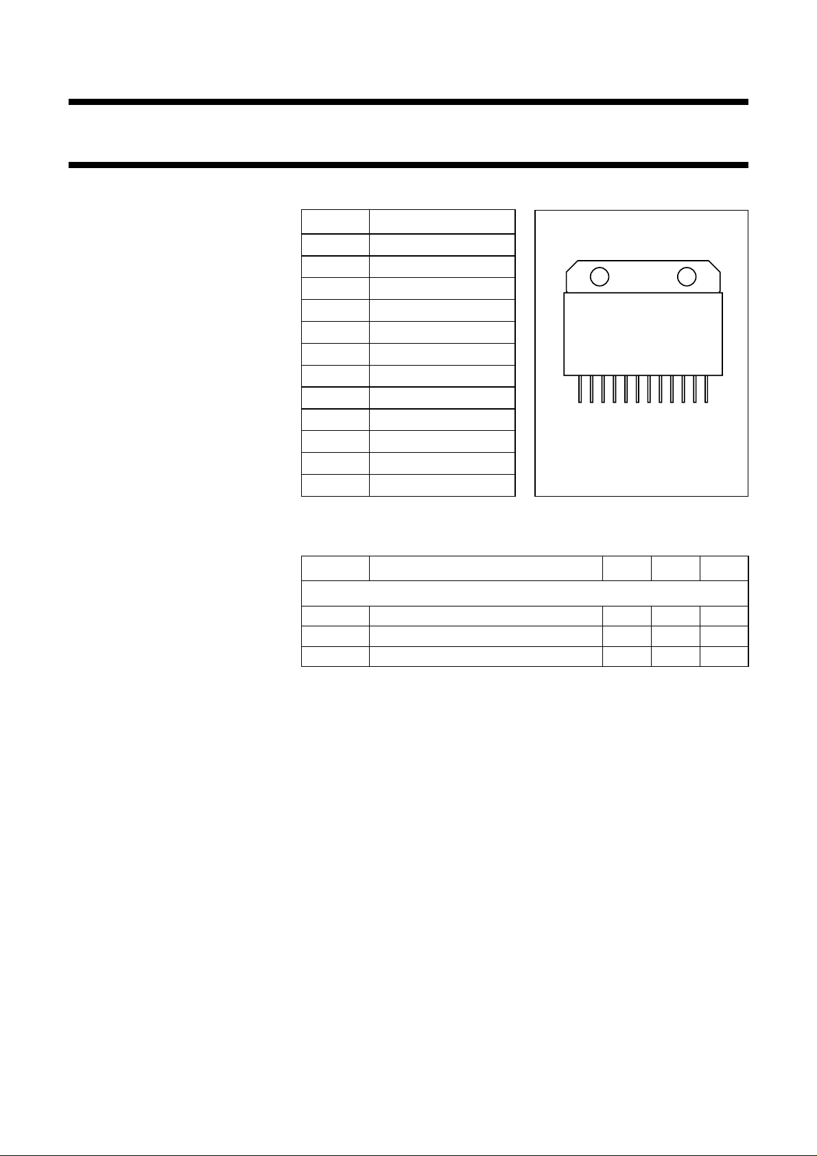
PINNING - SOT347
PIN DESCRIPTION
S1
S2
S3
)
1/3 page (Datasheet)
)
112
)
Front view
MBB934
Fig.1 Simplified outline.
10
11
12
1
2
3
4
5
6
7
8
9
supply voltage 1 (V
input 1
ground
output 1
supply voltage 2 (V
input 2
ground
output 2
supply voltage 3 (V
input 3
ground
output 3
LIMITING VALUES
In accordance with the Absolute Maximum Rating System (IEC 134).
SYMBOL PARAMETER MIN. MAX. UNIT
Per amplifier
V
S
T
mb
T
stg
supply voltage (DC) 80 90 V
operating mounting base temperature −20 +100 °C
storage temperature −40 +125 °C
1998 Feb 12 2
Page 3
Philips Semiconductors Product specification
Triple video driver hybrid amplifier CR6927
CHARACTERISTICS
V
= 85 V; TC=25°C; CL= 10 pF; output swing = 45 V (p-p) with 42.5 V DC offset (see Fig 7); unless otherwise
S
specified.
SYMBOL PARAMETER CONDITIONS MIN. TYP. MAX. UNIT
I
S
P
tot
t
r
t
f
BW small signal bandwidth between −3 dB points; note 2 140 150 − MHz
V
tilt
V
os
NLN non-linearity V
A
V
V
G
supply current open input and open output 85 100 115 mA
total power dissipation 25 MHz square wave − 10.6 12 W
rise time transient response 10 to 90%; note 1 − 2.5 3.1 ns
fall time transient response 10 to 90%; note 1 − 2.1 2.5 ns
low frequency tilt voltage 10 kHz square wave − 1.3 1.5 V
overshoot voltage (rise and
fall time)
adjustable by C1 and C2;
− 310%
see Fig 7
=5to75V − 25%
O
DC voltage gain 50 Ω source; note 3 11.2 12.4 13.6
insertion gain 50 Ω source; note 4 160 180 200
Notes
1. Input signal is a 100 kHz square wave of 3.8 V (p-p) with 1.5 V DC offset (50 Ω source).
2. Sinewave output signal: 1 V (p-p).
3. Measured V
at input test circuit.
O/VI
4. Measured VO/VI at input module.
60
V
MDA185
(V)
O
handbook, halfpage
2
V
I
(V)
1.8
1.6
1.4
1.2
1
02040 80
handbook, halfpage
5
V
I
(V)
3
1
−1
−3
020
40 80
60
MDA186
VO (V)
VS= 85V; TC=25°C; CL= 10pF; (R1 + R2) = 330 Ω;
output swing = 45 V (p-p) with 42 V DC offset.
Fig.2 Test circuit input voltage as a function of
output voltage; typical values.
1998 Feb 12 3
VS= 85 V; TC=25°C; CL= 10 pF; (R1 + R2) = 330 Ω;
output swing = 45 V (p-p) with 42 V DC offset.
Fig.3 Input voltage at input module as a
function of output voltage; typical values.
Page 4

Philips Semiconductors Product specification
Triple video driver hybrid amplifier CR6927
3.4
handbook, halfpage
t
r
(ns)
3.0
2.6
2.2
6
VS= 85 V; TC=25°C; CL= 10 pF; (R1 + R2) = 330 Ω;
output swing = 45 V (p-p) with 42 V DC offset.
10 14 18
Fig.4 Rise time as a function of load
capacitance; typical values.
MDA187
55 V (p-p)
45 V (p-p)
35 V (p-p)
CL (pF)
3.0
handbook, halfpage
t
f
(ns)
2.6
2.2
1.8
6
VS= 85 V; TC=25°C; CL= 10 pF; (R1 + R2) = 330 Ω;
output swing = 45 V (p-p) with 42 V DC offset.
10 14 18
Fig.5 Fall time as a function of load
capacitance; typical values.
MDA184
55 V (p-p)
45 V (p-p)
35 V (p-p)
CL (pF)
150 kΩ680 pF
4.3 kΩ
input
240 Ω 1.5 V
V
S
output
MDA188
Fig.6 Block diagram; single amplifier.
1998 Feb 12 4
Page 5

Philips Semiconductors Product specification
Triple video driver hybrid amplifier CR6927
V
handbook, full pagewidth
S
C3
TEST
FIXTURE
CR6927
POWER
SUPPLY
C2
R2
2
1
CR6927
FET
PROBE
4
3
output
C
L
SAMPLING
OSCILLOSCOPE
MBK283
C1
input
R1
R3
PULSE
GENERATOR
Speed-up circuit (R1, C1; R2, C2) ensures flat gain over the whole frequency range.
Fig.7 Application test circuit and block diagram.
Components used in test circuit (see Fig.7)
DESIGNATION DESCRIPTION VALUE
C1 variable capacitor 10 to 160 pF (typ. 68 pF)
C2 variable capacitor 10 to 160 pF (typ. 100 pF)
C3 chip capacitor plus electrolytic capacitor 10 nF plus 4.7 µF; 160 V
R1 resistor 270 Ω
R2 resistor 62 Ω
R3 resistor 50 Ω
Test equipment (see Fig.7)
EQUIPMENT TYPE DESCRIPTION
Pulse generator Le Croy; Model 9210 with unit 9212
Philips; Model PM5785B (125 MHz) with internal DC offset
Power supply Philips; Model PE1541, 80 V
FET probe Philips; Model PM8943, attenuation 100 : 1
Sampling oscilloscope Tektronix; Model 11803, sampling head SD24
1998 Feb 12 5
Page 6

Philips Semiconductors Product specification
Triple video driver hybrid amplifier CR6927
PACKAGE OUTLINE
Ceramic single-ended flat package; heatsink mounted; 2 mounting holes;
12 in-line tin (Sn) plated leads
D
y
U
q
P
A
F
SOT347
S
G
L
1
Z
DIMENSIONS (mm are the original dimensions)
A
UNIT
mm
6.0
5.6
cb
0.51
0.38
36.2
0.25 2.54
35.8
e
EUDG
18.2
17.8
e
2.0
b
0 5 10 mm
scale
L
P
min.
25.5
24.5
4.15
6
3.85
U
1
12
w
M
Q
qFSU
3.5
34.4
191.8
3.4
34.0
22.2
21.8
v
A
Q
A
v
0.250.3
w
0.1y4.1
1
E
c
Z
max.
OUTLINE
VERSION
SOT347
IEC JEDEC EIAJ
REFERENCES
1998 Feb 12 6
EUROPEAN
PROJECTION
ISSUE DATE
97-06-28
Page 7

Philips Semiconductors Product specification
Triple video driver hybrid amplifier CR6927
DEFINITIONS
Data sheet status
Objective specification This data sheet contains target or goal specifications for product development.
Preliminary specification This data sheet contains preliminary data; supplementary data may be published later.
Product specification This data sheet contains final product specifications.
Limiting values
Limiting values given are in accordance with the Absolute Maximum Rating System (IEC 134). Stress above one or
more of the limiting values may cause permanent damage to the device. These are stress ratings only and operation
of the device at these or at any other conditions above those given in the Characteristics sections of the specification
is not implied. Exposure to limiting values for extended periods may affect device reliability.
Application information
Where application information is given, it is advisory and does not form part of the specification.
LIFE SUPPORT APPLICATIONS
These products are not designed for use in life support appliances, devices, or systems where malfunction of these
products can reasonably be expected to result in personal injury. Philips customers using or selling these products for
use in such applications do so at their own risk and agree to fully indemnify Philips for any damages resulting from such
improper use or sale.
1998 Feb 12 7
Page 8

Philips Semiconductors – a worldwide company
Argentina: see South America
Australia: 34 Waterloo Road, NORTH RYDE, NSW 2113,
Tel. +61 2 9805 4455, Fax. +61 2 9805 4466
Austria: Computerstr. 6, A-1101 WIEN, P.O. Box 213, Tel. +43 160 1010,
Fax. +43 160 101 1210
Belarus: Hotel Minsk Business Center, Bld. 3, r. 1211, Volodarski Str. 6,
220050 MINSK, Tel. +375 172 200 733, Fax. +375 172 200 773
Belgium: see The Netherlands
Brazil: seeSouth America
Bulgaria: Philips Bulgaria Ltd., Energoproject, 15thfloor,
51 James Bourchier Blvd., 1407 SOFIA,
Tel. +359 2 689 211, Fax. +359 2 689 102
Canada: PHILIPS SEMICONDUCTORS/COMPONENTS,
Tel. +1 800 234 7381
China/Hong Kong: 501 Hong Kong Industrial Technology Centre,
72 Tat Chee Avenue, Kowloon Tong, HONG KONG,
Tel. +852 2319 7888, Fax. +852 2319 7700
Colombia: see South America
Czech Republic: see Austria
Denmark: Prags Boulevard 80, PB 1919, DK-2300 COPENHAGEN S,
Tel. +45 32 88 2636, Fax. +45 31 57 0044
Finland: Sinikalliontie 3, FIN-02630 ESPOO,
Tel. +358 9 615800, Fax. +358 9 61580920
France: 51 Rue Carnot, BP317, 92156 SURESNES Cedex,
Tel. +33 1 40 99 6161, Fax. +33 1 40 99 6427
Germany: Hammerbrookstraße 69, D-20097 HAMBURG,
Tel. +49 40 23 53 60, Fax. +49 40 23 536 300
Greece: No. 15, 25th March Street, GR 17778 TAVROS/ATHENS,
Tel. +30 1 4894 339/239, Fax. +30 1 4814 240
Hungary: seeAustria
India: Philips INDIA Ltd, Band Box Building, 2nd floor,
254-D, Dr. Annie Besant Road, Worli, MUMBAI 400 025,
Tel. +91 22 493 8541, Fax. +91 22 493 0966
Indonesia: see Singapore
Ireland: Newstead, Clonskeagh, DUBLIN 14,
Tel. +353 1 7640 000, Fax. +353 1 7640 200
Israel: RAPAC Electronics, 7 Kehilat Saloniki St, PO Box 18053,
TEL AVIV 61180, Tel. +972 3 645 0444, Fax. +972 3 649 1007
Italy: PHILIPS SEMICONDUCTORS, Piazza IV Novembre 3,
20124 MILANO, Tel. +39 2 6752 2531, Fax. +39 2 6752 2557
Japan: Philips Bldg 13-37, Kohnan 2-chome, Minato-ku, TOKYO 108,
Tel. +81 3 3740 5130, Fax. +81 3 3740 5077
Korea: Philips House, 260-199 Itaewon-dong, Yongsan-ku, SEOUL,
Tel. +82 2 709 1412, Fax. +82 2 709 1415
Malaysia: No. 76 Jalan Universiti, 46200 PETALING JAYA, SELANGOR,
Tel. +60 3 750 5214, Fax. +60 3 757 4880
Mexico: 5900 Gateway East, Suite 200, EL PASO, TEXAS 79905,
Tel. +9-5 800 234 7381
Middle East: see Italy
Netherlands: Postbus 90050, 5600 PB EINDHOVEN, Bldg. VB,
Tel. +31 40 27 82785, Fax. +31 40 27 88399
New Zealand: 2 Wagener Place, C.P.O. Box 1041, AUCKLAND,
Tel. +64 9 849 4160, Fax. +64 9 849 7811
Norway: Box 1, Manglerud 0612, OSLO,
Tel. +47 22 74 8000, Fax. +47 22 74 8341
Philippines: Philips Semiconductors Philippines Inc.,
106 Valero St. Salcedo Village, P.O. Box 2108 MCC, MAKATI,
Metro MANILA, Tel. +63 2 816 6380, Fax. +63 2 817 3474
Poland: Ul. Lukiska 10, PL 04-123 WARSZAWA,
Tel. +48 22 612 2831, Fax. +48 22 612 2327
Portugal: see Spain
Romania: see Italy
Russia: Philips Russia, Ul. Usatcheva 35A, 119048 MOSCOW,
Tel. +7 095 755 6918, Fax. +7 095 755 6919
Singapore: Lorong 1, Toa Payoh, SINGAPORE 1231,
Tel. +65 350 2538, Fax. +65 251 6500
Slovakia: see Austria
Slovenia: see Italy
South Africa: S.A. PHILIPS Pty Ltd., 195-215 Main Road Martindale,
2092 JOHANNESBURG, P.O. Box 7430 Johannesburg 2000,
Tel. +27 11 470 5911, Fax. +27 11 470 5494
South America: Al. Vicente Pinzon, 173, 6th floor,
04547-130 SÃO PAULO, SP, Brazil,
Tel. +55 11 821 2333, Fax. +55 11 821 2382
Spain: Balmes 22, 08007 BARCELONA,
Tel. +34 3 301 6312, Fax. +34 3 301 4107
Sweden: Kottbygatan 7, Akalla, S-16485 STOCKHOLM,
Tel. +46 8 632 2000, Fax. +46 8 632 2745
Switzerland: Allmendstrasse 140, CH-8027 ZÜRICH,
Tel. +41 1 488 2686, Fax. +41 1 488 3263
Taiwan: Philips Semiconductors, 6F, No. 96, Chien Kuo N. Rd., Sec. 1,
TAIPEI, Taiwan Tel. +886 2 2134 2865, Fax. +886 2 2134 2874
Thailand: PHILIPS ELECTRONICS (THAILAND) Ltd.,
209/2 Sanpavuth-Bangna Road Prakanong, BANGKOK 10260,
Tel. +66 2 745 4090, Fax. +66 2 398 0793
Turkey: Talatpasa Cad. No. 5, 80640 GÜLTEPE/ISTANBUL,
Tel. +90 212 279 2770, Fax. +90 212 282 6707
Ukraine: PHILIPS UKRAINE, 4 Patrice Lumumba str., Building B, Floor 7,
252042 KIEV, Tel. +380 44 264 2776, Fax. +380 44 268 0461
United Kingdom: Philips Semiconductors Ltd., 276 Bath Road, Hayes,
MIDDLESEX UB3 5BX, Tel. +44 181 730 5000, Fax. +44 181 754 8421
United States: 811 East Arques Avenue, SUNNYVALE, CA 94088-3409,
Tel. +1 800 234 7381
Uruguay: see South America
Vietnam: see Singapore
Yugoslavia: PHILIPS, Trg N. Pasica 5/v, 11000 BEOGRAD,
Tel. +381 11 625 344, Fax.+381 11 635 777
For all other countries apply to: Philips Semiconductors,
International Marketing & Sales Communications, Building BE-p, P.O. Box 218,
5600 MD EINDHOVEN, The Netherlands, Fax. +31 40 27 24825
© Philips Electronics N.V. 1998 SCA57
All rights are reserved. Reproduction in whole or in part is prohibited without the prior written consent of the copyright owner.
The information presented in this document does not form part of any quotation or contract, is believed to be accurate and reliable and may be changed
without notice. No liability will be accepted by the publisher for any consequence of its use. Publication thereof does not convey nor imply any license
under patent- or other industrial or intellectual property rights.
Internet: http://www.semiconductors.philips.com
Printed in The Netherlands 125102/00/03/pp8 Date of release: 1998 Feb 12 Document order number: 9397 750 03306
 Loading...