

Philips CR6729A Datasheet

DISCRETE SEMICONDUCTORS
DATA SH EET
ook, halfpage
M3D299
CR6729A
Triple video driver hybrid amplifier
Product specification
Supersedes data of 1998 Aug 06
1998 Sep 21
Philips Semiconductors Product specification
Triple video driver hybrid amplifier CR6729A
FEATURES
• Transition times (10 to 90%) with 45 V (p-p) swing and
CL= 10 pF:
– rise time (typ.) 2.5 ns
– fall time (typ.) 2.1 ns
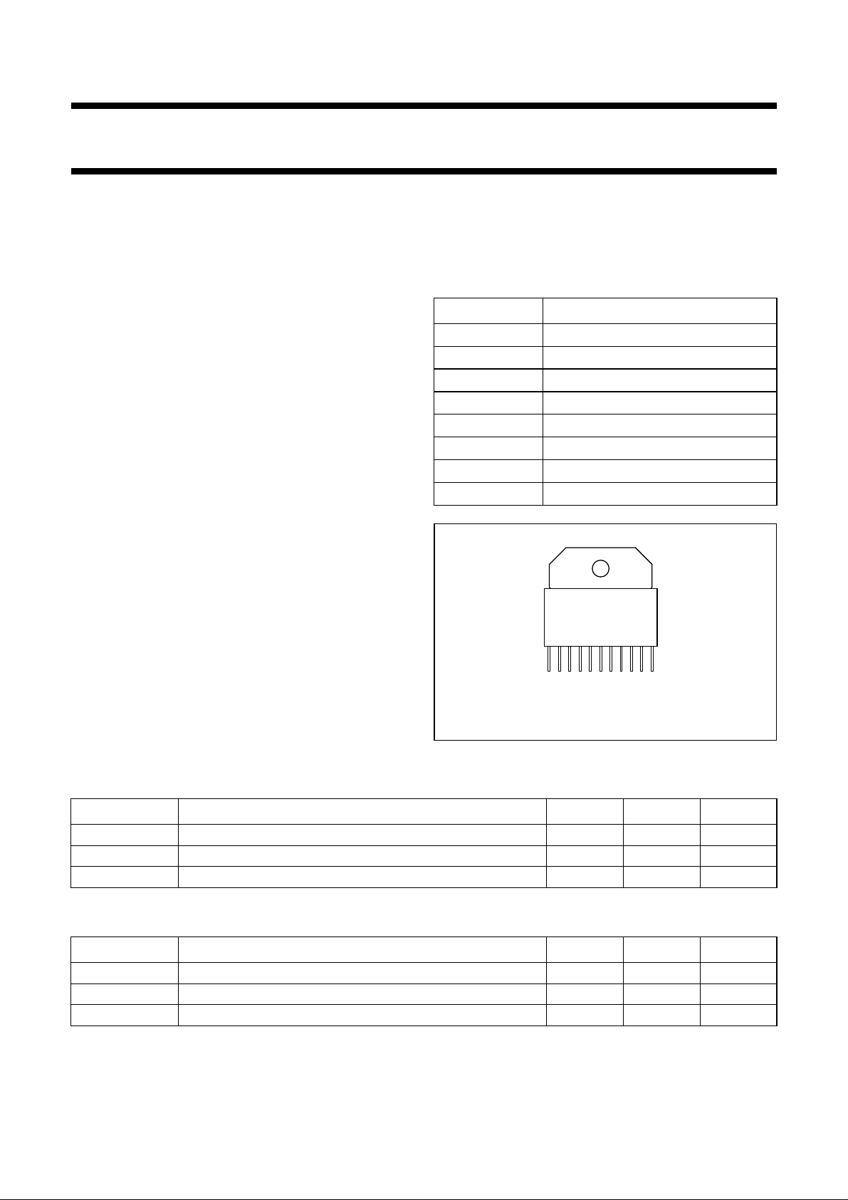
• Small 11-pin package
• Optimized for low supply voltages up to 70 V
• Design optimized for excellent smearing performance
• Low power consumption: 10 W with 25 MHz square
wave
• Gold metallization ensures excellent reliability.
DESCRIPTION
The CR6729A is a 3-channel hybrid RGB-amplifier module
in an 11-pin SOT451A package. Being an Active Load
amplifier, the CR6729A combines a high bandwidth with a
relatively low and constant dissipation. It is the
pin-compatible 11-pin successor to the 12-pin CR6728A
and CR6727A modules.
An optimized design, together with innovative application
recommendations, ensure excellent smearing
performance.
APPLICATIONS
• High-end CRT monitors with supply voltages up to 70 V
and pixel frequencies up to 250 MHz.
PINNING
PIN DESCRIPTION
1
2, 6, 10
3
4, 8
5
7
9
11
handbook, halfpage
input 1
ground
output 1
supply voltage (V
input 2
output 2
input 3
output 3
)
S
A member of the ‘29-family’ of active loads, the CR6729A
is intended for relatively low supply voltages up to 70 V.
Other ‘29-family’ members are intended for supply
111
Front view
MBK056
voltages up to 90 V, and low static dissipation (CR6929) or
highest monitor performance (CR6929A).
Fig.1 Simplified outline SOT451A.
LIMITING VALUES
In accordance with the Absolute Maximum Rating System (IEC 134).
SYMBOL PARAMETER MIN. MAX. UNIT
V
S
T
mb
T
stg
supply voltage (DC) − 85 V
operating mounting base temperature −20 +110 °C
storage temperature −40 +125 °C
RECOMMENDED OPERATING CONDITIONS
SYMBOL PARAMETER MIN. MAX. UNIT
V
S
T
mb
T
stg
supply voltage (DC) − 70 V
operating mounting base temperature −20 +100 °C
storage temperature −40 +125 °C
1998 Sep 21 2
Philips Semiconductors Product specification
Triple video driver hybrid amplifier CR6729A
CHARACTERISTICS
VS= 65 V; Tmb=25°C; CL= 10 pF; output swing = 45 V (p-p) with 32 V DC offset (see Fig.3); unless otherwise
specified.
SYMBOL PARAMETER CONDITIONS MIN. TYP. MAX. UNIT
Per amplifier
I
S
P
tot
t
r
t
f
BW small signal bandwidth between −3 dB points; note 2 140 150 − MHz
V
tilt
V
os
NLN non-linearity V
A
V
V
G
supply current open input and open output 93 108 123 mA
total power dissipation 25 MHz square wave − 10 11.5 W
rise time transient response 10 to 90%; note 1 − 2.5 3.1 ns
fall time transient response 10 to 90%; note 1 − 2.1 2.5 ns
low frequency tilt voltage 10 kHz square wave − 1.3 1.5 V
overshoot voltage (rise and
fall time)
adjustable by C1 and C2;
− 310%
see Fig.3
=15to55V − 25%
O
DC voltage gain 50 Ω source; note 3 10.8 12.0 13.6 V/V
insertion gain 50 Ω source; note 4 194 214 234 V/V
Notes
1. Input signal is a 100 kHz square wave of 3.4 V (p-p) with 1 V DC offset (50 Ω source), without R
2. Sinewave output signal: 1 V (p-p).
3. Measured VO/VI at input test circuit.
4. Measured VO/VI at input module.
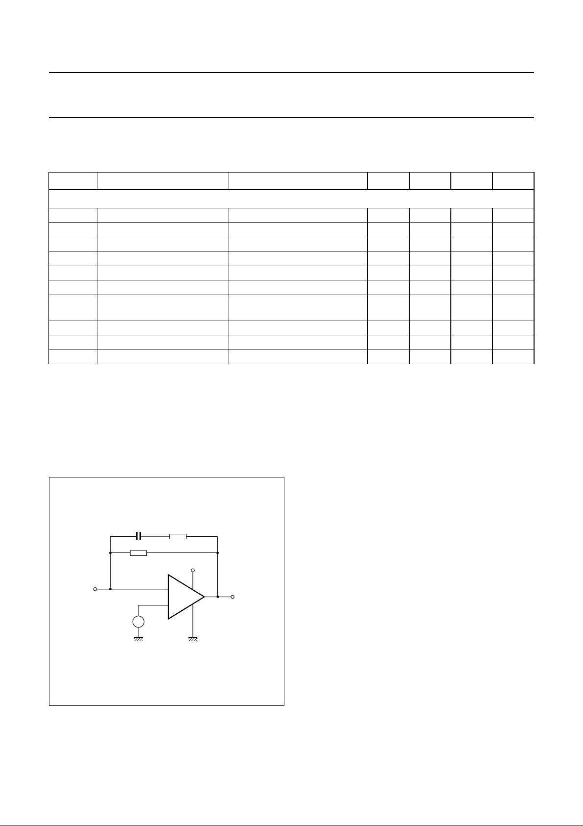
APPLICATION NOTES
1.5 V
150 kΩ680 pF
V
S
output
MDA861
handbook, halfpage
4.3 kΩ
input
level
.
Fig.2 Block diagram, single amplifier.
1998 Sep 21 3
 Loading...