

Philips cr6727a DATASHEETS
DISCRETE SEMICONDUCTORS
DATA SH EET
ook, halfpage
M3D156
CR6727A
Triple video driver hybrid amplifier
Product specification
Supersedes data of 1997 Oct 02
1998 Feb 12
File under Discrete Semiconductors, SC05
Philips Semiconductors Product specification
Triple video driver hybrid amplifier CR6727A
FEATURES
• Transition times (10 to 90%)
with 45 V (p-p) swing
and CL= 10 pF:
rise time (typ.) 2.5 ns
fall time (typ.) 2.1 ns
• Low power consumption:
10 W with 25 MHz square wave
• Minimum small signal bandwidth:
140 MHz at 1 V (p-p) or
120 MHz at 40 V (p-p)
• Very fast slew rate: 16000 V/µs
• Internal smearing compensation
• Excellent grey-scale linearity
• Unconditional stability
• Gold metallization ensures
excellent reliability.
APPLICATIONS
• Cathode-ray tube (CRT) drivers in
high-resolution colour monitors.
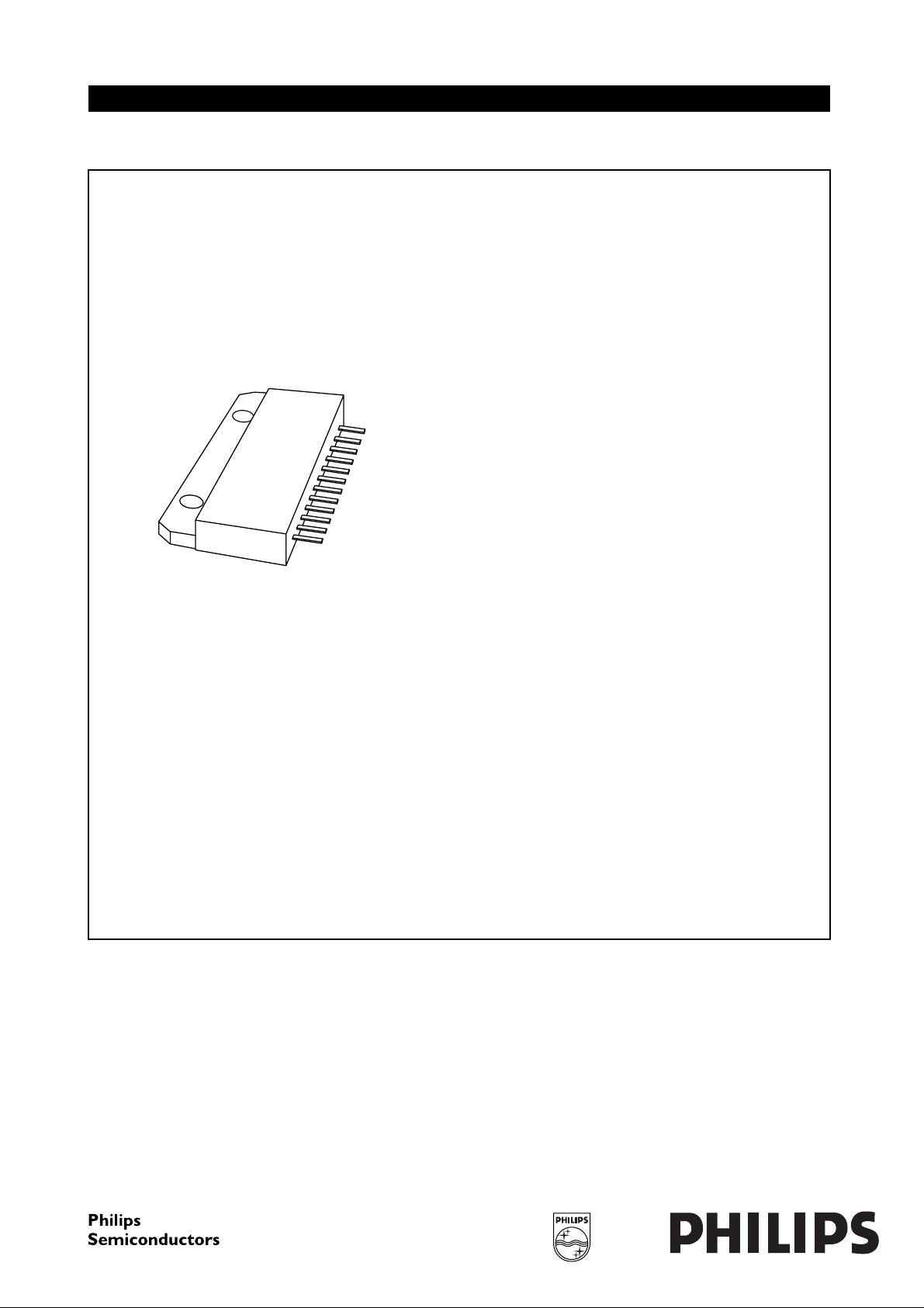
DESCRIPTION
Hybrid amplifier module comprising
three video amplifiers in a SOT347
package.
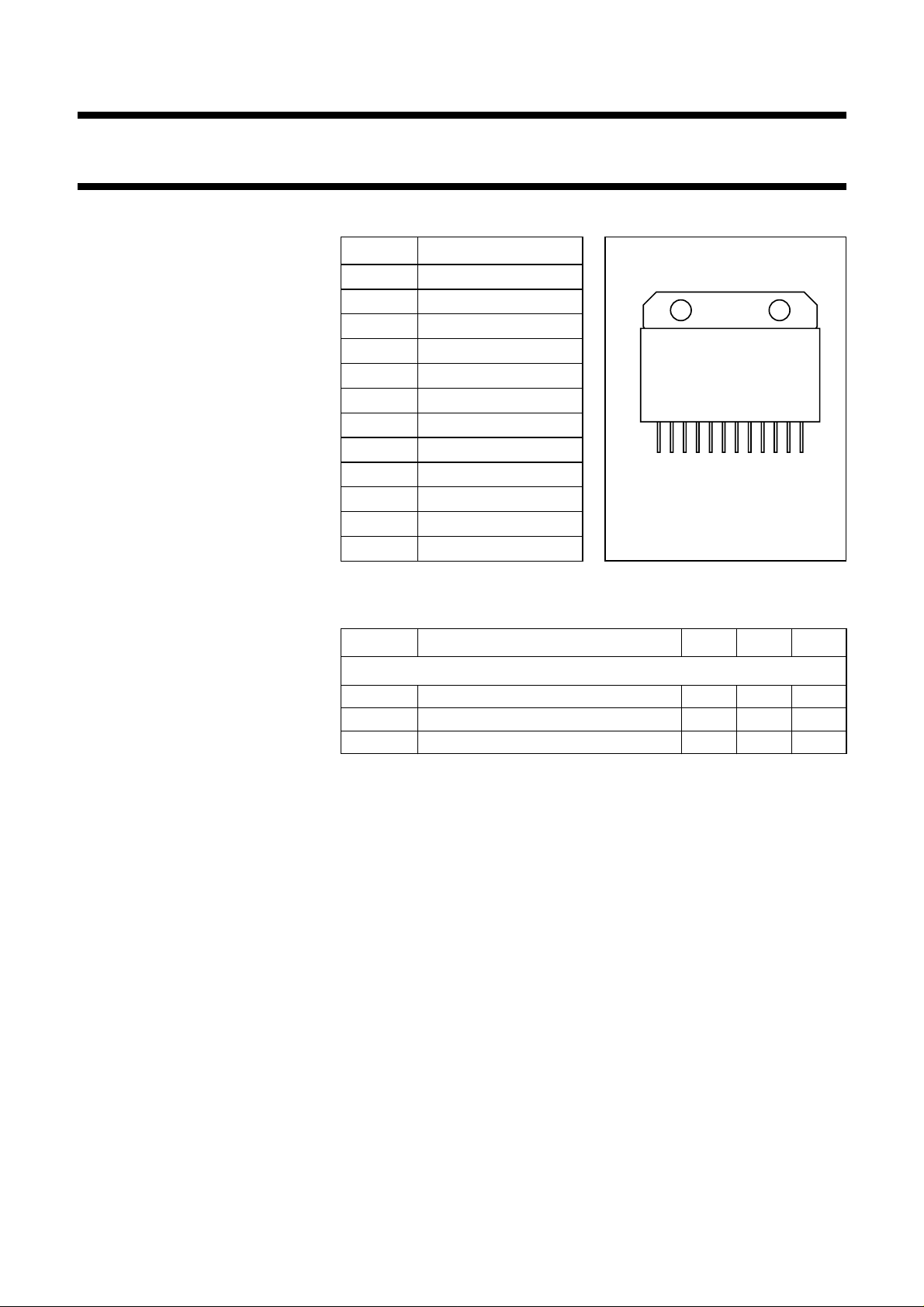
PINNING - SOT347
PIN DESCRIPTION
S1
S2
S3
)
1/3 page (Datasheet)
)
112
)
Front view
MBB934
Fig.1 Simplified outline.
10
11
12
1
2
3
4
5
6
7
8
9
supply voltage 1 (V
input 1
ground
output 1
supply voltage 2 (V
input 2
ground
output 2
supply voltage 3 (V
input 3
ground
output 3
LIMITING VALUES
In accordance with the Absolute Maximum Rating System (IEC 134).
SYMBOL PARAMETER MIN. MAX. UNIT
Per amplifier
V
S
T
mb
T
stg
supply voltage (DC) 60 70 V
operating mounting base temperature −20 +100 °C
storage temperature −40 +125 °C
1998 Feb 12 2
Philips Semiconductors Product specification
Triple video driver hybrid amplifier CR6727A
CHARACTERISTICS
VS= 65 V; TC=25°C; CL= 10 pF; output swing = 45 V (p-p) with 32 V DC offset (see Fig.3); unless otherwise
specified.
SYMBOL PARAMETER CONDITIONS MIN. TYP. MAX. UNIT
I
S
P
tot
t
r
t
f
BW small signal bandwidth between −3 dB points; note 2 140 150 − MHz
V
tilt
V
os
NLN non-linearity V
A
V
V
G
supply current open input and open output 105 120 135 mA
total power dissipation 25 MHz square wave − 11 11.5 W
rise time transient response 10 to 90%; note 1 − 2.5 3.1 ns
fall time transient response 10 to 90%; note 1 − 2.1 2.5 ns
low frequency tilt voltage 10 kHz square wave − 1.3 1.5 V
overshoot voltage (rise and
fall time)
adjustable by C1 and C2;
− 310%
see Fig.3
=5to55V − 25%
O
DC voltage gain 50 Ω source; note 3 11.2 12.4 13.6
insertion gain 50 Ω source; note 4 160 180 200
Notes
1. Input signal is a 100 kHz square wave of 3.8 V (p-p) with 1.5 V DC offset (50 Ω source).
2. Sinewave output signal: 1 V (p-p).
3. Measured V
at input test circuit.
O/VI
4. Measured VO/VI at input module.
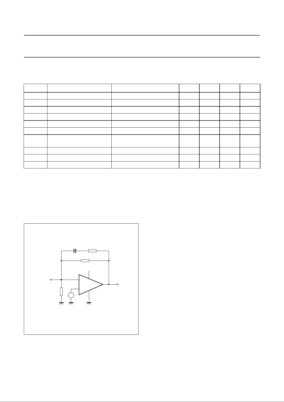
APPLICATION NOTES
handbook, halfpage
input
680 pF
240 Ω
1.5 V
4.3 kΩ
150 kΩ
V
S
output
MGK638
Fig.2 Block diagram; single amplifier.
1998 Feb 12 3
 Loading...