

Philips CR5527S Datasheet

DISCRETE SEMICONDUCTORS
DATA SH EET
CR5527S
Triple video driver hybrid amplifier
Product specification
Supersedes data of June 1993
File under Discrete Semiconductors, SC05
Philips Semiconductors
1995 Apr 05
Philips Semiconductors Product specification
Triple video driver hybrid amplifier CR5527S
FEATURES
• Typical transition times (10 to 90%)
with CL=10pF:
– at 50 V (p-p) swing
tr= 3 ns; tf= 2.2 ns
• Low power consumption
• Minimum small signal
bandwidth 100 MHz
• Very fast slew rate; 12000 V/µs
• Excellent grey-scale linearity
• Unconditional stability
• Gold metallization ensures
excellent reliability.
APPLICATIONS
It is designed for application in
cathode-ray tube (CRT) drivers in
high-resolution colour monitors.
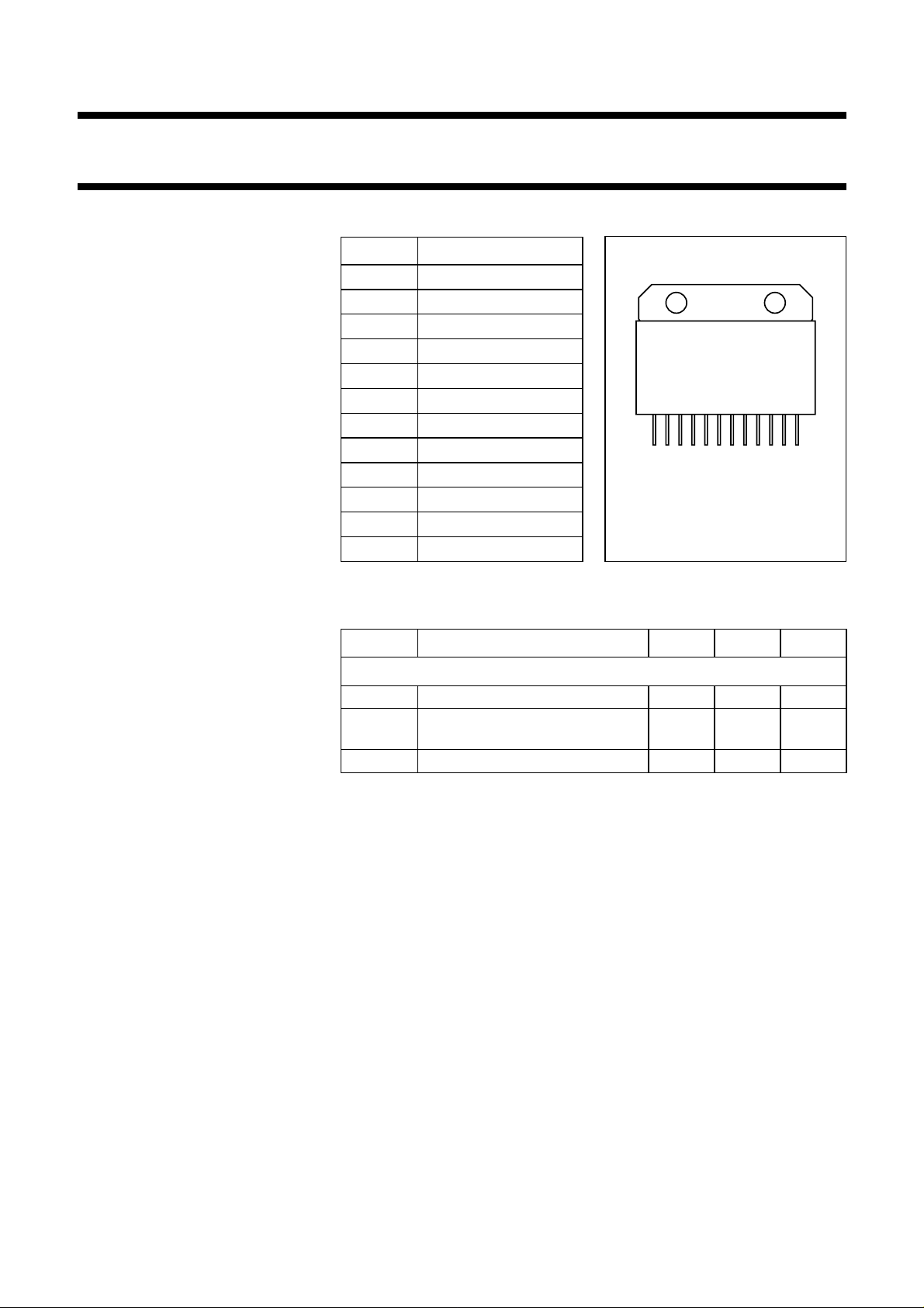
DESCRIPTION
PINNING
PIN DESCRIPTION
S1
S2
S3
)
1/3 page (Datasheet)
)
)
112
Front view
MBB934
Fig.1 SOT347.
10
11
12
1
2
3
4
5
6
7
8
9
supply voltage 1 (V
input 1
ground
output 1
supply voltage 2 (V
input 2
ground
output 2
supply voltage 3 (V
input 3
ground
output 3
LIMITING VALUES
In accordance with the Absolute Maximum Rating System (IEC 134).
SYMBOL PARAMETER MIN. MAX. UNIT
Hybrid amplifier module comprising
three video amplifiers in a SOT347
package.
Per amplifier
V
S
T
mb
supply voltage (DC) − 90 V
operating mounting base
−20 +100 °C
temperature; note 1
T
stg
storage temperature −40 +125 °C
Note
1. To ensure proper thermal contact, a layer of heatsink compound should be
applied between module and heatsink.
1995 Apr 05 2

Philips Semiconductors Product specification
Triple video driver hybrid amplifier CR5527S
CHARACTERISTICS
VS= 80 V; Tmb=25°C; CL= 10 pF; R1 = 348 Ω; C1 = 90 pF; R2 = 82 Ω; C2 = 100 pF; 50 V (p-p) output swing
with 40 V DC offset (see Fig.6); unless otherwise specified.
SYMBOL PARAMETER CONDITIONS MIN. TYP. MAX. UNIT
Per amplifier
I
S
P
tot
t
r
t
f
BW small signal bandwidth between −3 dB points; note 2 100 110 − MHz
V
tilt
V
os
NLN non-linearity V
A
V
V
G
supply current input and output open 19 25 31 mA
total power dissipation 25 MHz square wave − 9.6 11 W
rise time transient response 10 to 90%; note 1 − 34ns
fall time transient response 10 to 90%; note 1 − 2.2 3 ns
low frequency tilt voltage 10 kHz square wave − 1.3 1.5 V
overshoot voltage varied by C1 and C2; see Fig.6 − 310%
=5to75V − 25%
O
DC voltage gain 50 Ω source; note 3 11 12 13
insertion gain 50 Ω source; note 4 350 370 390
Notes
1. Input signal is a 100 kHz square wave of 4.15 V (p-p), with 1.5 V DC offset (50 Ω source).
2. Sinewave output signal: 1 V (p-p).
3. Measured V
(Fig.2) at input test-circuit (see Fig.6).
O/VI
4. Measured VO/VI (Fig.3) at input module (see Fig.6).
1995 Apr 05 3
Philips Semiconductors Product specification
Triple video driver hybrid amplifier CR5527S
handbook, halfpage
6
V
I
(V)
4
2
0
2
0 20406080
VS= 80V; Tmb=25°C; CL= 10pF; R1 = 348 Ω; C1 = 90 pF;
R2 = 82 Ω; C2 = 100 pF; 50 V (p-p) output swing with 40 V DC offset.
MLB220
V
(V)
O
Fig.2 Input voltage at input test-circuit as a
function of output voltage; typical values.
2.0
handbook, halfpage
V
I
(V)
1.8
1.6
1.4
1.2
1
020406080
VS= 80 V; Tmb=25°C; CL= 10 pF; R1 = 348 Ω; C1 = 90 pF;
R2 = 82 Ω; C2 = 100 pF; 50 V (p-p) output swing with 40 V DC offset.
MLB219
V
(V)
O
Fig.3 Input voltage at input module as a function
of output voltage; typical values.
4.25
handbook, halfpage
t
r
(ns)
3.75
3.25
2.75
10 14 18 22
VS= 80 V; Tmb=25°C; CL= 10 pF; R1 = 348 Ω; C1 = 90 pF;
R2 = 82 Ω; C2 = 100 pF; 55, 50, 40 V (p-p) output swing
with 40 V DC offset.
MLC952
55 V (p-p)
50 V (p-p)
40 V (p-p)
(pF)C
L
Fig.4 Rise time transient response as a function
of load capacitance; typical values.
3.5
handbook, halfpage
t
f
(ns)
3.0
2.5
2.0
10 14 18 22
VS= 80 V; Tmb=25°C; CL= 10 pF; R1 = 348 Ω; C1 = 90 pF;
R2 = 82 Ω; C2 = 100 pF; 55, 50, 40 V (p-p) output swing
with 40 V DC offset.
55 V (p-p)
50 V (p-p)
40 V (p-p)
CL(pF)
Fig.5 Fall time transient response as a function
of load capacitance; typical values.
MLC953
1995 Apr 05 4
 Loading...