

Philips CR5427 Datasheet
ook, halfpage
DISCRETE SEMICONDUCTORS
M3D299
CR5427
Triple video driver hybrid amplifier
Product specification
File under Discrete Semiconductors, SC05
1997 Oct 21
Philips Semiconductors Product specification
Triple video driver hybrid amplifier CR5427
FEATURES
• Transition times (10 to 90%)
with 45 V (p-p) swing
and CL= 10 pF:
rise time (typ.) 3 ns
fall time (typ.) 3 ns
• Very low power consumption:
7 Watt with 25 MHz square wave
• Minimum small signal bandwidth:
100 MHz
• Very fast slew rate 12000 V/µs
• Excellent grey-scale linearity
• Internal supply decoupling per
channel for optimum EMI
performance and minimal crosstalk
• Gold metallization ensures
excellent reliability
• No negative supply required in the
final stage.
APPLICATIONS
• Cathode-ray tube (CRT) drivers in
high-resolution colour monitors
• For 1280 x 1024 pixels (good
picture quality) with single PNP
buffer
• For 1024 x 768 pixels (acceptable
picture quality) when directly driven
from the video pre-amp IC.
DESCRIPTION
Hybrid amplifier module comprising
three video amplifiers in a SOT451A
package.
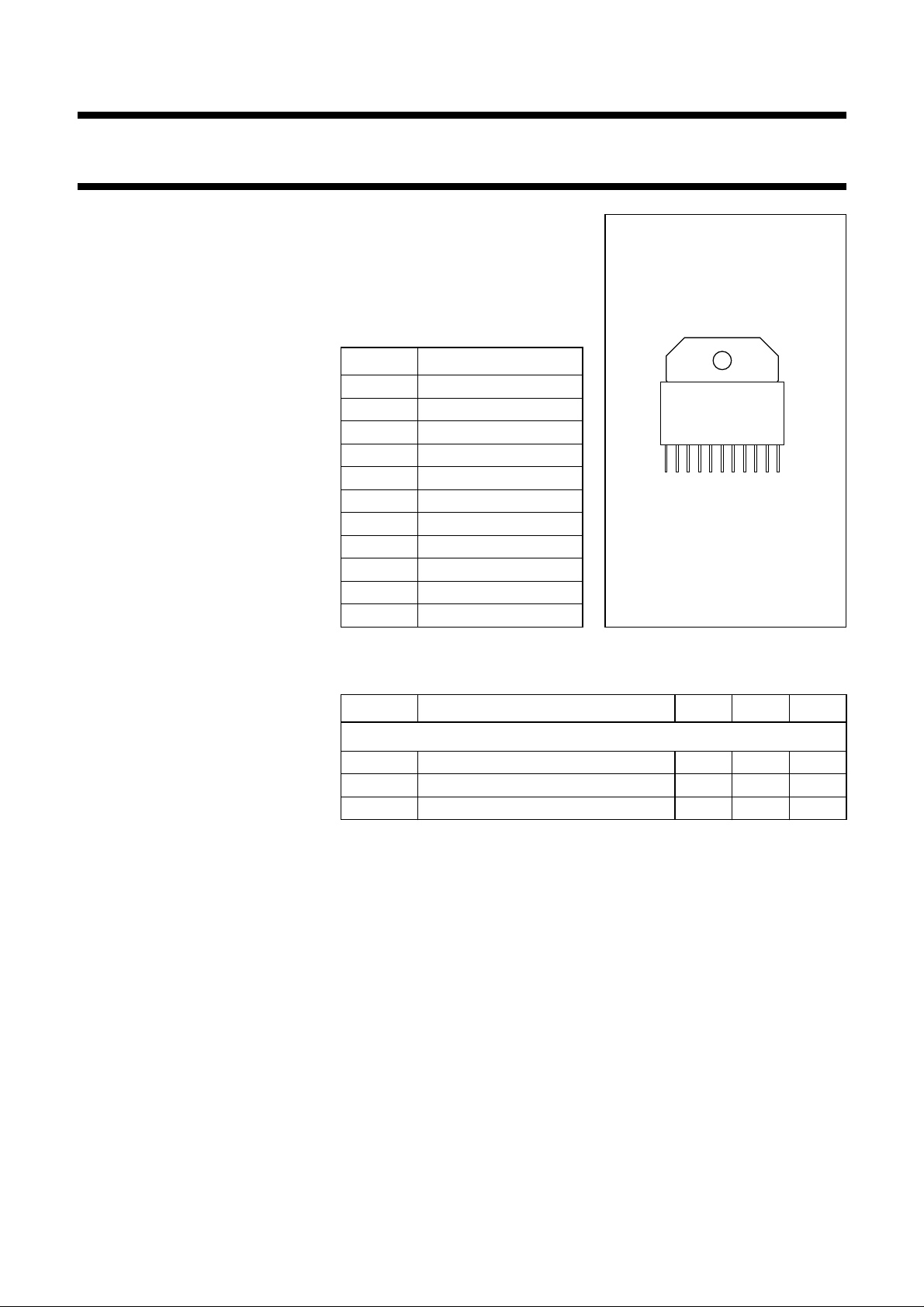
PINNING - SOT451A
page
PIN DESCRIPTION
1 input 1
2 ground
3 output 1
4 supply voltage (V
5 input 2
)
S
111
Front view
MBK056
6 ground
7 output 2
8 supply voltage (V
)
S
9 input 3
10 ground
Fig.1 Simplified outline.
11 output 3
LIMITING VALUES
In accordance with the Absolute Maximum Rating System (IEC 134).
SYMBOL PARAMETER MIN. MAX. UNIT
Per amplifier
V
T
mb
T
stg
supply voltage (DC) − 80 V
S
operating mounting base temperature −20 +100 °C
storage temperature −40 +125 °C
1997 Oct 21 2
Philips Semiconductors Product specification
Triple video driver hybrid amplifier CR5427
CHARACTERISTICS
V
= 75 V; TC=25°C; CL= 10 pF; output swing = 45 V (p-p) with 32.5 V DC offset (see Fig.3); unless otherwise
S
specified.
SYMBOL PARAMETER CONDITIONS MIN. TYP. MAX. UNIT
I
S
P
tot
t
r
t
f
BW small signal bandwidth between −3 dB points; note 2 100 120 − MHz
V
tilt
V
os
NLN non-linearity V
A
V
V
G
supply current open input and open output 50 60 75 mA
total power consumption 25 MHz square wave − 78W
rise time transient response 10 to 90%; note 1 − 34ns
fall time transient response 10 to 90%; note 1 − 34ns
low frequency tilt voltage 10 kHz square wave − 1.3 1.5 V
overshoot voltage (rise and
fall time)
adjustable by C1 and C2;
− 310%
see Fig.3
=10to60V − 25%
O
DC voltage gain 50 Ω source; note 3 11 12.5 14
insertion gain 50 Ω source; note 4 110 130 150
Notes
1. Input signal is a 100 kHz square wave of 3.5 V (p-p) with 3.5 V DC offset (50 Ω source).
2. Sinewave output signal: 1 V (p-p).
3. Measured V
at input test circuit.
O/Vi
4. Measured VO/Vi at input module.
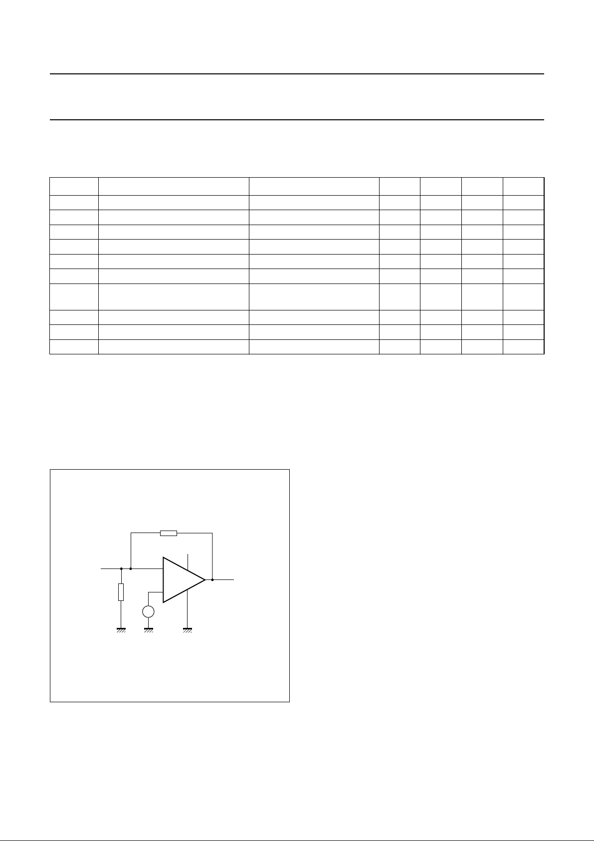
APPLICATION NOTES
handbook, halfpage
input
1.5
kΩ
10 kΩ
4 V
V
S
−
output
+
MGK730
Fig.2 Block diagram; single amplifier.
1997 Oct 21 3
 Loading...