

Page 1
15" TFT LCD Colour Monitor
Horizontal frequencies
47 - 63 kHz
Service
Service
Service
TABLE OF CONTENTS
SAFETY NOTICE
Published by BCU Monitor Printed in Taiwan Copyright reserved Subject to modification Sep. 10 2003
GB
3138 106 10308
Compaq fp5315
AJ2S4M/02
w/ audio
XH3 HP 15”
Important Safety Notice .................................. 2
Technical Data & Power Management.............. 3
Factory Mode .......................................... ...... 8
............................................10
Definition of Pixel Defects.............................. 13
Mechanical Instructions .................................14~15
Connecting to PC & the Monitor Front panel......4
OSD manu ..................................................... 5
Warning Message......... ..................................6
OSD Aging Mode & Lock/unlock.......................7
Failure mode of LCD panel...............................9
Troubleshooting
Wiring Diagram..............................................11
Flat Panel Adjust ...........................................12
Safety Test Requirements ..............................16
Electrical Instructions............................. .......17
Display Adjustment........................................18~19
DDC Instructions and DDC Data .................... 20~25
ISP Instruction...............................................26
Repair Flow Chart...........................................27~29
Repair tips .....................................................30
~32
D-SUB / DVI Diagram .....................................33
ROM Diagram ................................................34
Scaler Diagram ..............................................35~36
Control board Diagram and (C.B.A) ................ 39
Power board Diagram .................................... 40~41
Scaler board C.B.A-1&-2.................................44
Spare Parts List
Function Block Diagram..................................31
Power Diagram ..............................................37
Audio Diagram............................................... 38
Power board C.B.A.-1&-2................................42~43
Exploded View................................................45
Recommended Parts List & ....46~47
General product Specification ........................ 48~63
Different Parts List..........................................64~65
Description
Description
Page
Page
REFER TO BACK COVER FOR IMPORTANT SAFETY GUIDELINES
CAUTION: USE A SEPARATE ISOLATION TRANSFORMER FOR THIS UNIT WHEN SERVICING.
ANY PERSON ATTEMPTING TO SERVICE THIS CHASSIS MUST FAMILIARIZE HIMSELF WITH THE CHASSIS
AND BE AWARE OF THE NECESSARY SAFETY PRECAUTIONS TO BE USED WHEN SERVICING ELECTRONIC
EQUIPMENT CONTAINING HIGH VOLTAGES.
S
HP L1523
AJ6S4M/02
w/ audio
HP L1502
AJ6S40/02
w/o audio
Page 2

IMPORTANT SAFETY NOTICE
2
9
Go to cover page
HP L1502
FOR PRODUCTS CONTAINING LASER :
DANGER- Invisible laser radiation when open.
AVOID DIRECT EXPOSURE TO BEAM.
CAUTION- Use of controls or adjustments or
performance of procedures other than
those specified herein may result in
hazardous radiation exposure.
CAUTION- The use of optical instruments with this
product will increase eye hazard.
TO ENSURE THE CONTINUED RELIABILITY OF THIS
PRODUCT, USE ONLY ORIGINAL MANUFACTURER'S
REPLACEMENT PARTS, WHICH ARE LISTED WITH THEIR
PART NUMBERS IN THE PARTS LIST SECTION OFTHIS
SERVICE MANUAL.
Proper service and repair is important to the safe, reliable
operation of all HPConsumer Electronics Company**
Equipment. The service procedures recommended by HP and
described in this service manual are effective methods of
performing service operations. Some ofthese service
operations require the use of tools specially designed for the
purpose. The special tools should be used when and as
recommended.
It is important to note that this manual contains various
CAUTIONS and NOTICES which should be carefully read in
order to minimize the risk of personal injury to service
personnel. The possibility exists thatimproper service
methods may damage the equipment. It is also important to
understand that these CAUTIONS and NOTICES ARE NOT
EXHAUSTIVE. HP could not possibly know, evaluate and
advise the service trade ofall conceivable ways in which
service might be done or of the possible hazardous
consequences of each way. Consequently, HP has not
undertaken any such broad evaluation. Accordingly, a
servicer who uses aservice procedure or tool which is not
recommended by HP must first satisfy himself thoroughly that
neither his safety nor the safe operation of the equipment will
be jeopardized by the service method selected.
* * Hereafter throughout this manual, HP Consumer
Electronics Company will bereferred to as HP.
WARNING
Critical components having special safety characteristics are
identified with a bythe Ref. No. in the parts list and
enclosed within a broken line*
(where several critical components are grouped in one area)
along with the safety symbol on the schematicsor
exploded views.
Use of substitute replacement parts which do nothave the
same specified safety characteristics may create shock, fire,
or other hazards.
Under no circumstances should the original design be
modified or altered without written permission from Philips.
Philips assumes no liability, express or implied, arising out of
any unauthorized modification of design.
Servicer assumes all liability.
* Broken Line
Take care during handling the LCD module with backlight
unit
- Must mount the module using mounting holes arranged infour
corners.
- Do not press on the panel, edge of theframe strongly or electric
shock as this will result in damage to the screen.
- Do not scratch orpress on the panel with any sharp objects, such
as pencil or pen asthis may result in damage to the panel.
- Protect the module from the ESD as it may damage the electronic
circuit (C-MOS).
- Make certain that treatment person s body are grounded through
wrist band.
- Do not leave the module in high temperature and in areas of high
humidity for a long time.
- Avoid contact withwater as it may ashort circuit within the module.
- If the surface ofpanel become dirty, please wipe it off with a soft
material. (Cleaning with a dirty or rough cloth may damage the
panel.)
Page 3
HP L1502
PIN MNEMONIC SIGNAL
1 RV Red Video
2 GV Green Video/Sync on Green
3 BV Blue Video
4 NC None
5 GND Ground (DDC Return) or Cable detect
6RGRedGND
7 GG Green GND
8BGBlueGND
9+5V+5V
10 SG Sync GND or Cable detect
11 NC None
12 SDA DDC Data
13 HS Horizontal Sync
14 VS Vertical Sync
15 SCL DDC Clock
CPU
State
Monitor
State
Maximum
Power
(Watts)
Power
Switch LED
Color
Full Power Full Power 25 Green
Sleep Sleep 2 Amber
- Switch Off 2 (LED off)
FACTORY PRESET DISPLAY MODES
Preset
Pixel
Format
Horz
Freq
(KHz)
Horz
Polarit
y
Vert
Freq
(Hz)
Vert
Polarity
Pixel
Clk
(MHz) Source
1 640 x
480
31.469 - 59.940 - 25.175 VGA
2 640 x
480
37.861 - 72.809 - 31.500 VESA
3 640 x
480
37.500 - 75.000 - 31.500 VESA
4 720 x
400
31.469 - 70.087 + 28.322 VGA
5 800 x
600
37.879 + 60.317 + 40.000 VESA
6 800 x
600
48.077 + 72.188 + 50.000 VESA
7 800 x
600
46.875 + 75.000 + 49.500 VESA
8 832 x
624
49.726 +/- 74.551 +/- 57.284 MAC
9 1024 x
768
48.363 - 60.004 - 65.000 VESA
10 1024 x
768
56.476 - 70.069 - 75.000 VESA
11 1024 x
768
60.023 + 75.029 + 78.750 VESA
3
Technical Specifications
Technical Data
Go to cover page
Pin Assignment:
ENERGY STAR is a U.S. registered mark. AS AN ENERGY STAR
PARTNER, DELL Computer Corporation HAS DETERMINED THAT
THIS PRODUCT MEETS THE ENERGY STAR GUIDELINES FOR
ENERGY EFFICIENCY.
Power management
Unit dimension / Weight
Set Dimension (incl. Pedestal): W340mm xD185.3mmxH338mm.
New weight: 3.6 Kg
Operating Temperature (Independent ofaltitude):5to35DegreeC.
Non-Operating Temperature (Independent of altitude): -20 to 60
DegreeC.
Operating (non-condensing) : 20%to 80%
Non-Operating (38.7Degree C maximum wet bulb temperature) :
5% to 90%
Operating :0 to 12,000feet [3,658 m].Equivalent to 14.7 to10.1 psia.
Non-Operating :0to 40,000 feet[12,192 m .Equivalent to 14.7 to 4.4
psia
Temperature Ranges
Humidity
Altitude
LCD
Vendor LGPL CPT QDI
Updated date 2002-Aug-30 2002-Dec.-13 200 3-June-02
Physical Dimension (mm)
Model Number LS150X05 CLAA150XG08 QD15X r01
Diagonal Size --- in ch 15.0" 15.0" 15.0"
Active Area (W x H ) 304.1x228.1 304 .1x228.1 304.1x228.1
Display Pixels (W x H ) 1024(x3) x 768 1024( x3) x 768 1024(x3) x 7 68
Pixel Pitch (0.099x3) x 0.297 (0.099x3) x 0.297 (0.099x3) x 0.297
Display Outline (W x H x T )
326.0x254.0x11.5
326.0x251.0x12 321x2 49x11
Weight 995 g 1100g 1200g
Optical Characteristics
Number of Colors 6 bits (262K) 6 bi ts (262K) 6 bits(262K )
Contrast Ratio 400(typ),250(min) 400(typ), 300(min) 400(ty p)
Viewing Angle (L/R) --- C/R>10 60/60(typ) 60/60(typ) 75/75(typ)
Viewing Angle (U/D) --- C/R>10 45/45(typ) 45/55(typ) 60/65(typ)
Luminance --- nits 250(typ),200(min) 250(typ), 200(min) 250(ty p),200(min)
White ( x , y ) 313 , 329 312, 318 313,329
Red ( x , y ) 626 , 347 643,344 637,340
Green ( x , y ) 308 , 588 304,566 302,582
Blue ( x , y ) 146 , 119 141, 85 146,97
Color Gamut -- % 59.5% 63% 62%
Luminance Uniformity (min) 75% 75% 75%
Backlight Life (min) 40K hrs 35Khrs 30Khrs
Crosstalk (max) 1.20% 1.5% 1.5%
Electrical Characteris tics
Supply Voltage 3.3V 3.3V ; 12V 3.3V
Operating Ambient Temp 0 ~ 50C 0 ~ 55C 0 ~ 50C
Power Consumption ( max) 10.4W 10.8W 11W
Main Clock (Typ~Max) 50~79MHz 50~79MHz 50~80MHz
Response time (Tr+Tf) 25ms(typ) 25ms(typ) 25ms(typ)
PIN 1
PIN 5
PIN 9
PIN 11
Page 4
HP L1502
4
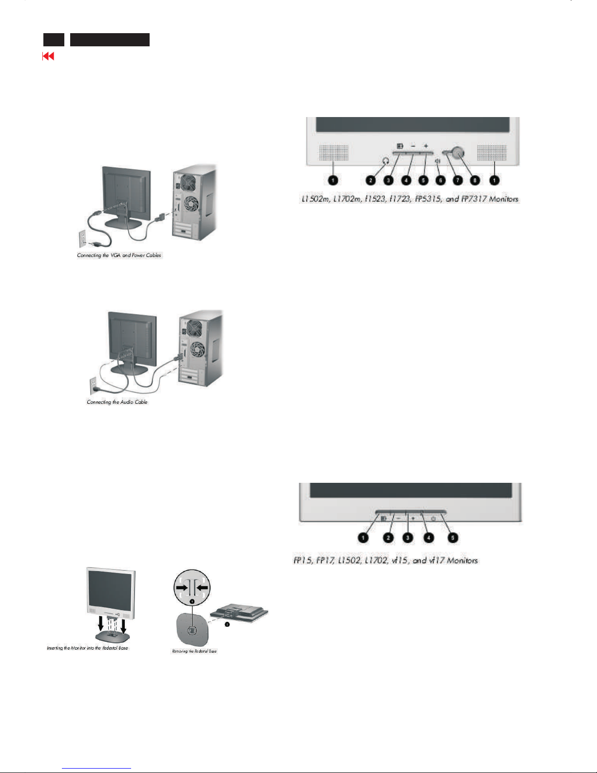
Connecting The Monitor
Go to cover page
Connecting to Your PC
1. Place the monitor in a convenient, well-ventilated location near your
computer.
2. Connect the monitor signal cable on the back of the monitor to the
video connector on the rear panel of the computer.
3. Connect one end of the power cable to the back of the monitor, and
the other end to an electrical wall outlet.
4. If your monitor is a multimedia model, connect one end of the audio
cable to the back of the monitor, and the other end to the audio
Connector on the back of the computer.
Installing the Monitor Pedestal
To install the monitor pedestal:
1. Place the pedestal plate on your desktop or table and check to
be sure the arrow on the underside of the plate is facing forward.
Do not install the base if the monitor will be used on a wall, swing arm,
or other mounting fixture; instead see the section on “Mounting the
Monitor” in this chapter.
2. Using both hands, position the monitor over the pedestal base
and press down firmly to lock the pedestal base in place. When the
base locks, it will make a clicking sound. Make sure the pedestal base
is securely locked before continuingwith the setup.
If you need to remove the pedestal base, lay the monitor down on
a soft protected surface. On the bottom side of the pedestal base,
press together the two tabs as shown in the following illustration.
This will release the pedestal from the base.
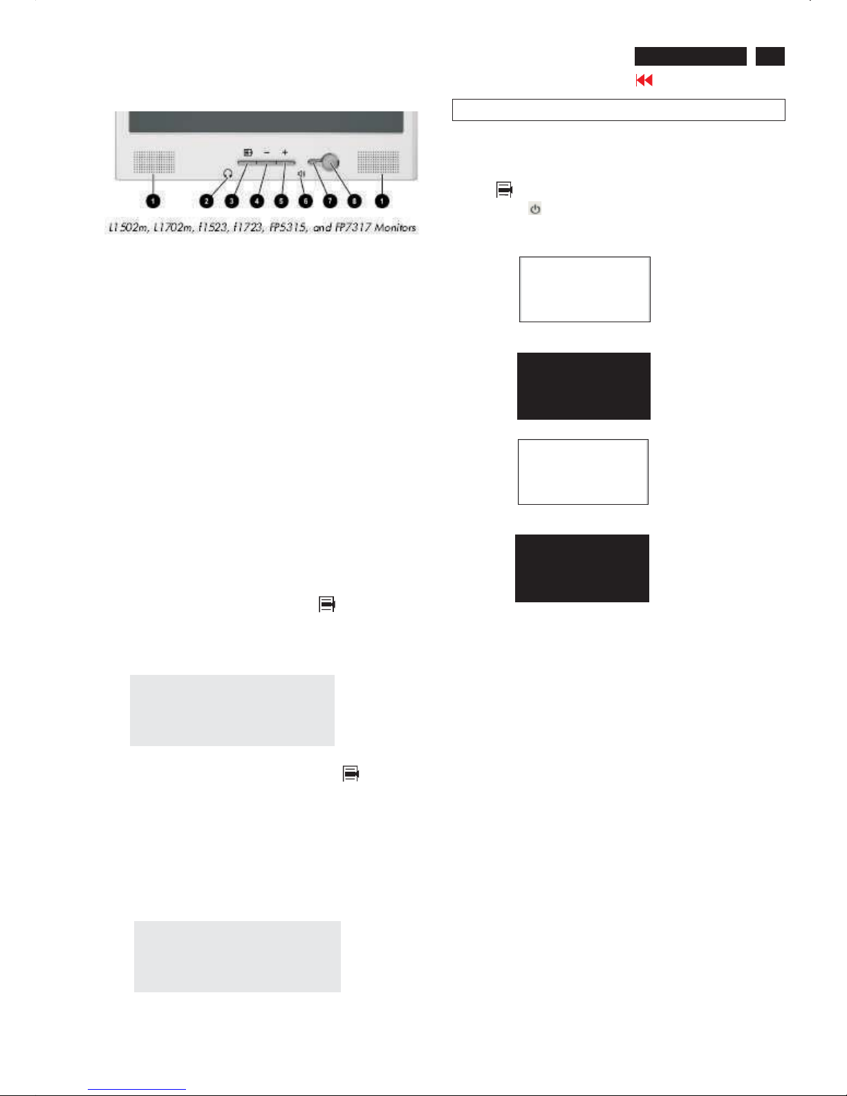
Front Panel Components
1 Speakers Audio feature for music,alarms,etc.(multimedia models only)
2 (Headphone jack)Connects a headphone set to the monitor.
3 Menu button Launches the On-Screen Display (OSD) menu and
selects functions.
4 (Minus button) When OSD is inactive, auto-adjusts the screen
Image. When OSD is active, navigates in reverse through the OSD
and adjusts OSD scale settings.
5 + (Plus button) When the OSD is active, navigates through the OSD
and adjusts OSD scale settings.
6(Volume control)Controls the volume level of the monitor speakers.
7 Power LED Fully powered = Green.
Sleep mode = Amber.
Sleep Timer mode = Flashing Amber.
8 Power Switch Powers the monitor on and off.
No. Control Function
No. Control Function
1 Menu button Launches the On-Screen Display (OSD) menu and
selects functions.
2 (Minus button) When OSD is inactive, auto-adjusts the screen
image. When OSD is active, navigates in reverse through the OSD
And adjusts OSD scale settings.
3 + (Plus button) When the OSD is active, navigates through the OSD
and adjusts OSD scale settings.
4 Power LED Fully powered = Green.
Sleep mode = Amber.
Sleep Timer mode = Flashing Amber.
5 Power Switch Powers the monitor on and off.Number Control Function
Page 5
HP L1502
5
Go to cover page
On-Screen Display
ADVANCED OSD MODE CONFIGURATION
Mode Menu
Menu Level 1 Menu Level 2 Menu Level 3 Factory Reset
Brightness ADJ Scale Y (FD = 100)
Contrast ADJ Scale Y ( FD = 50)
Image Control Auto Adjustment Show “Adjusting…” message Y (no FD)
Horizontal Position ADJ Scale Y (no FD)
Vertical Position ADJ Scale Y (no FD)
Clock ADJ Scale Y (no FD)
Clock Phase ADJ Scale Y (no FD)
Cancel
Save and Return
Color 9300 K
6500 K-sRGB Y (FD = 6500 K-
sRGB )
Custom Color R/G/B Color ADJ Y(FD =100)
Cancel
Save and Return
Language Deutsch
English N (FD=English)
Español
Français
Italiano
Nederlands
Cancel
Save and Return
Management Power Saver On / Off Selection N (FD=ON)
Power On Recall On / Off Selection N (FD=ON)
Mode Display On / Off Selection N (FD=OFF)
Sleep Timer Timer Set Menu N (FD=0;OFF)
Cancel
Save and Return
OSD Control Horizontal OSD
Position
ADJ Scale N (FD=50)
Vertical OSD
Position
ADJ Scale N (FD=50)
OSD Timeout ADJ Scale N (FD=30)
Cancel
Save and Return
Factory Reset Yes
No
Exit
Main manu
Brightness
Contrast
Image control
Color
Language
Management
OSD control
Factory reset
Exit
Pressing the Menu button ( ) the first time brings up the BASIC
menu level. The + and buttons move up and down the menu,
respectively. The selected menu function shall be highlighted in
orange text for all menus. Pressing the Menu button again brings up
the second menu level for the item selected. The selection will wrap
around if the bottom item is selected and the button is pressed, the
selection will move to the top item. Likewise, if the top item is
selected and the + button is pressed, the selection will move to the
bottom item. Selecting the “Advanced Menu” from the Basic Menu
will result in the display of the ADVANCED OSD. The Advanced
Menu will remain the default OSD upon subsequent power-ups of the
monitor until the “Basic Menu” option is selected or until “factory
reset” is selected.
Page 6
HP L1502
6
Go to cover page
Warning message table
Warning message table
BASIC OSD MODE CONFIGURATION
Mode Menu
Menu Level 1 Menu Level 2 Menu Level 3 Factory Reset
Brightness ADJ Scale Y (FD = 100)
Contrast ADJ Scale Y ( FD = 50)
Auto Adjustment Show “Adjusting… ” message Y(noFD)
Advanced Menu Refer to table 8
Exit
Item Attention Signals Display Time Condition
1 Input Signal out of Range see power saver table
2 No Input Signal see power saver table
3 Going to Sleep see power saver table
4 Adjusting… .. The Minus ( " - " ) button shall be a hot-key for the Auto-Adjustment process.
Menu button ( ), shall be hot-key for OSD Menu Exit
5 OSD Lockout 10secs Push menu key for 10 sec then display 10 sec WM “OSD Lockout”
6 Check Video Cable see power saver table
Power Saver table
Power Saver - On Power Saver - Off Note
Quit signal with cable 1. System blank and show WM 1. System blank and show
"Going to Sleep" 3 sec then sleep. moving WM "No Input Signal" always.
Disconnect cable 1. System blank and show 1. System blank and show
WM “Check Video Cable”10 WM “Check Video Cable” 10
sec then moving about 50 sec. sec then moving always.
2. Show WM “Going to
Sleep” 3 sec then sleep.
3. If push any key in sleep
mode, then repeat item 1 to 2.
Out of range –1 1. System blank and show 1. System blank and show H<29.5 or
moving WM “Input Signal moving WM “ Input Signal H>82.5 or
out of Range” 60 secs. Out of Range”always. V<49 or
2. Show WM “Going to V>87 or
Sleep” 3 sec then sleep. Vtotal>=1200
3. If push any key in sleep
mode, then repeat item 1to 2.
Out of range –2 1. Show moving WM 1. Show moving WM DownScaling
"Input Signal out of Range" 60 sec. “Input Signal out of Range”60 sec. Ex.
2. Menu key can active 2. Menu key can active 1280x1024
during moving WM and during moving WM and
operate OSD menu. operate OSD menu.
3. WM disappear if menu 3. WM disappear if menu
key push or after WM 60 sec. key push or after WM 60 sec.
Out of range –3 1. Show moving WM 1. Show moving WM 85Hz
"Input Signal out of Range" 60 sec. “Input Signal out of Range”60 sec.
2.AftermovingWM60sec 2.AftermovingWM60sec
then show WM “Going to Sleep”3 sec then show WM “Going to
then sleep. Sleep” 3 sec then sleep.
3. If push any key in sleep 3. If push any key in sleep
mode, then repeat item 1 to 2. mode, then repeat item 1 to 2.
Page 7
HP L1502
7
Go to cover page
OSD Lock/Unlock, Aging & ,
Enable/Disable "warning message"
ATTENTION
OSD LOCK OUT
Check Video Cable
To Lock/Unlock OSD function (User Mode)
-
The OSD function can be locked by pressing " " button(3) for
more than 10 seconds, the screen shows following windows for 3
seconds. Everytime when you press " " or"+"button, this
message appears on the fly screen automatically.
To Enable/Disable "Warning message" on screen
(in User Mode)
Unlock OSD function:
Locked OSD function can be released by pressing" " button for
more than 10 seconds again.
Step 1: Turn off LCD monitor, and disconnect Interface Cable
between Monitor and PC.
Step 1: Turn on LCD monitor, and disconnect Interface Cable
between Monitor and PC. bring up
Fig. 2
Bring up
After 15 seconds, bring up :
After 15 seconds, bring up :
:
After 15 seconds, bring up :
----------
---------repeatly
Connect signal cable again => go back to normal display.
Status 1.:
=> go back to Windows screen.
Connect signal cable again
Access Aging.. Mode
Step 2 :
[Push " " & " " buttons at the same time and hold it ] +
[Press power " " button untill comes out "AGING screen"
] => then release all buttons.
+
AGING...AGI N G ...
AGING...AGI N G ...
Front control panel
Fig. 1
1 Speakers Audio feature for music,alarms,etc.(multimedia models only)
2 (Headphone jack)Connects a headphone set to the monitor.
3 Menu button Launches the On-Screen Display (OSD) menu and
selects functions.
4 (Minus button) When OSD is inactive, auto-adjusts the screen
Image. When OSD is active, navigates in reverse through the OSD
and adjusts OSD scale settings.
5 + (Plus button) When the OSD is active, navigates through the OSD
and adjusts OSD scale settings.
6(Volume control)Controls the volume level of the monitor speakers.
7 Power LED Fully powered = Green.
Sleep mode = Amber.
Sleep Timer mode = Flashing Amber.
8 Power Switch Powers the monitor on and off.
No. Control Function
No. Control Function
Page 8
HP L1502
Main manu
Brightness
Contrast
Image control
Color
Language
Management
OSD control
Factory reset
Exit F
8
Go to cover page
Factory mode
Access Factory Mode
Step 2 :
[Push " " & " " buttons at the same time and hold it ] +
[Press power " " button untill comes out "Windows screen"
] => then release all buttons.
+
How to Get into Factory Mode Menu
Turn off monitor.
Press OK " " button, bring up Factory mode indication as
shown in Fig 2.
Step 1 :
Step 3 :
Basic and simple instruction on the control keys.
When you press the button on the front control of your monitor, the OnScreen Display (OSD) Main Controls window will pop up and you can
then start making adjustments to your monitor's various features.
Front control panel
Fig. 1
Fig. 2
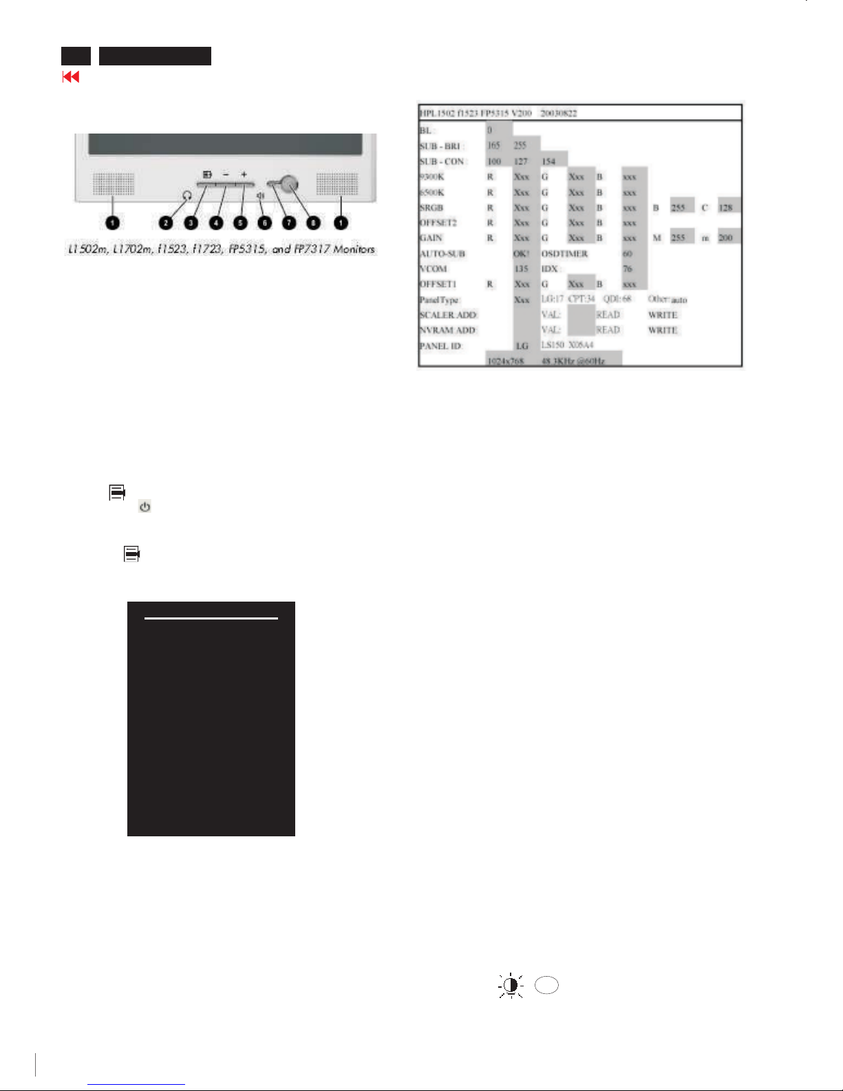
Contrast adjustment (Sub-Contrast). Use this menu item to
adjust the contrast gain of pre-amp ranges from 0 to 255.
9300KRGB
6500KRGB
Color temperature gain adjustment. Use these menu items to
adjust the RGB gains of pre-amp for different color
temperatures, ranges from 0 to 255.
OFFSET R G B
Sub-Brightness adjustment. Use this menu item to adjust
the brightness level (DC-level) of pre-amp range from 0 to
255.(R/G/B ANALOG DC -level).
GAIN R G B
R/G/B GAIN adjustment. Use this menu item to adjust
the R/G/B (GAIN) of Amp. range from 0 to 255.(R/G/B
ANALOG GAIN Values).
It is for 1024x768/60Hz with special pattern only.
AUTO SUB:
Do not use this function here.
AUTO SUB:
(PS: The OffsetRGB function can be used on reduce or eliminate
snowy noise on the background when the resolution of video signal is
1280 X 1024 vertical 60Hz. Slightly increase or decrease the value
until snowy noise completely disappear.)
Hot key function: by pressing "UP" and "DOWN" key
simultaneously at User mode (or Factory mode).
-
OK
-
SUB CON:SUB CON:
BL : Blacklevel value
SUB-BRI : Brightness value range(Min Max). Fix value for
continue mode requirement.LG(Min=165, Max=255),
CPT(Min=165, Max=230), QDI(Min=165, Max=225).
SUB-CON : Contrast value range(Min Mid Max)
SRGB-B : Brightness of sRGB(Reserved)
SRGB-C : Contrast of sRGB(Reserved)
Gain-m : Minimum value of User Gain
Gain-M : Maximum value of User Gain
AUTO-SUB: To do Auto color function when push "Up" key in
White pattern
OSDTIMER : OSD time out control (sec) Unused in this project
VCOM : For LG panel control
IDX : Limit current of inverter(Fix value QDI: 76, CPT: 45, LG:5)
Panel Type: If set this to 17, 34 or 68 then system will force panel
type to LG, CPT or QDI. Set to other value will auto
detect panel based on panel hardware.
SCALER : Read/Write scaler register
NVRAM : Read/Write eeprom address
Factory menu
Cursor can move on gray color area
Fig. 3
<------Factory mode indicator
Page 9
9
HP L1502
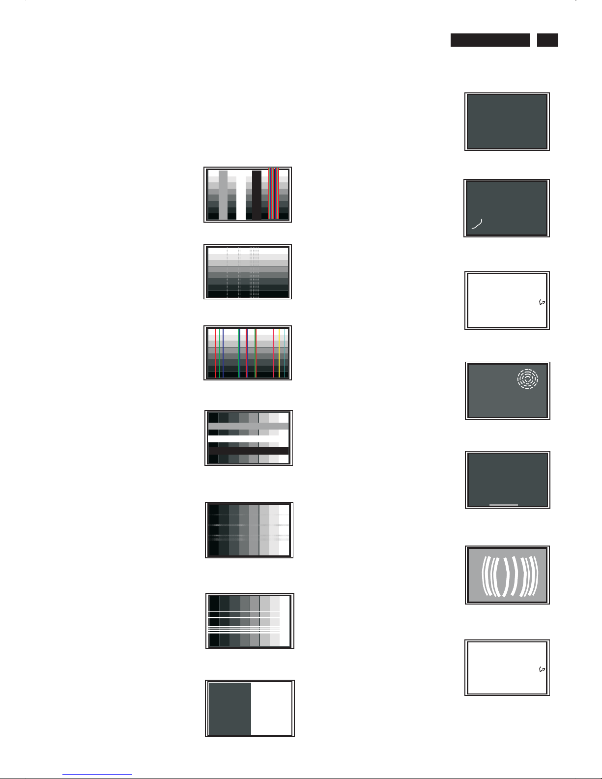
Failure Mode of LCD panel
Quick reference for failure mode of LCD panel
This page presents problems that could be made by LCD panel. It is
not necessary to repair circuit board. Simply follow the “Mechanical
instruction” on this manual to eliminate failure by replace LCD panel
or backlight tubes.
Failure description Phenomenon
Vertical dim lines
Vertical block defect
Vertical lines defect
(Always bright or dark)
Horizontal block defect
Horizontal dim lines
Horizontal lines defect
(Always bright or dark)
Has bright or dark pixel
.
..
.
.
.
.
..
.
.
.
Bright pixel
Dark pixel
..
. .. .
Polarizer has bubbles
Polarizer has bubbles
Foreign material inside
polarizer. It shows linear or
dot shape.
. .. .
Concentric circle formed
Bottom back light of LCD is
brighter than normal
Backlight un-uniformity
Backlight has foreign
material. Black or white
color, linear or circular type
9
Go to cover page
Page 10

HP L1502
10
Troubleshooting
Go to cover page
Solving Common Problems
The following table lists possible problems, the possible cause of each problem, and the recommended solutions.
Screen is blank. Power cord is disconnected. Connect the power cord.
Power switch is turned Off. Turn on the power.
Video cable is improperly connected. Connect the video cableproperly.
Screen blanking utility is active. Depress any key on the keyboard or move
The mouse to inactivate the screen blanking
Utility.
Problem Possible Cause Solution
Image appears
blurred, indistinct, or
Too dark.
Image is not
Centered. auto-adjust the screen image.
Press the Menu button to access the
Advanced OSD menu. Select Image
Control/Horizontal Position or Vertical
Position to adjust the horizontal or vertical
position of the image.
Check Video
Cable is displayed
on screen.
(Input Signal Out of
Range) is displayed
on screen.
Restart your computer so that the
new settings take effect.
Brightness and contrast Press the Minus button on
are too low. the monitor front panel to
auto-adjust the screen. If that
Does not work, press the
Menu button to open the
Basic OSD Menu, and
adjust the brightness and
contrast scales as needed.
Position may need When OSD is inactive,press-(minus
Adjustment. button) to
Monitor video cable is Connect the 15-pin monitor video cable
disconnected. to the VGA connector on the computer.
Be sure that the computer
power is off while: connecting the video
Cable.
Video resolution and/or Restart your computer and enter Windows
refresh rate are set Safe Mode by pressing the F6 Function
higher than what your key when the computer starts to boot up.
monitor supports. Change your settings to a supported
setting.
Page 11
HP L1502
11
Go to cover page
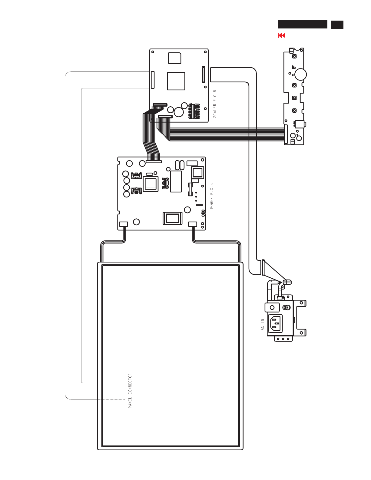
Wiring Diagram
Page 12

HP L1502
12
Go to cover page
Flat Panel Adjust
Optimizing Performance
Installing FPadjust Program
For best performance, ensure that your display settings are set at 1024x768@60Hz (for
14"/15") or 1280x1024, 60Hz (for 17"/18").
Note: You can check the current display settings by pressing the 'OK' button once. Go into the
Product Information.
The current display mode is shown on the item called RESOLUTION.
You can also install the Flat Panel Adjust (FP Adjust) program, a program for getting the best
performance out of your monitor. This included on this CD. Step-by-step instructions are
provided to guide you through the installtion process. Click on the link to know more about this
program.
The FP Adjust program generates alignment patterns which will help you adjust monitor
settings such as CONTRAST, BRIGHTNESS, HORIZONTAL & VERTICAL POSITION, PHASE
and CLOCK.
System requirements:
PC running Windows 95, Windows 98, Windows 2000, Winodws Me, Windows XP or later
To install FPadjust Program:
Click on the link or icon to install FPadjustment Program.
or
Click-and-hold your mouse over the icon. (Win95/98/2000/Me/XP users right-click)
Download FP_setup04.exe
From the menu that appears, choose 'Save Link As...', 'Save Target As...' or 'Download Link to
Disk'.
Choose where you would like to save the file; click 'Save' (if prompted to save as either 'text'
or 'source', choose 'source'). Exit your browser and install the FPadjust Program. Read the
"FP_Readme04.txt" file before installing.
Page 13

170C4/N4
13
Go to cover page
Definition of Pixel Defects
LCD Monitor Quality and Pixel Policy
The TFT monitor uses high-precision technology, manufactured according to HP
standards, to guarantee trouble-free performance. Nevertheless, the display
may have cosmetic imperfections that appear as small bright or dark spots. This
is common to all LCD displays used in products supplied by all vendors and is not
specific to the HP LCD. These imperfections are caused by one or more
defective pixels or sub-pixels.
1. A pixel consists of one red, one green, and one blue sub-pixel.
2. A defective whole pixel is always turned on (a bright spot on a dark
background), or it is always off (a dark spot on a bright background). The first
is the more visible of the two.3. Adefective sub-pixel (dot defect) is less
3. visible than a defective whole pixel
and is small and only visible on a specific background.
The HP display does not have more than:
4. 3 bright dots.
5. 5 dark dots.
6. 5 total bright and dark dots.
7. No more than two adjacent (less than 2.5 mm edge-to-edge)
defective pixels.
To locate defective pixels, the monitor should be viewed under normal operating
conditions, in normal operating mode at a supported resolution and refresh rate,
from a distance of approximately 50 cm (16 in.).
HP expects that, over time, the industry will continue to improve its ability to
produce LCDs with fewer cosmetic imperfections And HP will adjust guidelines
as improvements are made.
Page 14
HP L1502
14
Go to cover page
Mechanical Instructions
Front view-HP L1523
Fig. 1
Fig. 2
Fig. 3
Step 1. Remove the Base as Fig .3
Remove the four screws of Fig. 4.Back cover as
Step 2.Remove the
Use the thin "I" type screw driver to open the clicks as Fig.5~7.
back cover
Fig. 4
Back view
Fig.5
Fig.6
Step 3. Remove the 13 screws
And Disconnect the 4 cables as Fig.8
Base =====>
Four screws
=====>
=====>
=============>
============>
Botton view
Right and Left view
Fig.7
Top view
=====>
=====>
=====>
=====>
=====>
=====>
=====>
=====>
===>
=====>
=====>
Fig.8
=====>
4 Cables
===>
===========>
Fig.9
Step 4. Disconnect the 2 cables as Fig.9
2 cables===>
========>
Page 15
HP L1502
15
Go to cover page
Mechanical Instructions
Remove the Scaler and Power board as Fig. 10.
Fig. 11
Fig. 12
Step 6. Remove the Front Bezel
Use the thin "I" type screw driver to open the clicks
as Fig.13 &14.
Fig. 10
Fig. 13
Fig. 15
***************************************************************************
In warranty, it is not allowed to disassembly the LCD panel, even the
backlight unit defect.
Out of warranty, the replacment of backlight unit is a correct way
when the defect is cused by backlight (CCFL,Lamp).
***************************************************************************
Step 5. Remove the control board
Remove the seven screws and cable as Fig. 11 & 12.
Scaler board
Power board
Cable
======>
Fig. 14
1050 9322 196 43682 TFT-LCD LS150X05 (LGPH)
1050 9322 195 10682 TFT-LCD CLAA150XG08 (CPT0)
======>
======>
======>
======>
Page 16
16
HP L1502
Go to cover page
Safety Test Requirements
All units that are returned for service or repair must pass the
original manufactures safety tests. Safety testing requires both
and testing.Hipot Ground Continuity
HI-POT TEST INSTRUCTION
1. Application requirements
2. Test method
1.1 All mains operated products must pass the Hi-Pot test as
described in this instruction.
1.2 This test must be performed again after the covers have
been refitted following the repair, inspection or modification
of the product.
2.1 Connecting conditions
2.1.1 The test specified must be applied between the parallel-
blade plug of the mainscord and all accessible metal
parts of the product.
2.1.2 Before carrying out the test, reliable conductive
connections must be ensured and thereafter be
maintained throughout the test period.
2.1.3 The mains switch(es) must be in the "ON" position.
2.2 Test Requirements
All products should be HiPot and Ground Continuity tested as
follows:
Test 2820VDC 1700VDC Test current:
voltage (2000VAC) (1200VAC) 25A,AC
Test time:
Test time 3 seconds 1 second 3 seconds(min.)
(min.) Resistance
required:
Trip set at 100 uA 5 mA <=0.09+R ohm,
current for Max. R is the
(Tester) limitation; set resistance of
at 0.1 uA for the mains cord.
Min. limitation
Ramp set at 2
time seconds
Condition HiPot Test for HiPot Test for Ground Continuity
products where products where Test requirement
the mains input the mains input is
range is Full 110V AC(USA
range(or 220V type)
AC)
2.2.1 The test with AC voltage is only for production purpose,
2.2.2 The minimum test duration for Quality Control Inspector
must be 1 minute. No breakdown during the test.
2.2.3 The test voltage must be maintained within the specified
voltage + 5%.
2.2.4 The grounding blade or pin of mains plug must be
conducted with accessible metal parts.
Service center shall use DC voltage.
3. Equipments and Connection
4. Recording
3.1. Equipments
For example :
- ChenHwa 9032 PROGRAMMABLE AUTO SAFETY
TESTER
- ChenHwa 510B Digital Grounding Continuity Tester
- ChenHwa 901 (AC Hi-pot test), 902 (AC, DC Hi-pot test)
Withstanding Tester
3.2. Connection
Hipot and Ground Continuity testing records have to be kept for
a period of 10 years.
* Turn on the power switch of monitor before Hipot and
Ground Continuity testing.
Connect the "video cable"
or "grounding screw"
to the CLIP on your tester.
Video cable
(Rear view of monitor)
Connect the power cord
to the monitor.
Grounding screw
Power outlet
(ChenHwa 9032 tester)
Clip
Clip
Page 17
HP L1502
17
Electrical Instructions
Go to cover page
1.
1.1 During the test and measuring, supply a distortion free AC mains
voltage To the apparatus via an isolated transformer with low
internal resistance.
1.2 All measurements mentioned hereafter are carried out at a normal
mains voltage (90 - 132 VAC for USA version, 195 -264 VAC for
EUROPEAN version, or 90 - 264 VAC for the model with full range
power supply, unless otherwise stated.)
1.3 All voltages are to be measured or applied with respect to ground,
unless otherwise stated.
Note: don't use heat-sink as ground.
1.4 The test has to be done on a complete set including LCD panel
after 30 minutes warm-up at least in a room with temperature of 25
+/- 5 degree C.
1.5 All values mentioned in this test instruction are only applicable of a
well aligned apparatus, with correct signal.
1.6 The letters symbols (B) and (S) placed behind the test instruction
denotes (B): carried out 100% inspection at assembly line
(S): carried out test by sampling
1.7 The white balance (color temperature) has to be tested in subdued
lighted room.
1.8 Repetitive power on/off cycle are allowed except it should be
avoided within 6 secretary.
2.1 Signal type
Video: 0.7 Vpp linear, positive polarity
Sync. : TTL level, separate, positive or negative polarity
Reference generator: CHROMA 2200 or 2250
Allowed signal modes list: Table A
General points
Input signal2.
TABLE A
FACTORY PRESET DISPLAY MODES
Pixel
Format
Horz
Freq
(KHz)
Horz
Polarity
Vert
Freq
(Hz)
Vert
Polarity
Pixel
Clk
(MHz)
1 640 x 480 31.469 - 59.940 - 25.175 VGA
2 640 x 480 37.861 - 72.809 - 31.500 VESA
3 640 x 480 37.500 - 75.000 - 31.500 VESA
4 720 x 400 31.469 - 70.087 + 28.322 VGA
5 800 x 600 37.879 + 60.317 + 40.000 VESA
6 800 x 600 48.077 + 72.188 + 50.000 VESA
7 800 x 600 46.875 + 75.000 + 49.500 VESA
8 832 x 624 49.726 +/- 74.551 +/- 57.284 MAC
9 1024 x
768
48.363 - 60.004 - 65.000 VESA
10 1024 x
768
56.476 - 70.069 - 75.000 VESA
11 1024 x
768
60.023 + 75.029 + 78.750 VESA
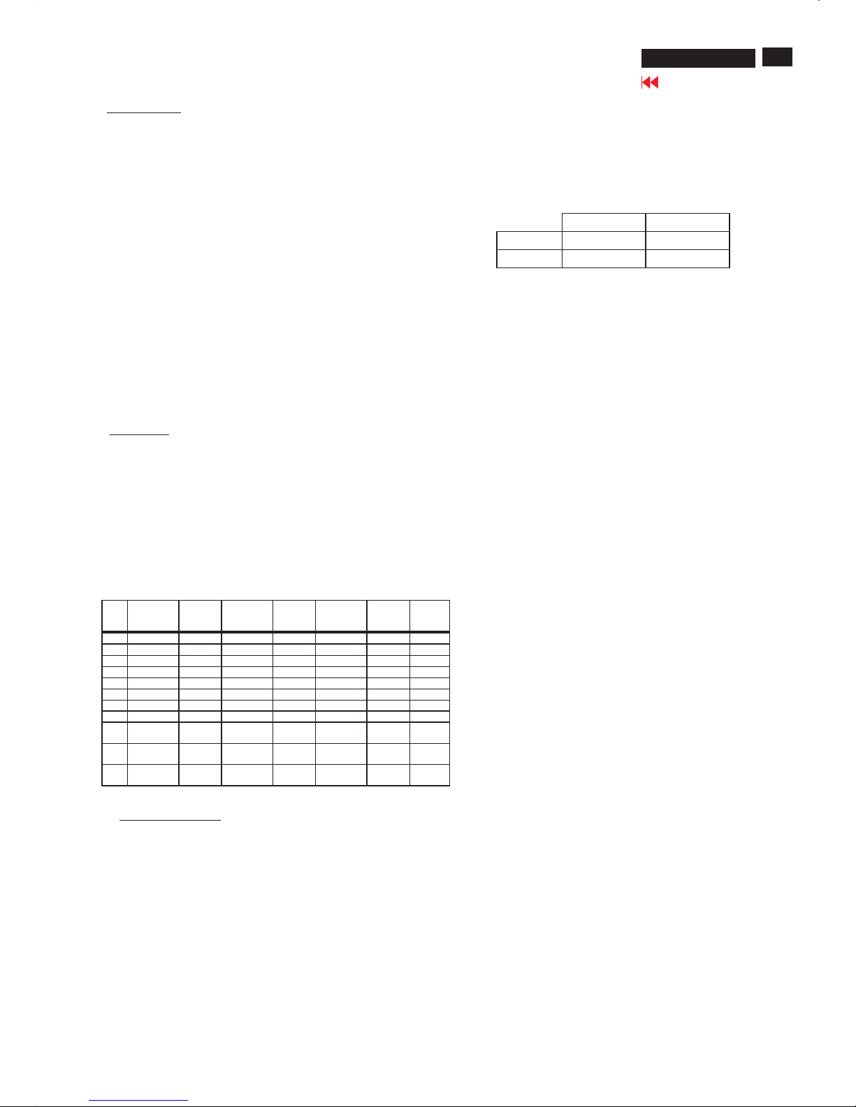
3. Display Adjustment (B)
Access to factory mode. Check “CPU version”, if it is not right
version, then ISP new one (7301). After pre-check, aging 1 hour at
Least. Programming Analog DDC Data into Monitor.
3.1 Panel flicker adjustment (B)
Apply a 48kHz/60Hz signal with green pixel on/off at 128/256-level
pattern for LG panel. Set brightness control at 100%, and contrast
control at 50%, adjust GPIO1 of 7443 GM2116AA which is on
scaler board to make panel's flicker minimum.
3.2 Auto color adjustment
Apply a 48.36kHz/60Hz signal with white pattern.
Set brightness at 100% and contrast at 80%.
Using auto color, let scaler calibrate offset1,offset2 and gain itself.
** Check the 64-gray level is distinguishable.
3.3 Color temperature adjustment
Apply a 48.36kHz / 60Hz signal with white pattern.
Set brightness control at 100% and contrast control at 50%.
Adjust the R.G.B gain to reach special color temperature on
center of screen. Keep one color fixed gain to maximum at least.
The 1931 CIE chromaticity (x, y) coordinates shall be:
Use Minolta CA-110 for color coordinates and luminance check.
3.4 NVRAM(24C16) Default Values
Sub_Bri: 165 255/LG 230/CPT 225/QDI
Sub_Con: 100 127 154
VCOM: 152
3.5 Factory Reset
After finishing all the adjustment, select “Factory Reset” function
to recall:
Do an automatic Auto-Adjustment
Set Brightness = 100
Set Contrast = 50
Set Color = 6500K-sRGB
Set Custom Color (R.G.B) = 100
3.6 Main Menu Factory Default Values
The OSD shall have the following factory default values:
Language = English
OSD Cotrol:
Horizontal OSD position = 50
Vertical OSD position = 50
OSD timeout = 30s
Management:
Power Saver = ON
Power On Recall = ON
Mode display = OFF
Sleep Timer = OFF
Menu = BASIC
9300°K 6500°K-sRGB
x (center) 0.283 ± 0.005 0.313 ± 0.005
y (center) 0.297 ± 0.005 0.329 ± 0.005
Page 18
18
HP L1502
Display Adjustment
Display Adjustment:
Press and button simultaneously while power ON.
Adjust OSD menu to lower position of screen (i.g. adjust OSD HPosition and OSD V-Position to 0 at OSD setup sub-menu. Then
press or button to move the cursor to
item ( see yellow circle on table 1). Press button to access
to factory mode (see table2.). Check the code of CPU version if it
is not right version, then ISP new one (7301). After pre-check,
aging 1 hour at least. Programming Analog DDC data into
Monitor. Check # serial number to meet bar code label.
+
Down Up Factory Entrance
Menu
Table 2. The content of Factory setting.see table 2.
Cursor can move on gray color area
1. Auto color adjustment:
Apply a 48.36kHz/60Hz signal with white pattern. Set brightness
at 100% and contrast at 50%. Move the cursor by pressing or
button to ( see red circle on table 2 ), press OK
button to do auto color, scaler would calibrate offset1,offset2 and
gain itself then display OK. Check the 64-gray level is
distinguishable.
Up
Down AutoColor
Table 1.
2. Color temperature adjustment:
Apply a 48.36kHz / 60Hz signal with white pattern.Set brightness
control at 100% and contrast control at 50%. Adjust the R.G.B
gain to reach special color temperature on center of screen.
Keep one color fixed gain to maximum at least.
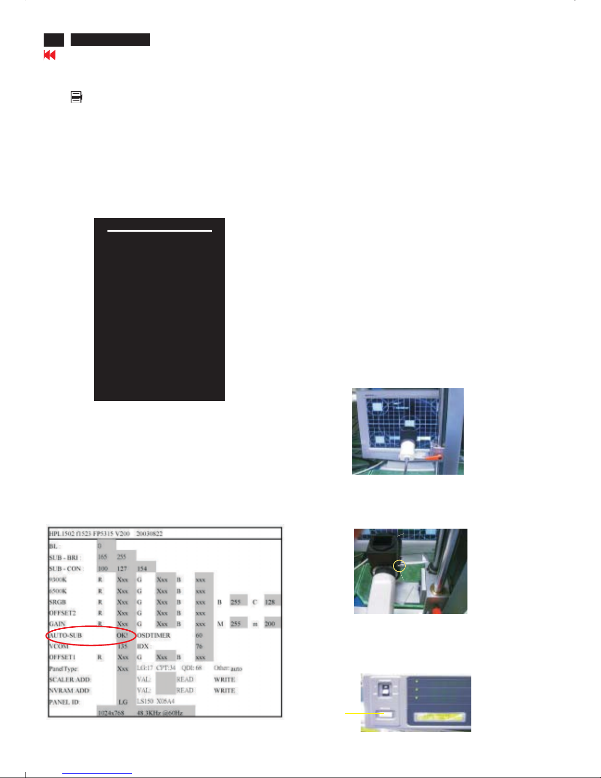
2 .1 Aim the probe CA-A30 at the center of screen as Fig. 1
2 .2 Remove the lens protective cover of probe CA-A30.
2 .3 Set Measuring/viewing selector to Measuring position for reset
analyzer. (Zero calibration) as Fig. 2
2 .4 Turn on the colour analyzer (CA-110).
2 .5 Press 0-CAL button to start reset analyzer. See Fig.3
Table 2.
Measurement/viewing selectorMeasurement/viewing selector
cover (black)cover (black)
Fig. 1
Fig. 2
Fig. 3
0-CAL
Go to cover page
Main manu
Brightness
Contrast
Image control
Color
Language
Management
OSD control
Factory reset
Exit F
<-------------Factory mode indicator
<------Version of code indicator
Page 19
19
HP L1502
Display Adjustment
2.6 Switch light probe to Viewing position.
2.7 Move the Lens barrel forward or backward to get clear image as
shown in Fig. 4
2.8 Switch light probe to Measuring position. It should be able to
indicate colour value on the CA-110.
Measurement/viewing selectorMeasurement/viewing selector
Fig. 4
Clear image
2.9 Press buttons to selectRGBof9300 and 6500.
Increase / decrease value by press or buttons until the
1931 CIE chromaticity ( x,y)asbelow.
Menu
Up Down
Alignment hits:
1. R for x value , G for y value, B for Y value on the colour analyzer.
2. Must to select 9300 in user mode, then 9300 is available in factory
Mode.
3. Must to select 6500 in user mode, then 6500 is available in factory
Mode.
3. NVRAM(24C16) Default Values:
Sub_Bri: 165 255/LG 230/CPT 225/QDI
Sub_Con: 100 127 154
VCOM: 152
4. Factory Reset:
After finishing all the adjustment, select “Factory Reset” function
to recall:
Do an automatic Auto-Adjustment
Set Brightness = 100
Set Contrast = 50
Set Color = 6500K-sRGB
Set Custom Color (R.G.B) = 100
To leave factory mode by restart the monitor.
9300°K 6500°K
x (center) 0.283 ± 0.020 0.313 ± 0.020
y (center) 0.297 ± 0.020 0.329 ± 0.020
5. EEPROM Presetting:
6.Main Menu Factory Default Values
After finishing all the adjustment,Set:
Brightness control to 100%
Contrast control to 50%
OSD position at middle of screen.
Color Adjust to 6500K color.
When adjustment is finished,monitor should be set to 6500K.
The OSD shall have the following factory default values:
Language = English
OSD Cotrol:
Horizontal OSD position = 50
Vertical OSD position = 50
OSD timeout = 30s
Management:
Power Saver = ON
Power On Recall = ON
Mode display = OFF
Sleep Timer = OFF
Go to cover page
Page 20
PIN MNEMONIC SIGNAL
1 RV Red Video
2 GV Green Video/Sync on Green
3 BV Blue Video
4 NC None
5 GND Ground (DDC Return) or Cable detect
6RGRedGND
7GGGreenGND
8BGBlueGND
9+5V+5V
10 SG Sync GND or Cable detect
11 NC None
12 SDA DDC Data
13 HS Horizontal Sync
14 VS Vertical Sync
15 SCL DDC Clock
Go to cover page
X
20
HP L1502
DDC Instructions
General
Pin assignment
A. 15-pin D-Sub Connector
DDC Data Re-programming
Analog DDC IC, & EEPROM
Additional information
In case the DDC data memory IC or main EEPROM which storage all
factory settings were replaced due to a defect, the serial numbers have
to be re-programmed" ".
It is advised to re-soldered DDC IC and main EEPROM from the old
board onto the new board if circuit board have been replaced, in this
case the DDC data does not need to be re-programmed.
Additional information about DDC (Display Data Channel) may be
obtained from Video Electronics Standards Association (VESA).
Extended Display Identification Data(EDID) information may be also
obtained from VESA.
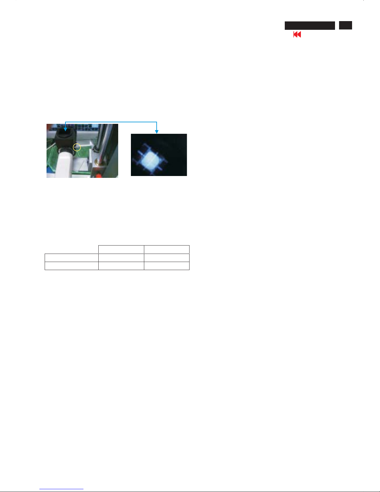
1. An i486 (or above) personal computer or compatible.
2. Microsoft operation system Windows 95/98 .
Y o Install the EDID_PORT_Tool under Win2000/XP . As
Fig. 1 .
A. Cody the "UserPort.sys" to C:\WINNT\system32\drivers(win2000)
C:\WINDOWS\system32\drivers(winXP)
B. Running " io.exe" everytime, Before you start to programming
edid data .
4. A/D Alignment kits (3138 106 10079):
inclusion : a. Alignment box x1 (as Fig. 2)
b. Printer cable x1
c. (D-Sub) to (D-Sub) cable x1
Note: The EDID45.EXE is a windows-based program, which cannot
be run in MS-DOS.
System and equipment requirements
ou have t
3. EDID45.EXE program .
Note: The alignment box has already build-in a batteries socket for
using as power source. Pull out the socket by
remove four screws at the rear of box. Please do not forget that
remove batteries after programming. The energy of batteries can
only drive circuits for a short period of time.
batteries (5V)
Fig. 2Fig. 2
Fig. 1Fig. 1
1
5
6
10
11
15
To Monitor
D-sub cable
DC 5V
To Printer port
Power
indicator
Fig. 3Fig. 3
Page 21

X
Go to cover page
21
HP L1730
DDC Instructions
21
HP L1502
Step 3: Installation of EDID45.EXE
Method 1: Start on DDC program
Start Microsoft Windows.
1. The Program"EDID45.EXE" in service manual cd-rom be copyed to
C:\ .
2. Click , choose Run at start menu of Windows as shown in
Fig. 4.
Fig. 4
4. Click button. The main menu appears (as shown in Fig. 6).OK
This is for initialize alignment box.
Fig. 6
Fig. 5
Fig. 7
Note 1: If the connection is improper, you will see the following error
message (as shown in Fig. 7) before entering the main menu.
Meanwhile, the (read EDID) function will be disable. At this time,
please make sure all cables are connected correctly and fixedly,
and the procedure has been performed properly.
3. At the submenu, type the letter of your computer's hard disk drive
followed by :EDID45 (for example, C:\EDID45, as shown in Fig. 5).
Method 2: After create a shortcut of EDID45.EXE
This is for initialize alignment box.
: Double click EDID45 icon (as shown in Fig. 8) which is
on the screen of Windows Wallpaper.
Bring up main menu of EDID45 as shown in Fig. 9.
Fig. 9
Note 2: During the loading, EDID45 will verify the EDID data which just
loaded from monitor before proceed any further function, once
the data structure of EDID can not be recognized, the following
error message will appear on the screen as below. Please
confirm following steps to avoid this message.
1. The data structure of EDID was incorrect.
2. DDC IC that you are trying to load data is empty.
3. Wrong communication channel has set at configuration setup
windows.
4. Cables loosed or poor contact of connection.
Fig. 8
1
Configuration and procedure
There are 2 chips contained OSD string, serial number..etc
on the circuit board, main EEPROM which storage all factory
settings,OSD string. DDC IC which storage 128byte EDID data(serial
number ..etc.). Following descirptions are the connection and procedure
for Analog and main EEPROM can be re-programmed along with
Analog/Digital IC by enable factory memory data write function on the
DDC program (EDID45.EXE).
Initialize alignment box
In order to avoid that monitor entering power saving mode due
to sync will cut off by alignment box, it is necessary to initialize
alignment box before running programming software
(EDID45.EXE). Following steps show you the procedures and
connection.
Step 1: Supply 5V DC power source to the Alignment box by plugging a
DC power cord or using batteries.
Step 2: Connecting printer cable and D-Sub cable of monitor as Fig. 3
Fig. 3
PC
1=Power connector
2=D-SUB connector
~
~
To printer port (LTP1)
DC Power
5V
Printer
Port
To
Monitor
To P C
1
2
----->
----->
Fig. 10
Page 22

X
Go to cover page
21
HP L1730
DDC Instructions
22
HP L1502
Re-programming Analog DDC IC
Step 1: After initialize alignment box, connecting all cables and
box as shown in Fig. 11
Fig. 12
Step 2: Read DDC data from monitor
1. Click icon as shown in Fig. 12 from the tool bar to bring up
the Channels "Configuration Setup" windows as shown in Fig. 13.
Step 3: Modify DDC data (verify EDID version, week, year)
1. Click (new function) icon from the tool bar, bring up
Step 1 of 9 as shown in Fig. 15 .
EDID45 DDC application provides the function selection and
text change (select & fill out) from Step 1 to Step 9.
Step 4: Modify DDC data (Monitor Serial No.)
Next1. Click , bring up Fig. 16.
2. Click , bring up Fig. 17.Next
3. Click OK button to confirm your selection.
4. Click icon (Read EDID function) to read DDC EDID data from
monitor. The EDID codes will display on screen as shown in Fig. 14.
Fig. 16
Fig. 17
2. Select the DDC2Bi as the communication channel.
As shown in Fig. 13.
Fig. 14
Fig. 15
Fig. 11
1=Power connector
2=D-SUB connector
~
~
PC
To printer port (LTP1)
DC Power
5V
Printer
Port
To
Monitor
To P C
1
2
----->
----->
Don't close this screen. --->
Fig. 13
To PC Video port (D-sub)
Select and fill out,
If necessary.
Page 23

X
Go to cover page
21
HP L1730
DDC Instructions
23
HP L1502
Fig. 18
Fig. 22
Fig. 19
Fig. 20
3. Click , bring up Fig. 18.Next
7. Click , bring up Fig. 22.Next
4. Click , bring up Fig. 19.Next
5. Click , bring up Fig. 20.Next
Fig. 23
8. Click , bring up Fig. 23.Next
- Serial number can be filled up or be changed at this moment.
- Click to exit the Step window.Finish
Fig. 21
------>
6. Click , bring up Fig. 21.Next
Pls. See next page for serial
number indication
Page 24

X
Go to cover page
21
HP L1730
DDC Instructions
24
HP L1502
PSG Serial number for HP system
The format for the serial number is as follows:
\/ | | \/ \| / /
ABCD E
A: Country of Manufacture Code
The country of manufacture code is based on the ISO
International country code standard (ISO # 3166, Alpha-2
code) and is used to designate the specific country of
manufacture. The same product can be manufactured in
more than one country.
B: Manufacturer Code
This code is corresponds to the type of panel being used
for the units. This digit as the following value :
C: Year
Corresponds to year of manufacture. For example,
year 1998, use the least significant digit 2 to designate
Year of manufacture.
D: Week
Corresponds to 01 - 52 week of manufacture.
E: Combine alphabets with digits depended on panel
For panel : B000~BZZZ, C000~CZZZ, D000~DZZZ
For panel: F000~FZZZ, G000~GZZZ, H000~HZZZ
For panel: J000~JZZZ, K000~KZZZ, L000~LZZZ
For panel: M000~MZZZ, N000~NZZZ, P000~PZZZ
Skip 5 letters A, E, I, O AND U.
C C PY W W NNNN
TW: TAIWAN
CN: CHINA
P: PHILIPS
LPL
CPT
HSD
QDI
Reset counter each week.
Step 7: Save DDC data
Sometimes, you may need to save DDC data as a text file for using
in other IC chip. To save DDC data, follow the steps below:
1. Click (Save) icon (or click "file"-> "save as") from the tool bar
And give a file name as shown in Fig. 25.
The file type is EDID45 file (*.ddc) which can be open in WordPad.
By using WordPad, the texts of DDC data & table (128 bytes, hex
code) can be modified. If DDC TEXTS & HEX Table are completely
correct, it can be saved as .ddc flie to re-load it into DDC IC for DDC
Data application.
2. Click .Save
Step 8: Exit DDC program
Pull down the File menu and select Exit as shown in Fig. 26.
Step 6: Write DDC data
1. Configuration should be as Fig. 24. And press OK.
2. Click (Write EDID) icon from the tool bar to write DDC data.
Bring up "Writing 0%~100%, ready" a progressing bar on the left
down corner.
3. Click (Read EDID) to confirm it.
4. Press the OK button to bring up the osd main manu.
5. Press the DOWN button to select PRODUCTION INFORMATION
press the OK button to confirm our selection.
6. Re-confirm the serial Number is updated.
Fig. 24
Fig. 26
Fig. 25
HP L1502-DDC-CPT
C:\My documents\HP L1502-DDC-CPT
Edid45Files
Page 25

HP L1502
25
Go to cover page
DDC Instructions
THE DISPLAY DATA CHANNEL ( DDC ) 2B CONTENT
(FOR analog)
Vendor/Product Identification
ID Manufacturer Name : HWP
ID Product Code : 2600 (HEX.)
ID Serial Number : B001 (HEX.)
Week of Manufacture : 25
Year of Manufacture : 2003
EDID Version, Revision
Version : 1
Revision : 3
Basic Display Parameters/Features
Video Input Definition : Analog Video Input
0.700V/0.000V (0.70Vpp)
without Blank-to-Black Setup
Separate Sync
without Composite Sync
without Sync on Green
no Serration required
Maximum H Image Size : 30
Maximum V Image Size : 22
Display Transfer Characteristic : 2.2
(gamma)
Feature Support (DPMS) : Standby
Suspend
Active Off
Display Type : RGB color display
Preferred Timing Mode : Detailed timing block 1
Color Characteristics
Red X coordinate : 0.635
Red Y coordinate : 0.343
Green X coordinate : 0.302
Green Y coordinate : 0.581
Blue X coordinate : 0.145
Blue Y coordinate : 0.096
White X coordinate : 0.313
White Y coordinate : 0.329
Established Timings
Established Timings I : 720 x 400 @70Hz (IBM,VGA)
640 x 480 @60Hz (IBM,VGA)
640 x 480 @72Hz (VESA)
640 x 480 @75Hz (VESA)
800 x 600 @60Hz (VESA)
Established Timings II : 800 x 600 @72Hz (VESA)
800 x 600 @75Hz (VESA)
832 x 624 @75Hz (Apple,Mac II)
1024 x 768 @60Hz (VESA)
1024 x 768 @70Hz (VESA)
1024 x 768 @75Hz (VESA)
Manufacturer's timings :
Standard Timing Identification #1
Horizontal active pixels : 1024
Aspect Ratio : 4:3
Refresh Rate : 60
Detailed Timing #1
Pixel Clock (MHz) : 65
H Active (pixels) : 1024
H Blanking (pixels) : 320
V Active (lines) : 768
V Blanking (lines) : 38
H Sync Offset (F Porch) (pixels) : 24
H Sync Pulse Width (pixels) : 136
V Sync Offset (F Porch) (lines) : 3
V Sync Pulse Width (lines) : 6
H Image Size (mm) : 300
V Image Size (mm) : 220
H Border (pixels) : 0
V Border (lines) : 0
Flags : Non-interlaced
: Normal Display, No stereo
: Digital Separate sync.
: Negative Vertical Sync.
: Negative Horizontal Sync.
Monitor Descriptor #2
Monitor Range Limits
Min. Vt rate Hz : 56
Max. Vt rate Hz : 76
Min. Horiz. rate kHz : 30
Max. Horiz. rate kHz : 61
Max. Supported Pixel : 80
No secondary GTF timing formula supported.
Monitor Descriptor #3
Monitor Name : hp L1502
Monitor Descriptor #4
Serial Number : CNP325B001
Extension Flag : 0
Check sum : E3 (HEX.)
**********************************************************************
EDID data (128 bytes)
**********************************************************************
0: 00 1: ff 2: ff 3: ff 4: ff 5: ff 6: ff 7: 00
8: 22 9: f0 10: 00 11: 26 12: 01 13: b0 14: 00 15: 00
16: 19 17: 0d 18: 01 19: 03 20: 68 21: 1e 22: 16 23: 78
24: ea 25: b7 26: 25 27: a2 28: 57 29: 4d 30: 94 31: 25
32: 18 33: 50 34: 54 35: ad 36: ee 37: 00 38: 61 39: 40
40: 01 41: 01 42: 01 43: 01 44: 01 45: 01 46: 01 47: 01
48: 01 49: 01 50: 01 51: 01 52: 01 53: 01 54: 64 55: 19
56: 00 57: 40 58: 41 59: 00 60: 26 61: 30 62: 18 63: 88
64: 36 65: 00 66: 2c 67: dc 68: 10 69: 00 70: 00 71: 18
72: 00 73: 00 74: 00 75: fd 76: 00 77: 38 78: 4c 79: 1e
80: 3d 81: 08 82: 00 83: 0a 84: 20 85: 20 86: 20 87: 20
88: 20 89: 20 90: 00 91: 00 92: 00 93: fc 94: 00 95: 68
96: 70 97: 20 98: 4c 99: 31 100: 35 101: 30 102: 32 103: 0a
104: 20 105: 20 106: 20 107: 20 108: 00 109: 00 110: 00 111: ff
112: 00 113: 43 114: 4e 115: 50 116: 33 117: 32 118: 35 119: 42
120: 30 121: 30 122: 31 123: 0a 124: 20 125: 20 126: 00 127: e3
Page 26

Step 6 : Power off,
After finished,entering factory mode to check CPU version
as shown in Fig. 5.
Troubleshooting :
Monitor : Monitor is on (LED is green.), or off,
but no display (black)
1. Make sure to disconnect the mains cord at Monitor ,
then connect it again.
2. EEPROM size may be not correct.
(Press " " and"+“and"POWER KNOB" at
the same time to access Factory mode.)
ISP CABLE for CPU GM2116AA
Fig. 5
Go to cover page
26
HP L1502
Step 1 : Make a folder in your PC as shown in Fig. 2.
For example : C:\HPL1502.
Step 2 : Copy ISP Software (HPL1502..zip) into your folder as
shown in Fig.2.
Step 3 : Unzip isp.zip into your folder as shown in Fig. 2.
Step 5 : Execute ISP Software in Monitor (A) on MS-DOS mode as shown in Fig. 4.
Step 5-1.=> C:\cd HPL1502 ( as shown in Fig. 4-1).
Press "Enter" key on keyboard, bring up Fig. 4-2.
Step 5-2.=> Key in “Gp2”, Press"Enter" key on keyboard, bring up Fig. 4-3.
Step 5-3.=> Key in “Batch Kevin.txt” ,Press "Enter" key on keyboard again,
bring up Fig.4-4.
Step 5-4.=> Key in “exit” ,Press "Enter" key on keyboard again, bring up
Fig.4-5.and successful will be bring up Fig.4-6.
Step 4 : Connect ISP cable and Mains cord to Monitor
as shown in Fig. 3.
Fig. 4
Configuration and procedure
ISP (In System Program) software
ISP cable
is provided by Motorola to upgrade
the firmware of CPU.
is for the interface between "Parallel Port of PC" and
"15 pin-D-SUB connector of Monitor".
It is a DOS-based program, which cannot be run in MS-Windows.
System and equipment requirements
1. An i486 (or above) personal computer or compatible.
2. Microsoft operation system Windows 95/98
=> .
4. ISP Cable (3138 106 10148) as shown in Fig. 1
DOS environment
3. ISP Software
Fig. 1 => ISP CABLE : 12nc is "3138 106 10148".
Fig.3
PC
To printer port (LTP1)
To video card
Video cable
Connect to
Mains cord
Monitor (A)
Monitor (B)
ISP cable
D-Sub
25 pins
Connect to Mains cord
at this moment.
------------------------------->
Fig. 2
Fig. 1
<== 4-1
<== 4-2
<== 4-3
<== 4-5
<== 4-4
--------------
--------------------------
-----------
<== 4-6
Page 27

27
Go to cover page
HP L1502
Repair Flow Chart
Front control key
does not work
Check
Front control panel
(Key & SW)
Yes
Check
Signal connectors
Check main panel
Yes
No Display
Check Mains cord
& LED of monitor
Check
Power board
Input
Yes
Check
video signals input
interface
Check inverter
panel
No
Video source
Yes
Check
Inverter panel
No
OK
Check fluorescent
lamp
Check main panel
No
Page 28

28
HP L1502
Go to cover page
Repair Flow Chart (Continued)
AC IN
Power supply
board
Main panel
Inverter panel
Fluorescent
Lamp
LCD panel
3.3V/5V DC
12V DC
12V DC
No power
(power indicator off)
Check
input DC
Check
control panel
No
Yes
Yes
Check control
wires
Check Main panel
Check Main panel
Page 29

29
HP L1502
Go to cover page
Repair Flow Chart (Continued)
Bad brightness
Check
Inverter panel output
625~765Vrms
No
Yes
Bad Inverter
panel
Check fluorescent
lamp
Bad image
Check
Video,fh/fv
signals
Yes
Yes
Check LCD panel
No
No
Check LCD panel
Check
all connectors &
LVDS cable
No
Check main panel
Check components
cold soldering
Page 30

30
HP L1502
Go to cover page
0. Warning
1. Servicing of SMDs (Surface Mounted Devices)
All ICs and many other semi-conductors are susceptible to
electrostatic discharges (ESD). Careless handling during
repair can reduce life drastically. When repairing, make sure
that you are connected with the same potential as the mass
of the unit via a wrist wrap with resistance. Keep components
and tools also at the same potential !
- Oxidation on the terminals of SMDs results in poor soldering.
Do not handle SMDs with bare hands.
- Avoid using storage places that are sensitive to oxidation
such as places with sulphur or chlorine gas, direct sunlight,
high temperatures or a high degree of humidity. The
capacitance or resistance value of the SMDs may be
affected by this.
- Rough handling of circuit boards containing SMDs may
cause damage to the components as well as the circuit
boards. Circuit boards containing SMDs should never be
bent or flexed. Different circuit board materials expand and
contract at different rates when heated or cooled and the
components and/or solder connections may be damaged
due to the stress. Never rub or scrape chip components as
this may cause the value of the component to change.
Similarly, do not slide the circuit board across any surface.
- Heat the solder (for 2-3 seconds) at each terminal of the
chip. By means of litz wire and a slight horizontal force,
small components can be removed with the soldering iron.
They can also be removed with a solder sucker (see Fig.
1A)
- While holding the SMD with a pair of tweezers, take it off
gently using the soldering iron's heat applied to each
terminal (see Fig. 1 B).
- Remove the excess solder on the solder lands by means of
litz wire or a solder sucker (see Fig. 1C).
- When handling the soldering.iron. use suitable pressure and
be careful.
- When removing the chip, do not use undue force with the
pair of tweezers.
- The soldering iron to be used (approx. 30 W) should
1.1 General cautions on handling and storage
1.2 Removal of SMDs
1.3 Caution on removal
preferably be equipped with a thermal control (soldering
temperature: 225 to 250 C).
- The chip, once removed, must never be reused.
o
1.4 Attachment of SMDs
- Locate the SMD on the solder lands by means of tweezers
and solder the component on one side. Ensure that the
component is positioned correctly on the solder lands (see
Fig.2A).
- Next complete the soldering of the terminals of the
component (see Fiq. 2B).
- When soldering the SMD terminals, do not touch them
directly with the soldering iron. The soldering should be
done as quickly as possible, care must be taken to avoid
damage to the terminals of the SMDs themselves.
- Keep the SMD's body in contact with the printed board when
soldering.
- The soldering iron to be used (approx. 30W)should
preferably be equipped with a thermal control (soldering
temperature: 225 to 250 C).
- Soldering should not be done outside the solder land.
- Soldering flux (of rosin) may be used, but should not be
acidic.
- After soldering, let the SMD cool down gradually at room
temperature.
- The quantity of solder must be proportional to the size of the
solder land. If the quantity is too great, the SMD might
crack or the solder lands might be torn loose from the
printed board (see Fig. 3).
2. Caution when attaching SMDs
o
SOLDERING
IRON
RIGHT
Fig. 3
Examples
DISMOUNTING
VACUUM PISTON
4822 395 10159
SOLDERING
IRON
e.g. WELLER
SOLDER TIP PT -H7
SOLDERING
IRON
SOLDER WICK
4822 321 40042
SOLDERING
IRON
SOLDER WICK
e.g. A PAIR OF TWEEZERS
HEATING
HEATING
Fig. 1
A
B
C
e.g. A PAIR OF TWEEZERS
SOLDER
0.5 - 0.8 mm
SOLDER
0.5 - 0.8 mm
SOLDERING
IRON
SOLDERING TIME
< 3 sec/side
SOLDERING
IRON
PRESURE
PRESURE
MOUNTING
Fig. 2
B
A
Repair Tips
Page 31

31
9
Go to cover page
Function Block Diagram
HP L1502
POL
LP
CLKV
STV
GOE
STH
CLK+/-
DDC
DSUB_CABLE
HS/VS
CONNECT TO PANEL
BL_CTL
PAN EL _ID
BRIGHTNESS
EEPROM_WP
IIC
12V
12V
3.3V
R+/-
G+/-
B+/-
ADDR0/15, DATA0/7
BANK, ROM_OE, M29W_WE
HP L1502 Function Block Diagram
SCALAR
GM2116AA
Flash ROM
M29W010B
EEPROM
Analog Video I/P
KEY & LED CTL
DDC_A
R.G.B.
AC to DC
Power
Inverter
BD
74LVC14
3.3V
Panel PWR
switch
R
S
D
S
Page 32

32
HP L1502
9
Go to cover page
Function Block Diagram
hp
hp
L1523 & 5315 Elec. Function
L1523 & 5315 Elec. Function
Block
Block
R/G/B
ADDR[0:15], Data[0:15]
Flash
ROM
50 Pin Connector to panel
POL
LP
CLKV
STV
GOE
BSTH
RSDS
D-SUB
74LV14
HS/VS
24C02
24C16
IIC
Integrated
Power
Board
BL_EN, Brightness
Panel PWR
Si5441
FSTH
3.3V
12V
IRU1206-25
Panel ID
T-Con
RGB[0/1/2] /
CLK (N,P)
SCL,SDA(DDC/ISP)
3+1 Key
LED
Scaler
gm2116AA
Audio
jack-in
3V3
12V
Audio AMP.
TDA8944AJ
Volu me
R/L output
R/L input
Left
Speaker
Right
Speaker
Control
Board
Ear-phone
Jack
Mute
Page 33

D-sub Schematic Diagram
33
9
Go to cover page
HP L1502
C
[R]
6
8
E
5
H
I218D4
SB: 58521 x9
8
isprohibited without the written consent of the copyright
13
[R]
EXCEPT1203 WERE CHIP COMPONENTS.
PB: 58531
B
I220E1
I221E1
I222C4
I223B6
I224E6
I225D4
4
[R]
12
3
B
owner.
6
10
I
6207B7
Reserved
Rsv’dVar’t
2216 223886715331
330p
2217 223886715331
330p
2226 319801631290
4
10K
3240
1%
319802131030
F
6208B8
6209B9
6220A3
6221B4
7202B3
7211C6
I201A4
I210A2
I211B4
I212C1
I213C2
I216C4
I217C4
3237D4
C
11
C
7
1
I
gedeeltelijk,is niet toegestaan dan met schriftelijke
12p
2228 319801631290
12p
2230 319801631290
12p
3230
0R
A
7
3239B4
3240B6
3242E3
3243E6
5202D3
6201B4
6203B4
6204B5
6205B6
6206B7
3227E2
A
toestemmingvan de auteursrechthebbende.
E
F
J
D
0R
3243 232270296001
1
3228E3
3229E4
3230C3
3231C4
3232C4
3233C4
3234C4
3235D4
3236D4
C
[R]
13
D
9
1%
G
[R]
112
SCALER BOARD
232270296001
2234C7
3201A4
3216C1
3217C2
3221B2
3222B2
3223D1
3224D2
3225D1
3226E2
1
J
[R]
Allrights reserved. Reproduction in whole or in parts
23456789
123456789
A
B
C
D
E
A
B
12
23
5
Allerechten voorbehouden. Verveelvuldiging, geheel of
G
9
[R]
D
E
1203E3
2201B5
2202B6
2203B6
2216C2
2217C2
2218E2
2219E2
2221E4
2225C5
2226C4
2227C5
2228D4
2229D5
2230D4
2233B2
[R]
RefDes
22K 3222
1%
10
H
BAV99
6204
+3.3V
+3.3V
2202
100n
3230
10K
3231
10R
I216
6220
BAT42W
3227
2K2
I210
I213
100n
2229
22K 3221
2234
0R
3243
100n
5202
100MHZ
+12VCC
100R
3226
3232
100R
75R
3235
5
SDA
8
VCC
4
VSS
WC_
7
100R
3224
7202
M24C02
1
E02E1
E2
3
6
SCL
I218
3201
10K
3223
100R
2230
12p
I221
3229
47K
3240
0R
12p
2226
3237
75R
14
VCC
135
9
11
13
246
8
10
12
74LVC14APW-T
7211
7
GND
6205
BAV99
100R
3234
100n
2203
2233100n
330p
2217
47R
3242
100R
3216
I217
2216
330p
I212
I211
I225
BAS32L
6221
I224
I222
I223
I220
3228
2K2
3225
100R
10K
12p
2228
3239
3233
75R
100n
2225
100n
2227
3217
I201
+3.3V
6203
BAV99
100R
6209
BAV99
XH3(HP-L1502)
41
******** 2003-07-30
KONINKLIJKEPHILIPS ELECTRONICS N.V. 2000
---------
TYT12-
JERRYCHEN / JOSS HUNG
2003-07-30 3
BZX84-C5V1
6201
13010 *** A3
DSUB
AJ6S40/02
3138 158 5630
CHECKMGr DATE
NAME
1
SUPERS.
CLASS_NO
CHN SETNAME
2201
3236
100R
100n
220p
2219
BAV99
6206
BAV99
6208
6207
BAV99
9
1
101112
13
2
3
4
5
678
100n
2221
1203
63393
33p
2218
VSIN
DDCSDADDCSCL
VINB
R
G
HIN
DDCSCL
G
B
R
HIN
DDCSDA
ISPSDA
VIN
DDC_WP
VSIN
HSIN
GIN
BIN
RIN
ISPSCL
ASCL
ASDA
DSUB_CABLE
HSIN
HS
VS
C
1% 1%
Allerechten voorbehouden. Verveelvuldiging, geheel of
gedeeltelijk,is niet toegestaan dan met schriftelijke
Allrights reserved. Reproduction in whole or in parts
J
8
2224B9
A A
SB: 58881 x 6
[R]
2204B2
2205C5
2206C2
2207C2
2208D7
2209D4
2210D5
2211D4
2212D5
2213E4
2214E4
2215F1
2216F2
2217D8
2218E8
2220B6
2221B7
2222B8
2223B9
[R]
[R]
RefDes
[R]
PB: 58891
1%
3220E3
owner.
10
9
3201B2
3202B2
3203C3
3204C3
3205C4
3206C4
3207F6
3208D4
3209D1
3210D1
3211D4
3212D4
3213F7
3214D1
3215D4
3216E1
3217E4
3218E2
3219F4
12p
68
7
319802131030
2238867753392218
33p
2238867753392217
12p
319801631290
319801631290
12p
2211
[R]
B
C
D
E
F
1201E3
2201A6
2202A7
2203A8
[R]
[R]
7
I
F
4
2209
330p
2238867153312207
330p
2238867153312206
[R]
[R]
123456789
12
I
2 1312
Reserved
1
[R]
1
E
13
[R ] STANDS FOR COMPONENTS RESERVED.
3456789
A
B
C
D
E
F
A
3
D
EXCEPT1201 WERECHIP COMPONENTS.
isprohibited without the written consent of the copyright
11
G
10
3221E2
3222F2
3223F3
3224C5
3225D5
3226D8
3227E8
3228D5
3229C4
5201E3
6201B2
6202A6
6203A7
6204A7
6205C4
6220B6
6221B7
6222B7
H
5
C
SCALER BOARD
C
J
B
6223B8
6224B9
7201B3
7202C6
F201D3
F202D3
F203D3
F204D3
F205D3
F206D3
F207E2
F208E2
F209E3
F210E3
F211E2
F212E2
2213
3213
34 5
0R
33p
3204
D
10K
3207 232270296001
319801631290
6
12
F213E3
I201B2
I202C3
I203C4
I204C4
I205C2
I206C1
I207C7
I208D4
I209D4
I210F7
I211E4
E
F
0R
2
H
9
232270296001
11
B
toestemmingvan de auteursrechthebbende.
G
I212F2
I213F2
I217B6
I218B7
I220B9
I221B9
I222C5
I223F6
I224D5
I225F7
I226D5
3220
220R
3213
0R
0R
3207
F208
F209
F202
F211
+3.3V
F207
359
11
13
246
8
10
12
7202
74LVC14APW-T
GND
7
VCC
14
1
+3.3V
BAT54
6201
2216
33p
2215
220p
2K2
3223
2K2
3222
3224
82R
F203
F205
F201
I226
I223
I222
I224
I201
2221
100n
BAV99
6221 6222
BAV99
F212
3219
F210
F213
12p
2213
10K
3211
22R
22R
3205
10R
3206
6
SDA
5
VCC
8
VSS
4
7
WC_
100n 2204
100R
M24C02
7201
E01E1
2
3
E2
SCL
8
9
3218
100R
3221
1201
1
101112
13
2
3
4
5
6
7
2203
100n
63393
BILL/JACKY / JOSS
2003-07-29 3
13010 *** A3
VIDEO INPUT
AJ2S4M/02
3138 158 5670
CHECKMGr DATE
NAME
1
SUPERS.
CLASS_NO
CHN SETNAME XH3 (CPQ-FP5315)
51
******** 2003-07-29
KONINKLIJKEPHILIPS ELECTRONICS N.V. 2000
--------
TYT12-
100R
3216
100R
3214
I213
100n
2202
I212
I208
I209
2208
100n
3209
100R
6223
BAV99
10K
320210K
82R
3201
82R
3225
3228
2205
100n
I211
3212
75R
2211
12p
I210
I203
I207
2214
100n
F204
100MHZ
5201
F206
6220
BAV99
I218
100n
2220
I225
I217
100n
2222
75R
3217
2209
12p
75R
3208
22R
3229
22R
3215
BAV99
6224
100n
2223
2224
100n
2206
100R
2207
330p
330p
10K
3203
3210
10K
3204
2212
100n
33p
2218
2210
100n
3227
47R
2217
33p
47R
3226
2201
100n
6203
BAV99 BAV99
6204
BAS32L
BAV99
6202
I202
+3.3V
6205
I206
I221
I205
VINHIN
VGA_CABLE
DDCSCL
24C02_WP
I204
I220
ISPSDA
ISPSCL
VGA_CABLE
VSIN
B
R
G
HS
VS
BIN
GIN
RIN
DDCSDA
G
HIN
R
VIN
DDCSCL
B
VSIN
HSIN
ASDA
ASCL
DDCSDA
DSUB_CABLE
HSIN
Page 34

34
HP L1502
9
Go to cover page
ROM Schematic Diagram
C
1 9
toestemmingvan de auteursrechthebbende.
C
2
7
owner.
B
8
6
F
7
G
A
Allerechten voorbehouden. Verveelvuldiging, geheel of
9
105
F
RefDes Reserved
Rsv’dVar’t
1303
6
I415B4
I416C4
I417C4
I418C4
I419C4
I420C4
I421C4
I422C4
I423D4
I424D4
I425D4
I426D4
I427D4
I428D4
I429D4
I442B8
I443B8
I444B8
I445C8
I446D8
I447D8
[R]
gedeeltelijk,is niet toegestaan dan met schriftelijke
[R]
[R]
D
13
SB: 58521 x9
PB: 58531
H
3
G
EXCEPT1303, 7302 WERECHIP COMPONENTS.
12
B
A
1312
I404C2
I405C2
I406C2
I407C2
I408C2
I409D2
I410D2
I411A3
I412D8
I413B4
H
24
J
I
I414B4
3302D2
3303E4
3304E4
3305E4
3306B8
3307B8
3308B8
3309C8
3310C7
3311C5
3312C6
3313D5
3314D5
3315D5
3316D6
3319E3
3341B8
5302A3
7301C3
7302B9
I401B2
I402B2
I403B2
3310 319802131030
10K
3315 319802131030
10K
3316
1
E
123456789
123456789
A
B
[R]
4
Allrights reserved. Reproduction in whole or in parts
E
I
JFE63173
11
(1302)
10
isprohibited without the written consent of the copyright
J
313816876941
C
SCALER BOARD
C
D
E
A
B
C
D
E
1303D9
2304B3
2313B7
3301D2
(1301)
RS232 PORT
5 11
8
I447
D
319802131030
10K
3
10K
3312
I408
3311
10K
I410
3313
10K
10K
3314
3304
10K
+3.3V
I428
I420
I418
I421
3307
4K7
3309
100R
I426
I425
1
NC0
30
NC1
24
OE
32
VCC
16
VSS
31
WE
I424
A66A75A827A9
26
22
CE
DQ013DQ114DQ215DQ317DQ418DQ519DQ620DQ7
21
A012A1
11
A1023A1125A124A13
28
29
A14
A15
3
2
A16
A210A39A48A5
7
I413
7301
M29W010B-90K1
10K
+3.3V
M24C16-WBN6
1E02E13
E2
6
SCL5SDA
8
VCC
4
VSS
7
WC
3301
I412
7302
I445
+3.3V
I446
I423
I443
I402
I407
I401
10K
10K
3341
MGr CHECK
3138 158 5630
AJ6S40/02
ROM
A3***10 130
3319
32003-07-30
JERRYCHEN / JOSS HUNG
TYT12-
--------
KONINKLIJKEPHILIPS ELECTRONICS N.V. 2000
2003-07-30********
24
XH3(HP-L1502)SETNAMECHN
CLASS_NO
SUPERS.
1
NAME
DATE
I416
I417
I415
I422
+3.3V
I414
I406
I429
10K
3302
+3.3V
I411
5302
100MHZ
I442
2304
100n
123
4
10K
3303
I405
1303
JFE63173
I403
+3.3V
I404
10K
3305
I444
3308
3310
10K
+3.3V
100R
3316
10K
4K7
3306
10K
3315
I419
100n
2313
I427I409
ADDR6
ADDR5
ADDR4
ADDR3
ADDR14
24C16_WP
ADDR0
ADDR1
ADDR2
PANEL_ID0
PANEL_ID1
TXD
RXD
M29W_WE
ROM_OE
DATA7
DATA6
DATA5
DATA4
DATA3
DATA2
DATA1
DATA0
IICSCL
IICSDA
BANK
ADDR15
ADDR13
ADDR12
ADDR11
ADDR10
ADDR9
ADDR8
ADDR7
C
D
C
B
12
1301(R)
J
Allerechten voorbehouden. Verveelvuldiging, geheel of
I
H
G
QDI
ID1
ID0
1
J
[R]
543
CPT
6
C
D
E
1303C8
2304B3
2305B4
2313B7
3301D2
owner.
PB: 58891
2 1312
B
A
8
7
319802131010
100R
7
SCALER BOARD
123456789
123
202001293721
10u
3315 319802131030
10K
3319 319802131010
100R
3320
E
F
[R ] STANDS FOR COMPONENTS RESERVED.2EXCEPT 1303,7302 WERE CHIP COMPONENTS.
456789
A
B
C
D
E
A
B
gedeeltelijk,is niet toegestaan dan met schriftelijke
HSD
0
F
G
910
Allrights reserved. Reproduction in whole or in parts
[R]
[R]
3302D3
3303B4
3304B5
3305B5
3306B7
3307B7
3308B8
3309C8
3310B8
3311D6
3312D6
3313C6
3314C6
3315B4
3316D7
3317D7
5302A3
7301C3
7302B8
65
1
toestemmingvan de auteursrechthebbende.
isprohibited without the written consent of the copyright
1303 313816876941
JFE63173
1
8
H
1
11
9
I015B2
I016B2
I017B2
I018C2
I019C2
I020C2
I021C2
I022C2
I023D2
I024D2
0
1
SB: 58881 x 6
13
E
D
C
A
LPL
1
0
I025A3
I026B5
I027B5
I028B5
I029C5
I030C5
I031C5
I032C5
I033C5
I034C5
I035C5
0
2305
15"Panel ID
34
ReservedRef Des
I
(1302)
I036D5
I037D5
I038D5
I039D5
I040D5
I041D5
I042D5
I124D6
I125D6
I126B8
I127B8
I128C8
I034
10 11
I021
0R 3316
I036
M24C16-WBN6
7302
E01E12E2
3
6
SCL
SDA
5
VCC
8
VSS
4
WC
7
I028
I025
100n
2304
10K
3314
I040
330310K
3313
10K
I016
10K
3310
10K
3307
100n
3.3V_DVDD
I128
2313
3.3V_DVDD
I017
I026
I038
+3.3V
I124
DQ217DQ3
DQ4
18
19
DQ520DQ621DQ7
NC0
1
NC1
30
OE
24
VCC
32
VSS
16
WE
31
A14
29
3
A15
A16
2
10
A29A38A47A56A65A727A826A9
CE
22
13
DQ014DQ1
15
M29W010B-90K1
7301
12A011
A1
23
A1025A114A1228A13
I023
I042
100R
3309
123
4
1303
JFE63173
331210K
100MHZ
5302
10K 3311
I037
3305
3.3V_DVDD
I127
10K
10K
3301
I029
I126
I039
I022
I030
3.3V_DVDD
I027
10K
3304
I024
I032
I031
XH3(CPQ-FP5315)
52
******** 2003-07-29
KONINKLIJKEPHILIPS ELECTRONICS N.V. 2000
13010 ***
10u
2305
--------
TYT12-
BILL/JACKY / JOSS
2003-07-29 3
A3
ROM
AJ2S4M/02
3138 158 5670
CHECKMGr DATE
NAME
1
SUPERS.
CLASS_NO
CHN SETNAME
I035
3.3V_DVDD
I033
I015
33170R
I020
I018
I125
10K
3302
I019
I041
10K 3315
3306
10K
DATA4
DATA5
DATA6
DATA7
ROM_OE
M29W_WE
RXD
TXD
ID1
ID0
ADDR7
ADDR11
ADDR8
24C16_WP
ADDR10
3308
100R
ADDR2
ADDR1
ADDR0
ADDR14
ADDR3
ADDR4
ADDR5
ADDR6
ADDR9
ADDR12
ADDR13
ADDR15
BANK
IICSDA
IICSCL
DATA0
DATA1
DATA2
DATA3
Page 35

35
9
Go to cover page
HP L1502
Scaler Schematic Diagram
C
/Reserved8
/Reserved7
/Reserved15
/Reserved14
/Reserved21
/Reserved22
/Reserved23
/Reserved24
/Reserved4
/Reserved13
/Reserved19
/Reserved26
/Reserved6
/Reserved12
/Reserved18
/Reserved27
/Reserved2
Reserved3/
Reserved10/
Reserved16/
Reserved22/
Reserved25/
Reserved5/
Reserved11/
Reserved17/
Reserved28/
/Reserved9
ADJ
12
3413 D4
RefDes Reserved
B
I458 D5
I503 D5
3414 D4
3
I500 E5
I499 E5
I498 D5
I501 D4
I502 B4
I496 D5
I493 D5
ID0
C
546
ID1
0
12345
F176 E11
F177 F11
F178 F11
F179 F11
F180 F11
F181 F11
F182 F11
6789101112
I430 D5
I459 D5
I460 D5
I461 D5
I462 F10
I463 F5
I464 F9
I465 F10
I466 F11
I467 B9
I468 B9
I469 B9
I480 F9
I481 F9
I482 G5
I490 C5
I491 A6
I497 D5
toestemmingvan de auteursrechthebbende.
F158 D11
F159 D11
F160 D11
F161 D11
F162 D11
F163 D11
Rsv’dVar’t
2430 223878615649
100n
2431
I494 D5
I495 D5
F171 E1
1
I492 C5
1
1
7
I
223878615649
100n
3413 319802131030
10K
7405 935270954115
SA56616-28
LG
Allerechten voorbehouden. Verveelvuldiging, geheel of
3424 E4
3425 F5
3487 G11
3488 G11
3489 F11
3490 F11
3491 F11
F183 F1
1
F184 G11
F186 G11
F187 G11
F188 G11
F189 G11
F190 F11
6401 C4
I449 B4
I450 C4
I451 C4
I452 C5
I453 C5
I454 C5
I455 C5
I456 C5
I457 C5
1
1211
G
SCALER BOARD
D
1
10
8
A
F164 D11
F165 D11
F166 D11
F167 E11
F168 E11
F169 E11
F170 E1
1
2466 C2
F172 E1
1
F173 E11
F174 E11
F175 E11
owner.
2
A
43
J
5
3420 B10
3421 B10
3422 B10
3423 A6
2423 B10
2430 B4
2431 B4
2442 B2
2443 B2
2444 B2
2445 D2
5440 B2
5441 E2
5444 F2
5445 A2
5446 C2
5449 F10
5450 F11
2455 F2
7405 A4
7442 C2
7443 B7
F157 C11
13
F
TO PANEL
D
E E
2404 F3
2405 F3
2406 F3
2407 F3
2408 F2
2409 F2
2410 F2
B
2463 C2
2464 C2
2465 C2
2418 G10
2467 C2
2468 B2
2477 G10
2478 G11
SB: 58521 x9
PB: 58531
C
isprohibited without the written consent of the copyright
1096
F
D
E
F
G
H
A
B
2448 B2
2449 B2
2450 B3
2451 B3
2452 C4
2453 D1
2454 F2
1412 G12
2457 B2
2458 B2
2459 B2
2460 B2
1
7
8
[R]
[R]
[R]
2
[R]
gedeeltelijk,is niet toegestaan dan met schriftelijke
Allrights reserved. Reproduction in whole or in parts
2479 G11
2482 F2
2483 F2
2411F3
2412 F3
2413 F2
2414 B5
2415 C5
2416 C5
2417 D4
3407 C4
2419 G9
2420 C5
2421 B10
2422 B10
12
5
H
G
8 9 10 11 12
A
B
C
3408 C4
3409 D4
3410 D4
6
C
D
E
F
G
H
1410 G9
J
I
2401 F2
2402 F2
2403 F3
7
H
943
3415 C4
3417 D4
gm2116 for XGA
11
CPT
13
2484 D4
3401 C4
3402 C4
3403 C4
3404 C4
3405 C4
3406 C4
F170
F171
F166
100n 2413
2404100n
100R3423
2.5V_A
2453
I464
2444
I453
100n
CD
5
GND
3
NC
4
1
OUT
VDD
2
100n
7405
SA56616-28
A3
AJ6S40/02
3138 158 5630
CHECK
SCALER
3420 0R
SUPERS.
CLASS_NO
CHN SETNAME XH3(HP-L1502)
43
******** 2003-07-30
KONINKLIJKE PHILIPS ELECTRONICS N.V.2000
--------
TYT12-
JERRYCHEN / JOSS HUNG
2003-07-30 3
13010 ***
50
6
7
8
9
51 52
MGr DATE
NAME
1
36
37
38
39
4
40
41
42
43
44
45
46
47
48
49
5
21
22
23
24
25
26
27
28
29
3
30
31
32
33
34
35
1
10
11
12
13
14
15
16
17
18
19
2
20
F178
1412
F177
100MHZ
5440
2479
10u
3405
100R
3410 47R
100MHZ
5446
2452
1u
2410100n
100n 2416
4R7 3489
10K3414
33p
2484
2.5V_D
100n 2405
100n
2411
2450100n
10u
2445
+2.5V
F186
I449
10u
2460
F172
100n 2451
100MHZ
5441
220R
3417
0R
3421
100K
I454
3415
10u2483
47R
F175
100MHZ
5450
3409
3.3V_A_DSUB
I462
F158
I495
I490
10u
2477
F190
P+12V
+3.3V
2430
2431
100n
3.3V_D
100n
2454
100n
2.5V_D
F182
I480
I481
I469
I482
I468
100n 2466
100n
2468
10u
2458
3425
100R
2467
2459100n
100n
5444
100MHZ
2422100p
I467
I452
+3.3V
2443100n
F180
I456
I461
F179
F176
10u
2463
+3.3V
2442
F188
100n
2417
100n
3401
100R
3.3V_D
34884R7
I491
I502
2401
I494
F168
100n
I498
I499
I497
F183
I496
I459
34904R7
47p
2420
F181
F161
3422 33R
I451
I463
100n 2406
3404
10K
3407
P+3.3V
100R
SMD-49
1410
14M31818HZ
2421100p
4p7
2419
4p7 2423
3.3V_D
F165
3408 10K
2412
2408100n
100n
F189
3403
100R
100n 2449
F187
100n
6401 BAS32L
I466
F162
2415
I465
0R3487
I450
100R
3402
F184
4R7 3491
I455
I501
I503
I493
F169
2.5V_A
I500
100MHZ
5449
I492
I457
2403
100n
F174
5445
100MHZ
F164
3.3V_AVDD
2457100n
100n 2414
F173
100n
2402
2407100n
2478
10u
I460
I458
3406
0R
2448100n
3413
10K
2409100n
F160
F157
F159
7442
IRU1206-25CY
2
GND
4
1Vi3
Vo
100n
2465100n
0R
3424
2464
2482 10u
2.5V_D
2455
100n
F163
2418
4p7
F167
170
VSS_DPLL
161
VSS_SDDS
VSYNC
177
XTAL
174
I430
TCON_OPOL
71
TCON_OSP
69
TCON_RCLK
74
TCON_ROE
75
TCON_RSP2
72
TCON_RSP3
73
VDD1_ADC_2.5
158
160
VDD2_ADC_2.5
167
VDD_DDDS
171
VDD_DPLL
VDD_RX0_2.5
127
VDD_RX1_2.5
121
115
VDD_RX2_2.5
138
VDD_RXPLL_2.5
162
VDD_SDDS
VSS_DDDS
166
199
RVSS3
RX0+
131
RX0-
130
RX1+
125
RX1-
124
RX2+
119
RX2-
118
RXC+
133
RXC-
134
156
SGND_ADC
TCLK
175
TCON_EINV
2
TCON_EPOL
3
TCON_ESP
1
70
TCON_OINV
ROM_DATA0
ROM_DATA1
206
ROM_DATA2
205
204
ROM_DATA3
ROM_DATA4
203
202
ROM_DATA5
201
ROM_DATA6
ROM_DATA7
200
ROM_OEn
208
76
RVDD0
101
RVDD1
178
RVDD2
198
RVDD3
77
RVSS0
RVSS1
102
179
RVSS2
197
ROM_ADDR1
196
ROM_ADDR10
187
ROM_ADDR11
184
ROM_ADDR12
183
ROM_ADDR13
182
ROM_ADDR14
181
ROM_ADDR15
180
ROM_ADDR2
195
ROM_ADDR3
194
ROM_ADDR4
193
ROM_ADDR5
192
ROM_ADDR6
191
ROM_ADDR7
190
189
ROM_ADDR8
ROM_ADDR9
188
207
57
OCH7P_RS
58
OCH8N_RS
61
OCH8P_RS
62
OCH9N_RS
63
OCH9P_RS
64
OCLKN_RS
49
OCLKP_RS
50
PBIAS
79
PPWR
78
150
RED+
151
RED-
86
RESERVED0
87
RESERVED1
107
RESETn
113
REXT
ROM_ADDR0
66
OCH11N_RS
67
OCH11P_RS
68
OCH1N_RS
41
OCH1P_RS
42
OCH2N_RS
43
OCH2P_RS
44
OCH3N_RS
45
OCH3P_RS
46
OCH4N_RS
51
OCH4P_RS
52
OCH5N_RS
53
OCH5P_RS
54
55
OCH6N_RS
OCH6P_RS
56
OCH7N_RS
GPIO7_TCON_TDIV
94
GPIO8_IRQINn
105
GPIO9_TCON_ROE2
146
GREEN+
147
GREEN-
HSYNC
176
NC0
139
NC1
165
OAVDD_RS0_2.547OAVDD_RS1_2.5
59
OAVSS_RS0
48
OAVSS_RS1
60
39
OCH0N_RS
OCH0P_RS
40
OCH10N_RS
65
OCH10P_RS
GPIO13_NVRAM_SCL
108
GPIO14_DDC_SCL
109
GPIO15_DDC_SDA
89
GPIO16_HFSn
93
GPIO17
GPIO18
92
GPIO19
91
GPIO1_PWM1
96
GPIO20
90
GPIO21_TCON_FSYNC
106
GPIO22_HCLK
88
GPIO2_PWM2
97
98
GPIO3_TIMER1
GPIO4_UART_DI
99
GPIO5_UART_DO
100
GPIO6_TCON_SHC
103
104
ECH8P_RS
28
ECH9N_RS
29
ECH9P_RS
30
ECLKN_RS
15
ECLKP_RS
16
157
GND1_ADC
GND2_ADC
159
128
GND_RX0
GND_RX1
122
116
GND_RX2
GND_RXPLL
137
95
GPIO0_PWM0
80
GPIO10_TCON_ROE3
81
GPIO11_ROM_WEn
82
GPIO12_NVRAM_SDA
83
ECH11P_RS
34
ECH1N_RS
7
ECH1P_RS
8
ECH2N_RS
9
ECH2P_RS
10
ECH3N_RS
11
ECH3P_RS
12
ECH4N_RS
17
ECH4P_RS
18
ECH5N_RS
19
ECH5P_RS
20
21
ECH6N_RS
ECH6P_RS
22
ECH7N_RS
23
ECH7P_RS
24
ECH8N_RS
27
110
CVDD2_2.5
185
CVDD3_2.5
36
CVSS085CVSS1
111
CVSS2
186
CVSS3
DHS_TCON_LP
4
EAVDD_RS0_2.513EAVDD_RS1_2.5
25
14
EAVSS_RS0
26
EAVSS_RS1
5
ECH0N_RS
ECH0P_RS
6
ECH10N_RS
31
ECH10P_RS
32
ECH11N_RS
33
AVDD_RPLL
173
37
AVDD_RS
132
AVDD_RX0
126
AVDD_RX1
120
AVDD_RX2
AVDD_RXC
135
AVDD_SDDS
164
168
AVSS_DDDS
172
AVSS_RPLL
AVSS_RS
38
163
AVSS_SDDS
BLUE+
142
143
BLUE-
140
CLKOUT
35
CVDD0_2.584CVDD1_2.5
154
ADC_TEST
155
AGND_ADC
144
AGND_BLUE
148
AGND_GREEN
AGND_IMB
114
152
AGND_RED
129
AGND_RX0
AGND_RX1
123
117
AGND_RX2
AGND_RXC
136
153
AVDD_ADC
AVDD_BLUE
141
AVDD_DDDS
169
145
AVDD_GREEN
112
AVDD_IMB
149
AVDD_RED
POL
LP
B_STH
3.3V_AVDD
DDC_WP
EXIT
gm2116AA
7443
F_RSB_N0
F_RSB_P2
F_RSB_P1
F_RSB_N2
B_RSR_N1
B_RSR_P1
B_RSR_N0
B_RSR_P0
B_RSR_N2
B_RSR_P2
B_RSG_N1
B_RSG_P2
B_RSG_P1
B_RSG_N2
B_RSB_N1
B_RSB_P1
B_RSB_N0
B_RSB_P0
B_RSB_N2
B_RSB_P2
B_RSG_P0
B_RSG_N0
F_RSG_N0
F_CLK_N
F_CLK_P
DSUB_CABLE
3.3V_A_DSUB
2.5V_A
2.5V_D
BIN
RIN
GIN
ROM_OE
DATA7
DATA6
DATA5
DATA4
DATA3
DATA2
DATA1
DATA0
+2.5V
3.3V_D
PNL_3V3
F_RSR_N0
F_RSR_P0
F_RSR_N2
F_RSR_P2
F_RSR_N1
F_RSR_P1
F_RSG_P0
F_RSG_N1
F_RSG_P2
F_RSG_P1
F_RSG_N2
F_RSB_P0
F_RSB_N1
ADDR5
ADDR8
ADDR9
ADDR6
ADDR7
ADDR10
ADDR13
ADDR14
ADDR11
ADDR12
ADDR15
24C16_WP
PNL_12V
BL_CONTROL
BANK
K_MENU
K_DOWN
ISPSCL
IICSCL
ISPSDA
K_UP
IICSDA
M29W_WE
LED_R
PANEL_ID1
VCOM
K_PWR
TXD
RXD
BRIGHTNESS
VCOM
PANEL_IDX
VS
HS
CLKV
B_CLK_P
B_CLK_N
GOE
STV1
F_STH
LED_G
ADDR0
ADDR3
ADDR4
ADDR1
ADDR2
F_RSB_P2
F_RSB_N2
F_RSB_P1
F_RSB_N1
F_RSB_P0
F_RSB_N0
F_RSG_P2
F_RSG_N2
F_RSG_P1
F_RSG_N1
F_RSG_P0
F_RSG_N0
F_CLK_P
F_CLK_N
F_RSR_P2
F_RSR_N2
F_RSR_P1
F_RSR_N1
F_RSR_P0
F_RSR_N0
F_STH
LP
POL
B_STH
CLKV
STV1
GOE
PANEL_ID0
Page 36

36
HP L1502
9
Go to cover page
Scaler Schematic Diagram
C
ADJ
/Reserved8
/Reserved7
/Reserved15
/Reserved14
/Reserved21
/Reserved22
/Reserved23
/Reserved24
/Reserved4
/Reserved13
/Reserved19
/Reserved26
/Reserved6
/Reserved12
/Reserved18
/Reserved27
/Reserved2
Reserved3/
Reserved10/
Reserved16/
Reserved22/
Reserved25/
Reserved5/
Reserved11/
Reserved17/
Reserved28/
/Reserved9
[R]
[R]
G
B
9
8
2430 E4
2431 E3
2432 G4
2415 C2
2416 C2
2417 C2
2418 D2
2419 D2
2420 D2
2421 D3
2422 D2
2423 D2
2424 D2
2425 C3
2426 E2
2427 E2
D
C
2
13
D
I
12
H
A
B
C
D
E
F
G
H
U1 E12
U2 E12
U3 E12
1410 G10
1412 G12
2403 B2
2404 B2
2405 B2
2406 B2
2407 B3
2409 B1
2410 C2
F185 F1
2
F186 G12
F189 G12
F190 F12
EXCEPT 2454, 2468, 5406,5407 WERE CHIP COMPONENTS.
B
3
2467 G11
2468 F10
3401 C4
3402 C4
3403 C4
3405 F11
3406 C5
3407 F11
3416 G11
3419 F5
3426 G5
3429 F3
3430 B10
3431 B10
3432 B1
3433 B10
3435 E2
3436 F11
3437 G11
2411C2
2412 C2
2413 C3
2414 B3
Allrights reserved. Reproduction in whole or in parts
105C
105C
12
1%
SCALER BOARD
3442 E4
3468 F10
5401 B2
5402 D2
5403 E3
5404 F3
5406 B1
5407 E1
7403 E2
7404 A6
7405 B4
F080 F12
F082 F12
F083 G12
F084 G12
F157 C12
2462 B5
2463 B10
2464 B10
2465 B10
9
5
7
11
A
2
105C
J
4 11
[R]
8
3
10
F162 D12
F163 D1
2
F164 D12
F165 D12
F166 D12
F167 D12
F168 D12
F169 E12
F170 E12
3438 F11
3439 G11
3440 G5
3441 D4
F171 E1
2
F173 E12
F175 E12
F177 E12
4
[ R ] STANDS FORCOMPONENTS RESERVED.
13
2441 F4
2442 E4
2443 E4
2444 F4
2445 B5
2446 C5
2447 C5
2450 G10
2451 G10
2452 G11
2454 G11
2455 D1
2458 D2
2461 B4
2428 E3
2429 E3
gedeeltelijk,is niet toegestaan dan met schriftelijke
7
5
5407 313818874581
10u
I233 C5
I234 E2
F158 C12
F159 D12
F160 D12
F161 D12
10
[R]
[R]
E
1
I091 B1
2
SB: 58881 x 6
F178 F12
F179 F12
F180 F12
F181 F12
F182 F12
F183 F12
F184 F12
A
Allerechten voorbehouden. Verveelvuldiging, geheel of
10u
1
2433 G4
2434 G4
2435 G4
2436 G4
2437 G3
2438 F3
2439 F3
2440 F4
I104 F10
I106 D2
I107 F3
I108 E3
I133 C4
I134 C5
I137 D5
I138 E5
I227 B10
I228 B10
I229 B10
[R]
E
F
G
31
10K
5406 313818874581
isprohibited without the written consent of the copyright
H
J
toestemmingvan de auteursrechthebbende.
G
I
6
F
6789101112
A
B
C
D
PB: 58891
E
F
C
H
TOPANEL
0R05
3442 212211805669
owner.
I232 C5
[R]
6
I230 B4
I231 C5
I092 B3
I099 G4
I102 F4
I103 G10
[R]
RefDes Reserved
Rsv’dVar’t
2454 202203100178
100u
2464 223886715339
33p
2465 223886715339
33p
2467 222278019763
1u
3426 319802190030
0R05
3440 319802190030
8 9 10 11 12
12345
2443
100n
[R]
6547
H:CONTINUE
L:BURST
33p
2465
2422100n
2425100n
2431
10u
2407100n
I228
I229
10n
I233
I227
F084
2446
45
46
47
48
49
5
50
6
7
8
9
51 52
30
31
32
33
34
35
36
37
38
39
4
40
41
42
43
44
16
17
18
19
2
20
21
22
23
24
25
26
27
28
29
3
1412
1
10
11
12
13
14
15
5401
100MHZ
3438
1K
3437
100u
2468
3.3V_AVDD
3441
+3.3V
3442
10K
10K
100MHZ
F178
5402
1u2467
100n 2420
F175
2412100n
2419100n
3.3V_AVDD
U2
F159
3433
0R
100n 2423
F082
F083
3405
10K
2.5V_AVDDRS
0R
3431
2432
100n
F189
3402 56R
F166
2406100n
2409
10u
100u
2454
F173
2.5V_RXPL
2428100n
32003-07-29
BILL/JACKY / JOSS
TYT12-
--------
KONINKLIJKEPHILIPS ELECTRONICS N.V. 2000
2003-05-29********
35
XH3 (CPQ-FP5315)SETNAMECHN
CLASS_NO
SUPERS.
1
NAME
DATEMGr CHECK
3138 158 5670
AJ2S4M/02
SCALER IC
A3***10 130
0R05
3426
3440
0R05
I231
I232
I234
I230
244710n
3419
1K
F182
3.3V_AVDD
100n2462
2430100n
100n 2418
100n
2442
2438100n
F181
2410100n
2427
10u
I091
100n 2415
2416100n
3.3V_DVDD
10u
2435
100n
2452
3439
F171
+3.3V
F161
F164
+3.3V
100n 2439
3.3V_DVDD
3435
5406
10u
10R
I103
3430
3.3V_AVDD
2K23468
F160
U3
100MHZ
5404
F179
F157
7403
IRU1206-25CY
GND
2
4
Vi1Vo
3
F162
100n 2411
F184
100n 2414
100n
I108
I134
2434
2441100n
2.5V_DVDD
2429
2.5V_DVDD
2.5V_DVDD
F170
100n
F190
10u
2455
F080
10u
2426
2450
4p7
I104
10n 2445
100n
2433
I099
5407
F165
10u
2403
10u
I133
I137
100n 2440
100n 2461
I138
56R3401
1410
3407
56R
3403
14M31818HZ
F183
F169
F167
3.3V_AVDD
2405100n
171
127
VDD_RX0_2.5
121
VDD_RX1_2.5
VDD_RX2_2.5
115
138
VDD_RXPLL_2.5
VDD_SDDS
162
VSS_DDDS
166
VSS_DPLL
170
161
VSS_SDDS
177
VSYNC
174
XTAL
F177
SGND_ADC
156
175
TCLK
2
TCON_EINV
3
TCON_EPOL
1
TCON_ESP
TCON_OINV
70
71
TCON_OPOL
69
TCON_OSP
74
TCON_RCLK
75
TCON_ROE
72
TCON_RSP2
73
TCON_RSP3
158
VDD1_ADC_2.5
VDD2_ADC_2.5
160
VDD_DDDS
167
VDD_DPLL
RVDD0
76
RVDD1
101
RVDD2
178
RVDD3
198
RVSS0
77
102
RVSS1
RVSS2
179
RVSS3
199
131
RX0+
130
RX0-
125
RX1+
RX1-
124
119
RX2+
118
RX2-
133
RXC+
134
RXC-
ROM_ADDR3
193
ROM_ADDR4
192
ROM_ADDR5
191
ROM_ADDR6
190
ROM_ADDR7
ROM_ADDR8
189
188
ROM_ADDR9
ROM_DATA0
207
206
ROM_DATA1
205
ROM_DATA2
204
ROM_DATA3
203
ROM_DATA4
ROM_DATA5
202
ROM_DATA6
201
200
ROM_DATA7
208
ROM_OEn
PPWR
RED+
150
RED-
151
RESERVED0
86
RESERVED1
87
RESETn
107
REXT
113
197
ROM_ADDR0
196
ROM_ADDR1
187
ROM_ADDR10
ROM_ADDR11
184
183
ROM_ADDR12
182
ROM_ADDR13
181
ROM_ADDR14
180
ROM_ADDR15
195
ROM_ADDR2
194
OCH4N_RS
52
OCH4P_RS
53
OCH5N_RS
54
OCH5P_RS
OCH6N_RS
55
56
OCH6P_RS
57
OCH7N_RS
58
OCH7P_RS
61
OCH8N_RS
62
OCH8P_RS
63
OCH9N_RS
64
OCH9P_RS
49
OCLKN_RS
50
OCLKP_RS
79
PBIAS
78
47
59
OAVDD_RS1_2.5
48
OAVSS_RS0
60
OAVSS_RS1
OCH0N_RS
39
40
OCH0P_RS
65
OCH10N_RS
66
OCH10P_RS
67
OCH11N_RS
68
OCH11P_RS
41
OCH1N_RS
42
OCH1P_RS
43
OCH2N_RS
44
OCH2P_RS
OCH3N_RS
45
46
OCH3P_RS
51
106
GPIO21_TCON_FSYNC
GPIO22_HCLK
88
97
GPIO2_PWM2
GPIO3_TIMER1
98
99
GPIO4_UART_DI
100
GPIO5_UART_DO
103
GPIO6_TCON_SHC
GPIO7_TCON_TDIV
104
GPIO8_IRQINn
94
GPIO9_TCON_ROE2
105
GREEN+
146
GREEN-
147
176
HSYNC
139
NC0
165
NC1
OAVDD_RS0_2.5
122
GND_RX1
116
GND_RX2
137
GND_RXPLL
GPIO0_PWM0
95
GPIO10_TCON_ROE3
80
GPIO11_ROM_WEn
81
GPIO12_NVRAM_SDA
82
GPIO13_NVRAM_SCL
83
GPIO14_DDC_SCL
108
GPIO15_DDC_SDA
109
GPIO16_HFSn
89
GPIO17
93
92
GPIO18
91
GPIO19
96
GPIO1_PWM1
90
GPIO20
ECH4P_RS
19
ECH5N_RS
ECH5P_RS
20
ECH6N_RS
21
22
ECH6P_RS
23
ECH7N_RS
24
ECH7P_RS
27
ECH8N_RS
28
ECH8P_RS
29
ECH9N_RS
30
ECH9P_RS
15
ECLKN_RS
16
ECLKP_RS
GND1_ADC
157
159
GND2_ADC
GND_RX0
128
EAVDD_RS1_2.5
EAVSS_RS0
14
EAVSS_RS1
26
ECH0N_RS
5
6
ECH0P_RS
31
ECH10N_RS
32
ECH10P_RS
33
ECH11N_RS
34
ECH11P_RS
7
ECH1N_RS
8
ECH1P_RS
9
ECH2N_RS
10
ECH2P_RS
11
ECH3N_RS
12
ECH3P_RS
17
ECH4N_RS
18
172
38
AVSS_RS
AVSS_SDDS
163
142
BLUE+
BLUE-
143
CLKOUT
140
35
CVDD0_2.5
CVDD1_2.584CVDD2_2.5
110
CVDD3_2.5
185
CVSS036CVSS185CVSS2
111
CVSS3
186
4
DHS_TCON_LP
13
EAVDD_RS0_2.5
25
117
136
AGND_RXC
AVDD_ADC
153
141
AVDD_BLUE
169
AVDD_DDDS
AVDD_GREEN
145
AVDD_IMB
112
149
AVDD_RED
173
AVDD_RPLL
AVDD_RS
37
AVDD_RX0
132
AVDD_RX1
126
AVDD_RX2
120
135
AVDD_RXC
164
AVDD_SDDS
AVSS_DDDS
168
AVSS_RPLL
gm2116AA
154
ADC_TEST
AGND_ADC
155
AGND_BLUE
144
AGND_GREEN
148
114
AGND_IMB
AGND_RED
152
AGND_RX0
129
123
AGND_RX1
AGND_RX2
+3.3V
7404
I106
5403
100MHZ
F168
2437
10u
2421100n
2464
33p
F185
2463
10p
F180
2424
4p7
2451
100n
2458
10u
I092
F163
3406 100R
I107
3429
8R2
3436
2436
100n
7405
5
CD
3
GND
4
NC
OUT
1
2
VDD
2413100n
SA56616-28
2404100n
2417100n
F186
10K
3416
I102
3432
2444
1u
F158
U1
VS
HS
DSUB_CABLE
RIN
BIN
ISPSDA
ISPSCL
PANEL_3.3V
GIN
PANEL_IDX
BL_BURST
3.3V_AVDD
3.3V_AVDD
LED_R
K_DOWN
LED_G
K_UP
PNL_12V5V
BL_EN
DC_SW
PNL_3V3
+2.5V
BRIGHTNESS
PANEL_12V
BANK
IICSDA
IICSCL
R2-F
R0+F
R0-F
DATA0
DATA1
DATA2
DATA3
DATA4
DATA5
DATA6
DATA7
ROM_OE
2.5V_RXPL
2.5V_AVDDRS
3.3V_DVDD
3.3V_DVDD
3.3V_DVDD
G0-F
B2-F
B1+F
B2+F
LG_VCOM
LG_VCOM
F_STH
POL
LP
ID0
ID1
CLK-F
2.5V_DVDD
2.5V_DVDD
2.5V_DVDD
R0+F
R1-F
R1+F
R2-F
R2+F
24C02_WP
K_MENU
AUDIO_MUTE
24C16_WP
ADDR15
ADDR12
ADDR11
ADDR14
ADDR13
ADDR10
ADDR7
ADDR6
ADDR9
ADDR8
ADDR5
M29W_WE
B0-F
B1-F
B0+F
G2-F
G1+F
G2+F
G1-F
G0+F
R1+F
R1-F
R2+F
CLK+F
G0-F
G0+F
G1-F
G1+F
G2-F
G2+F
B0-F
B0+F
B1-F
B1+F
B2-F
B2+F
ADDR2
ADDR1
ADDR4
ADDR3
ADDR0
TXD
STV
GOE
CLK-F
CLK+F
CLKV
RXD
GOE
STV
CLKV
POL
LP
F_STH
R0-F
Page 37

37
9
Go to cover page
HP L1502
Power Schematic Diagram
RRR
R
C
100R
EXCEPT1502,1503 WERE CHIP COMPONENTS.
D
isprohibited without the written consent of the copyright
H
132
TOCONTROL BD
TOPOWER BD
D
J
F070B3
F072B3
F073B3
F191D1
I200D3
I577C7
I579D3
I580D3
I582F3
I583F3
I584A7
I589F5
I590F5
Rsv’dVar’t
2527
RefDes Reserved
6
PB: 58531
5
7
223858615623
1n
3511 319802131010
1
7
SB: 58521 x9
SCALER BOARD
7505A6
7506A7
7509C6
7510C7
F053E1
F058D1
F059D1
F060D1
F061E1
F062E1
F063E1
F064A3
F065A3
F066A3
F067A3
F068B3
I
125
11
4
G
9
9
owner.
A
12
G
Allerechten voorbehouden. Verveelvuldiging, geheel of
3533C8
3535D8
3536C6
3537A6
5501B3
5503B3
7501E5
7502F5
C
3
F
8
Allrights reserved. Reproduction in whole or in parts
gedeeltelijk,is niet toegestaan dan met schriftelijke
2527E4
2528E4
2530F4
2532F4
2533E4
2534B4
2536B4
2539D4
3505D3
3506D3
3507E3
3508F3
3509F3
3510E3
3511E3
3512A7
3513D3
3514C7
3516F7
3527E6
3528F6
3529E2
3531E7
H
3
C
13
[R]
1110
B
I
12345678
12345678
A
B
J
2
A
4
2526E4
6
B
C
D
E
F
A
B
C
D
E
F
1502A2
1503D1
2501B3
2502B4
2505B3
2506B4
2509B7
2513D7
2524D4
F
108
E
[R]
D11D22D3
3
D4
6
7D58
D6
G
4
5
S
1
E
toestemmingvan de auteursrechthebbende.
SI5441DC
7506
56789
+3.3V
F072
+3.3V
JFE6338V
1503
1
234
3507
100R
1
3
2
F070
I590
BC858C
7502
2528
1n
7509
MUN2211J
100K
3536
+12VCC
+12VCC
+3.3V
10n
2509
2506
100n
F062
I580
1n
2524
2527
1n
2526
3511
1n
I200
100R
F191
100R
3513
2539
1n
3528
F058
2530
1n
10K
3514
100K
3509
220R
F067
F053
47u
2536
5501
47u
2534
3505
100R
100MHZ
F065
1102345678
9
8
0R
3529
1502
63390
10K
3531
123
45
6
7
3527
10K
I589
I577
100MHZ
5503
I579
2533
1n
F068
7505
MUN2211J
F073
F066
1
3
2
3512
10K
220R
3508
7501
BC858C
F063
10K
3533
100n
100R
3506
I582
2501
F064
100n
2513
+3.3V
CHN SETNAME XH3 (HP-L1502)
44
2003-07-30
KONINKLIJKEPHILIPS ELECTRONICS N.V. 2000
--------
TYT12-
JERRYCHEN / JOSS HUNG
2003-07-30
130 A3
POWER
AJ6S40/02
3138 158 5630
CHECK DATE
NAME
1
SUPERS.
CLASS_NO
2505
100n
I583
3537
3K3
+3.3V
10K
3516
F059
D11D22D3
3
D4
6
7D58
D6
G
4
5
S
F060
100n
2502
SI5441DC
7510
2532
1n
10K
3535
100R
3510
I584
PWR_SAVING
BL_CONTROL
BRIGHTNESS
PWR_SAVING
PANEL_IDX
EXIT
EXIT
F061
LED_R
LED_G
PNL_3V3
PNL_12V
K_UP
K_MENU
K_DOWN
K_PWR
K_MENU
K_PWR
K_UP
K_DOWN
P+3.3V
P+12V
+3.3V
+12VCC
RRR
R
C
Allrights reserved. Reproduction in whole or in parts
gedeeltelijk,is niet toegestaan dan met schriftelijke
12
12
[R ] STANDS FOR COMPONENTS RESERVED.
I
RefDes
1
J
H
D
E
U4D1
1502A1
1503D1
2501B2
2502B3
2505C2
2506C3
2511C7
2512C8
2521C2
2523D2
2525D2
MUN2211J
7508
2020012937212512
13
Reserved
123456789
1
43
10u
2543 202001293721
10u
I
2
E
8
9
F
8
D
23456789
A
B
C
D
E
A
B
C
1110
7
34
5
6
13
[R]
[R]
2527D2
2529E2
2531E2
2534B3
2536C3
2537B2
2538B3
2539B3
2541E6
2542E7
2543E8
3503A3
3504C3
3505D3
3506D3
3507D3
3508E3
7
TOCONTROL BOARD 1701
H
isprohibited without the written consent of the copyright
3509E3
3511E4
3512E4
3513A5
3516C5
3517C7
3518C7
3522E5
3527E7
3528D7
5501B2
5503C2
5504B2
7501E3
7502E4
7504C7
7507C6
7508E6
5
D
10
7509D7
F054D1
F055D1
F057E1
F058D1
F059D1
F060E1
F061E1
F062E1
F063E1
F064A1
F065A1
F066A1
F067B1
F068B1
F069B1
F070B1
F072B1
F073B1
F074E1
F075E1
F076E1
F077D1
I043B3
I045B3
I049C3
I050D3
I051D3
11
EXCEPT1502,1503 WERE CHIP COMPONENTS.
G
C
PB: 58891
A
B
9
SCALER BOARD
Allerechten voorbehouden. Verveelvuldiging, geheel of
toestemmingvan de auteursrechthebbende.
J
F
2
A
C
I052D3
I054E3
I055E3
I056E4
I057E4
I058E4
I059E4
I066C5
I067C6
E
61
SB: 58881 x 6
G
I068C6
I069C7
I070D8
I071E6
I072E6
I074B7
I235E7
TOPOWER BOARD
owner.
B
7507
MUN2211J
F077
F054
I049
I051
I071
F076
2502
100n
F072
F061
F063
+12V
F055
3527
100K
F075
2527
F068
I059
100n
3517
F058
100R
22K
12V_A
3508
220R
3506
100p
2537
I066
F064
2501
100n
U4
47u
25
2534
2531
100n
100n
2506
3518
100K
I052
+3.3V
I058
100R
3507
+3.3V
I043
I069
2536
I050
SI5441DC
7504
1
D1
D22D3
3
D46D5
7
8
D6
G
4
S
5
47u
10K
3503
10u
2512
I054
F067
100MHZ
5503
2511
47n
789
F069
1503
1
10
111213
14
15
23456
I055
JFE6339V
100n
100MHZ
5504
F074
2529
F059
100R
3505
I235
I056
F057
2539
100n
3516
0R
3509
2542
100n
32003-07-29
BILL/JACKY / JOSS
TYT12-
--------
KONINKLIJKEPHILIPS ELECTRONICS N.V. 2000
2003-05-29
4
220R
1305
XH3(CPQ-FP5315)SETNAMECHN
CLASS_NO
SUPERS.
1
NAME
DATECHECK
3138 158 5670
AJ2S4M/02
PANEL POWER
A3
I070
I067
F062
2525
100n
I068
100MHZ
5501
10K
123
45
678
100n
2538
3513
3511
10K
456
789
F073
63390
1502
1102
3
I072
100n
2505
F070
7501
BC858C
1
3
2
+3.3V
2543
10u
100n
2521
I074
100n
2523
2541
68n
F065
I045
F066
I057
7502
BC858C
1
3
2
F060
3512
10K
100K
3528
+3.3V
SI5441DC
7509
D11D22D3
3
D46D5
7
8
D6
G
4
S
5
3504
100R
10K
3522
R+
R-
L+
L-
BRIGHTNESS
BL_EN
K_MENU
K_UP
DC_SW
K_MENU
K_DOWN
LED_R
K_DOWN
LED_G
K_UP
PNL_12V5V
DC_SW
PNL_3V3
PANEL_IDX
PANEL_3.3V
PANEL_12V
+3.3V
12V_A
VOLUME
12VS
Page 38

38
9
Go to cover page
HP L1502
HP L1523 & 5315 only - AUDIO Diagram
20K
SHORT-CIRCUITAND
THERMALPROTECTION
VCC
20K
STANDBY/
MUTELOGIC
C
TOAUDIO-IN PCB
[R]
9
G
26
D
E
11 12
PB:58891
D
E
1903C3
2901D4
2902E5
2904A8
2905A2
2906A8
2907B5
2908B8
2909B4
2910B5
2911B8
2912B5
2913C5
2914C8
L
R
25V
toestemmingvan de auteursrechthebbende.
SCALER BOARD
12 13
[R]
[R]
isprohibited without the written consent of the copyright
10
123456789
1234567
H
J
C
13
gedeeltelijk,is niet toegestaan dan met schriftelijke
3
Allerechten voorbehouden. Verveelvuldiging, geheel of
I
A
8
owner.
D
Allrights reserved. Reproduction in whole or in parts
I
1
2
89
A
B
C
D
E
A
B
C
212211805656
1K
3913
1K
2122118056563910
RIGHT
B
J
2138112910023906
ReservedRefDes
2915C4
2916C5
2917D8
2918C5
2919D5
2920C5
2921A7
3901D5
3902D5
3903E4
3904C8
3905E5
3906E6
3908D8
3909B4
3910B4
3911B8
3912C4
45
EXCEPT1903,3916,7903,2904,2905,2908,2911,2914,2917,4901 WERE CHIP COMPONENTS.
3
LEFT
B
56
7
3913C4
3914C8
3915E7
3916A3
3917B3
4901A2
5902B3
5903C3
5904C3
7901E4
7903A7
1 10
F
A
8
E
4
7
SB:58881 x 6
9
H
[R ] STANDS FOR COMPONENTS RESERVED.
C
11
G
F
BC848C
7901
BLM21
5902
3R9
1K
3909
470u
25
2905
3914
2904
470u
3915
2906
100n
+12V
220n
2907
220n
12VS
2912
3R9
3908
2919
16
3901
22K
10u
2908
2910
180p
3917
220n
100p
3916
0R75
2911
220n
2901
180p
2916
VOLUME
3R9
2913
220n
+12V
3911
220p
2915
100n
2921
3904
3R9
1
OUT1-
OUT2+
17
14
OUT2-
7
SGND
11
SVR
3
VCC1
16
VCC2
220n
2918
TDA8944AJ/N2
7903
GC
13
2
GND1 GND2
15
6
IN1+8IN1-
12
IN2+9IN2-
MODE
10
4
OUT1+
3903
47K
3
220p
2909
1903
JFE625V
1
2
5903
BLM21
1K
3912
3910
1K
1K
3913
BLM21
5904
10u
2917
220n
3902
25
2902
4901
R
12
10K
20K
3905
2920
100n
AUDIO_MUTE
DATE
1
130
32003-07-29
KURTZKO / JOSS HUNG
TYT12-
--------
KONINKLIJKEPHILIPS ELECTRONICS N.V. 2000
2003-07-29
55
CHECK
3138 158 5670
AJ2S4M/02
XH3(CPQ-FP5315)SETNAMECHN
CLASS_NO
SUPERS.NAME
AUDIO
A3
220n
2914
R+
L+
R-
L-
3906
C
G
23
123
A
F
E
D
C
B
is prohibited without the written consent of the copyright
owner.
A
B
C
D
All rights reserved. Reproduction in whole or in parts
1711 B1
E
F
G
H
1712 B3
F031 C1
F032 C2
F033 C2
54321
654321
J
I
H
1
TO SCALER BD 1903
B
C
D
A
B
C
D
6
J
I
A
Alle rechten voorbehouden. Verveelvuldiging,geheel of
gedeeltelijk, is niet toegestaan dan met schriftelijke
toestemming van de auteursrechthebbende.
F032
AUDIO-IN PCB
SB: 58921 x5
PB: 58911
F031
F033
1
2
3
4
5
CHECK
3138 158 5728
AJ2S4M/02
AUDIO-IN
A4130
2SJ-05402n23
1711
32003-07-29
Kurt/Sandy Yuan
TYT12-
--------
KONINKLIJKE PHILIPS ELECTRONICS N.V.2000
2003-07-29
11
XH3 (CPQ-FP5315)SETNAMECHN
CLASS_NO
SUPERS.
1
NAME
DATE
1712
JFE625V
1
2
3
Page 39

39
9
Go to cover page
HP L1502
Control board Diagram and P. C.B. Layout
C
TO SCALER BD 1503
130
F953
I
J
D
SB:58611 x28
CONTROL BOARD
PB:58621
F
G
3
B
F
G
65
I
J
C
Alle rechten voorbehouden. Verveelvuldiging,geheel of
A
C
H
123
123
A
B
C
D
E
12
E
2
43
6951 B3
B
A
owner.
is prohibited without the written consent of the copyright
All rights reserved. Reproduction in whole or in parts
D
gedeeltelijk, is niet toegestaan dan met schriftelijke
toestemming van de auteursrechthebbende.
4
A
B
C
D
E
1951 C1
1952 C3
1953 D3
1954 D3
1955 E3
F951 C1
F952 C1
F953 D1
F954 D1
F955 D1
F956 D1
F957 D1
F958 D1
I951 C2
I952 C3
H
56
1
E
6951
G
3
K
2
Y
1
4
SKHHAR2520
1954
12
3
4
L-3WYGW
1955
SKHHAR2520
12
3
F954
F952
1
XH3 (HP-L1502)SETNAMECHN
CLASS_NO
SUPERS.
1
NAME
DATECHECK
3138 158 5629
AJ6S40/02
CONTROL BOARD
A4
12
3
4
32003-07-30
HP WU / JOSS HUNG
TYT12-
--------
KONINKLIJKE PHILIPS ELECTRONICS N.V.2000
2003-07-30
1
1952
SKHHAR2520
1953
12
3
4
F957
F958
SKHHAR2520
1951
61268
1
2
3
4
5
6
7
8
I952
F956
I951
K_PWR
K_MENU
K_UP
K_DOWN
LED_G
LED_R
F955
F951
Page 40

40
9
Go to cover page
HP L1502
AI- 0021CSPEC-Power Diagram
Page 41

41
9
Go to cover page
HP L1502
AI- 0021CSPEC-Power Diagram
Page 42

42
9
Go to cover page
HP L1502
Power board P. C. B. Layout
Page 43

43
9
Go to cover page
Power board P. C. B. Layout
HP L1502
Page 44

44
9
Go to cover page
Scaler board and P. C. B. Layout
HP L1502
Page 45

HP L1502
45
Go to cover page
Exploded View
30
313815755551
BEZEL ASSY
40
313815755561
BACK COVER ASSY
50
3138 157 55201
STAND-HP L1502
102
313815410271
LOGO COVER
932219643682
TFT-LCD LS150X05-A3 (LGPH) B
1050
932219510682
TFT-LCD CLAA150XG08 (CPT0) B
1051
313815856301
SCALER -1/LG
1052
3138 149 68411
POWER CONVERTION
1053
313815856291
CONTROL ASSY
Page 46

46
HP L1502
Go to cover page
Recommended Parts List
CTV: HP L1502 AJ6S40/02
Mechanical parts
30 313815755551 BEZEL ASSY
40 313815755561 BACK COVER ASSY
50 313815755201 STAND-HP L1502
102 313815410271 LOGO COVER
Packing
129 313810659671 PE BAG
450 313815635921 CARTON-L1502
451 313815635931 CUSHION-R
452 313815635941 CUSHION-L
453 313815621481 P.E.BAG
520 313815635921 CARTON-L1502
Accessory
601 313811705821 HP CD-ROM INF.
1073 313812874931 MAINSCORD
Key components
291 313815560761 LABEL
295 313815560761 LABEL
615 313811705811 HEX CODE OF F/W
1086 313818875651 FFC 50/90/50 61509
1083 8238 277 13491 LIPS(AI-0021C)
1083 8238 277 13501 LIPS(T50P037 01)
1302 243803100435 SOC IC V 8P F 2.54 DIL L
1410 243854300093 RES XTL SM 14M31818 7P SMD49 R
7202 932214526668 IC SM M24C02-WMN6 (ST00) R
7211 935260739118 IC SM 74LVC14APW (PHSE) R
7301 932217946682 IC SM M29W010B-90K1 (ST00) L
7302 932214725682 IC M24C16-WBN6 (ST00) L
7442 932218206685 IC SM IRU1206-25CY (INR0) R
7443 932219322671 IC SM GM2116-AA (GEMI) Y
7501 933967380685 TRA SIG SM BC858C (ONSE) R
7505 932209265685 TRA SIG SM MUN2211J (ONSE) R
7506 932216638668 FET POW SM SI5441DC (VISH) R
CTV: HP L1502 AJ6S40/02
Mechanical parts
30 313815755551 BEZEL ASSY
32 313815410281 LENS - POWER
33 313815410261 BUTTON CONTROL
40 313815755561 BACK COVER ASSY
90 313810440571 HOUSING COVER
99 313815560501 FRONT COVER
102 313815410271 LOGO COVER
129 313810659671 PE BAG
LCD -Panel
1050 932219643682 TFT-LCD LS150X05-A3 (LGPH) B
1050 932219510682 TFT-LCD CLAA150XG08 (CPT0) B
Packing
450 313815635921 CARTON-L1502
451 313815635931 CUSHION-R
452 313815635941 CUSHION-L
453 313815621481 P.E.BAG
520 313815635921 CARTON-L1502
Accessory
601 313811705821 HP CD-ROM INF.
1073 313812874931 MAINSCORD
PCB assy
1051 313815856301 SCALER -1/LG
1053 313815856291 CONTROL ASSY
Miscellanea
291 313815560761 LABEL
295 313815560761 LABEL
615 313811705811 HEX CODE OF F/W
1081 823827713611 POWER+VIDEO INPUT ASSEMBLY(L1
1086 313818875651 FFC 50/90/50 61509
1090 313815856801 FRAME+ WIRE ASSY
1410 243854300093 RES XTL SM 14M31818 7P SMD49 R
8061 313818879181 CBLE330019 9/230/8-388AWG28
PCB assy(LG)
1051 313815856301 SCALER -1/LG
2201 223878615649 CER2 0603 X7R 16V 100N PM10 R
2202 223878615649 CER2 0603 X7R 16V 100N PM10 R
2203 223878615649 CER2 0603 X7R 16V 100N PM10 R
2218 223886715339 CER1 0603 NP0 50V 33P PM5 R
2219 223886715221 CER1 0603 NP0 50V 220P PM5 R
2221 223878615649 CER2 0603 X7R 16V 100N PM10 R
2225 223878615649 CER2 0603 X7R 16V 100N PM10 R
2227 223878615649 CER2 0603 X7R 16V 100N PM10 R
2229 223878615649 CER2 0603 X7R 16V 100N PM10 R
2233 223878615649 CER2 0603 X7R 16V 100N PM10 R
2234 223878615649 CER2 0603 X7R 16V 100N PM10 R
2304 223878615649 CER2 0603 X7R 16V 100N PM10 R
2313 223878615649 CER2 0603 X7R 16V 100N PM10 R
2401 223878615649 CER2 0603 X7R 16V 100N PM10 R
2402 223878615649 CER2 0603 X7R 16V 100N PM10 R
2403 223878615649 CER2 0603 X7R 16V 100N PM10 R
2404 223878615649 CER2 0603 X7R 16V 100N PM10 R
2405 223878615649 CER2 0603 X7R 16V 100N PM10 R
2406 223878615649 CER2 0603 X7R 16V 100N PM10 R
2407 223878615649 CER2 0603 X7R 16V 100N PM10 R
2408 223878615649 CER2 0603 X7R 16V 100N PM10 R
2409 223878615649 CER2 0603 X7R 16V 100N PM10 R
2410 223878615649 CER2 0603 X7R 16V 100N PM10 R
Spare Parts List
Page 47

47
HP L1502
Spare Parts List
Go to cover page
2411 223878615649 CER2 0603 X7R 16V 100N PM10 R
2412 223878615649 CER2 0603 X7R 16V 100N PM10 R
2413 223878615649 CER2 0603 X7R 16V 100N PM10 R
2414 223878615649 CER2 0603 X7R 16V 100N PM10 R
2415 223878615649 CER2 0603 X7R 16V 100N PM10 R
2416 223878615649 CER2 0603 X7R 16V 100N PM10 R
2417 223878615649 CER2 0603 X7R 16V 100N PM10 R
2418 223886715478 CER1 0603 NP0 50V 4P7 PM0P25 R
2419 223886715478 CER1 0603 NP0 50V 4P7 PM0P25 R
2420 223886715479 CER1 0603 NP0 50V 47P PM5 R
2421 223886715101 CER1 0603 NP0 50V 100P PM5 R
2422 223886715101 CER1 0603 NP0 50V 100P PM5 R
2423 223886715478 CER1 0603 NP0 50V 4P7 PM0P25 R
2442 223878615649 CER2 0603 X7R 16V 100N PM10 R
2443 223878615649 CER2 0603 X7R 16V 100N PM10 R
2444 223878615649 CER2 0603 X7R 16V 100N PM10 R
2445 202001293721 ELCAP SM RV2 16V 10U PM20 R
2448 223878615649 CER2 0603 X7R 16V 100N PM10 R
2449 223878615649 CER2 0603 X7R 16V 100N PM10 R
2450 223878615649 CER2 0603 X7R 16V 100N PM10 R
2451 223878615649 CER2 0603 X7R 16V 100N PM10 R
2452 222278019763 CER2 0805 Y5V 16V 1U PM20 R
2453 223878615649 CER2 0603 X7R 16V 100N PM10 R
2454 223878615649 CER2 0603 X7R 16V 100N PM10 R
2455 223878615649 CER2 0603 X7R 16V 100N PM10 R
2457 223878615649 CER2 0603 X7R 16V 100N PM10 R
2458 223878615649 CER2 0603 X7R 16V 100N PM10 R
2459 223878615649 CER2 0603 X7R 16V 100N PM10 R
2460 222224119876 CER2 1206 Y5V 10V 10U P8020 R
2463 222224119876 CER2 1206 Y5V 10V 10U P8020 R
2464 223878615649 CER2 0603 X7R 16V 100N PM10 R
2465 223878615649 CER2 0603 X7R 16V 100N PM10 R
2466 223878615649 CER2 0603 X7R 16V 100N PM10 R
2467 223878615649 CER2 0603 X7R 16V 100N PM10 R
2468 222224119876 CER2 1206 Y5V 10V 10U P8020 R
2477 202001293721 ELCAP SM RV2 16V 10U PM20 R
2478 202001293721 ELCAP SM RV2 16V 10U PM20 R
2479 202001293782 ELCAP SM RV2 25V 10U PM20 R
2482 222224119876 CER2 1206 Y5V 10V 10U P8020 R
2483 222224119876 CER2 1206 Y5V 10V 10U P8020 R
2484 223886715339 CER1 0603 NP0 50V 33P PM5 R
2501 223878615649 CER2 0603 X7R 16V 100N PM10 R
2502 223878615649 CER2 0603 X7R 16V 100N PM10 R
2505 223878615649 CER2 0603 X7R 16V 100N PM10 R
2506 223878615649 CER2 0603 X7R 16V 100N PM10 R
2509 223858615636 CER2 0603 X7R 50V 10N PM10 R
2513 223878615649 CER2 0603 X7R 16V 100N PM10 R
2524 223858615623 CER2 0603 X7R 50V 1N PM10 R
2526 223858615623 CER2 0603 X7R 50V 1N PM10 R
2528 223858615623 CER2 0603 X7R 50V 1N PM10 R
2530 223858615623 CER2 0603 X7R 50V 1N PM10 R
2532 223858615623 CER2 0603 X7R 50V 1N PM10 R
2533 223858615623 CER2 0603 X7R 50V 1N PM10 R
2534 202001293747 ELCAP SM RV2 25V 47U PM20 R
2536 202001293747 ELCAP SM RV2 25V 47U PM20 R
2539 223858615623 CER2 0603 X7R 50V 1N PM10 R
3201 232270260103 RST SM 0603 RC21 10K PM5 R
3216 232270260101 RST SM 0603 RC21 100R PM5 R
3217 232270260101 RST SM 0603 RC21 100R PM5 R
3221 232270260223 RST SM 0603 RC21 22K PM5 R
3222 232270260223 RST SM 0603 RC21 22K PM5 R
3223 232270260101 RST SM 0603 RC21 100R PM5 R
3224 232270260101 RST SM 0603 RC21 100R PM5 R
3225 232270260101 RST SM 0603 RC21 100R PM5 R
3226 232270260101 RST SM 0603 RC21 100R PM5 R
3227 232270260222 RST SM 0603 RC21 2K2 PM5 R
3228 232270260222 RST SM 0603 RC21 2K2 PM5 R
3229 232270260473 RST SM 0603 RC21 47K PM5 R
3231 232270260109 RST SM 0603 RC21 10R PM5 R
3232 232270260101 RST SM 0603 RC21 100R PM5 R
3233 232273467509 RST SM 0805 RC12H 75R PM1 R
3234 232270260101 RST SM 0603 RC21 100R PM5 R
3235 232273467509 RST SM 0805 RC12H 75R PM1 R
3236 232270260101 RST SM 0603 RC21 100R PM5 R
3237 232273467509 RST SM 0805 RC12H 75R PM1 R
3239 232270260103 RST SM 0603 RC21 10K PM5 R
3242 232270260479 RST SM 0603 RC21 47R PM5 R
3301 232270260103 RST SM 0603 RC21 10K PM5 R
3302 232270260103 RST SM 0603 RC21 10K PM5 R
3303 232270260103 RST SM 0603 RC21 10K PM5 R
3304 232270260103 RST SM 0603 RC21 10K PM5 R
3305 232270260103 RST SM 0603 RC21 10K PM5 R
3306 232270260472 RST SM 0603 RC21 4K7 PM5 R
3307 232270260472 RST SM 0603 RC21 4K7 PM5 R
3308 232270260101 RST SM 0603 RC21 100R PM5 R
3309 232270260101 RST SM 0603 RC21 100R PM5 R
3311 232270260103 RST SM 0603 RC21 10K PM5 R
3312 232270260103 RST SM 0603 RC21 10K PM5 R
3313 232270260103 RST SM 0603 RC21 10K PM5 R
3314 232270260103 RST SM 0603 RC21 10K PM5 R
3319 232270260103 RST SM 0603 RC21 10K PM5 R
3341 232270260103 RST SM 0603 RC21 10K PM5 R
3401 232270260101 RST SM 0603 RC21 100R PM5 R
3402 232270260101 RST SM 0603 RC21 100R PM5 R
3403 232270260101 RST SM 0603 RC21 100R PM5 R
3404 232270260101 RST SM 0603 RC21 100R PM5 R
3405 232270260101 RST SM 0603 RC21 100R PM5 R
3406 232270296001 RST SM 0603 JUMP. MAX 0R05 R
3407 232270260103 RST SM 0603 RC21 10K PM5 R
3408 232270260103 RST SM 0603 RC21 10K PM5 R
3409 232270260479 RST SM 0603 RC21 47R PM5 R
3410 232270260479 RST SM 0603 RC21 47R PM5 R
3414 232270260103 RST SM 0603 RC21 10K PM5 R
3415 232270260104 RST SM 0603 RC21 100K PM5 R
3417 232270260221 RST SM 0603 RC21 220R PM5 R
3420 232270296001 RST SM 0603 JUMP. MAX 0R05 R
3421 232270296001 RST SM 0603 JUMP. MAX 0R05 R
3422 232270260339 RST SM 0603 RC21 33R PM5 R
3423 232270260101 RST SM 0603 RC21 100R PM5 R
3424 232270296001 RST SM 0603 JUMP. MAX 0R05 R
3425 232270260101 RST SM 0603 RC21 100R PM5 R
3487 232271191032 RST SM 1206 JUMP. MAX 0R05 R
3488 232271161478 RST SM 1206 RC01 4R7 PM5 R
3489 232271161478 RST SM 1206 RC01 4R7 PM5 R
3490 232271161478 RST SM 1206 RC01 4R7 PM5 R
3491 232271161478 RST SM 1206 RC01 4R7 PM5 R
3505 232270260101 RST SM 0603 RC21 100R PM5 R
3506 232270260101 RST SM 0603 RC21 100R PM5 R
3507 232270260101 RST SM 0603 RC21 100R PM5 R
3508 232270260221 RST SM 0603 RC21 220R PM5 R
3509 232270260221 RST SM 0603 RC21 220R PM5 R
3510 232270260101 RST SM 0603 RC21 100R PM5 R
3512 232270260103 RST SM 0603 RC21 10K PM5 R
3513 232270260101 RST SM 0603 RC21 100R PM5 R
3514 232270260104 RST SM 0603 RC21 100K PM5 R
3516 232270260103 RST SM 0603 RC21 10K PM5 R
3527 232270260103 RST SM 0603 RC21 10K PM5 R
3528 232270260103 RST SM 0603 RC21 10K PM5 R
3529 232270296001 RST SM 0603 JUMP. MAX 0R05 R
3531 235003510103 RST NETW SM ARV24 4X 10K PM5 R
3533 232270260103 RST SM 0603 RC21 10K PM5 R
3535 232270260103 RST SM 0603 RC21 10K PM5 R
3536 232270260104 RST SM 0603 RC21 100K PM5 R
3537 232270260332 RST SM 0603 RC21 3K3 PM5 R
5202 313816874261 TI321611G800-SMD
5302 313816874261 TI321611G800-SMD
5440 313816874261 TI321611G800-SMD
5441 313816874261 TI321611G800-SMD
5444 313816874261 TI321611G800-SMD
5445 313816874261 TI321611G800-SMD
5446 313816874261 TI321611G800-SMD
5449 313816874261 TI321611G800-SMD
5450 313816874261 TI321611G800-SMD
5501 313816874261 TI321611G800-SMD
5503 313816874261 TI321611G800-SMD
6201 933137390215 DIO REG SM BZX84-C5V1 (PHSE) R
6203 933215370215 DIO SIG SM BAV99 (PHSE) R
6204 933215370215 DIO SIG SM BAV99 (PHSE) R
6205 933215370215 DIO SIG SM BAV99 (PHSE) R
6206 933215370215 DIO SIG SM BAV99 (PHSE) R
6207 933215370215 DIO SIG SM BAV99 (PHSE) R
6208 933215370215 DIO SIG SM BAV99 (PHSE) R
6209 933215370215 DIO SIG SM BAV99 (PHSE) R
6220 932217973668 DIO REC SM BAT42W (PAJI) R
6221 933913910115 DIO SIG SM BAS32L (PHSE) R
6401 933913910115 DIO SIG SM BAS32L (PHSE) R
7202 932214526668 IC SM M24C02-WMN6 (ST00) R
7211 935260739118 IC SM 74LVC14APW (PHSE) R
7301 932217946682 IC SM M29W010B-90K1 (ST00) L
7302 932214725682 IC M24C16-WBN6 (ST00) L
7442 932218206685 IC SM IRU1206-25CY (INR0) R
7443 932219322671 IC SM GM2116-AA (GEMI) Y
7501 933967380685 TRA SIG SM BC858C (ONSE) R
7502 933967380685 TRA SIG SM BC858C (ONSE) R
7505 932209265685 TRA SIG SM MUN2211J (ONSE) R
7506 932216638668 FET POW SM SI5441DC (VISH) R
7509 932209265685 TRA SIG SM MUN2211J (ONSE) R
7510 932216638668 FET POW SM SI5441DC (VISH) R
Control assy
1053 313815856291 CONTROL ASSY
1302 243803100435 SOC IC V 8P F 2.54 DIL L
1952 243812800196 SWI TACT H=5 GY 160G SKHHAM B
1953 243812800196 SWI TACT H=5 GY 160G SKHHAM B
1954 243812800196 SWI TACT H=5 GY 160G SKHHAM B
1955 243812800196 SWI TACT H=5 GY 160G SKHHAM B
6951 932214603682 LED VS L-3WYGW (KIEL) B
Page 48

HP L1502
48
General Product Specification
Go to cover page
CLASS NO.
All rights strictly reserved. Reproduction or issue
to third parties in any form whatever is not permitted
without written authority, from the proprietors.
.
NAME
2838 100 05424
TY
CHECK
SUPERS.
DATE
Property of
PHILIPS ELECT RONICS INDUSTRIES (TAIWAN) LTD.-C.E.
10
A4
2003-08-11
HP Wu
15”TFT XGA LCD CMTR
TYPE : AJ6S40/02
BRAND : HP (L1502)
2003-08-11
8639 000 14754
1
590
18
This specification describes a 15” multi-scan TFT LCD color monitor
Contents
1. Product profile
2. Electrical characteristics
3. DDC and EDID
4. User control functions via OSD
5. FOS characteristics
6. Audio
7. Mechanical characteristics
8. Environmental characteristics
9. Reliability
10. Quality assurance requirements
11. Serviceability
12. Agency Approvals
HP L1502
General
Product
Specification
Page 49

HP L1502
49
General Product Specification
Go to cover page
CLASS NO.
All rights strictly reserved. Reproduction or issue
to third p arties in any form whatever is not permitted
without written authority, from the proprietors.
.
NAME
2838 100 05424
TY
CHECK
SUPERS.
DATE
Property of
PHILIPS ELECTRONICS INDUSTRIES (TAIWAN) LTD.-C. E.
10
A4
2003-08-11
HP Wu
15”TFT XGA LCD CMTR
TYPE : AJ6S40/02
BRAND : HP (L1502)
2003-08-11
8639 000 14754
2
590
18
1. Product Profile
Monitor name : HP L1502
Style : Integrated tilt base
Scanning frequencies : 30 – 61KHz (Horizontal), 56 – 76 Hz (Vertical)
Video resolution : XGA,1024x768
Video dot rate : 80 MHz
1.1 User controls and indicators:
Front: - DC on/off switch
- Power LED
- OSD function 3 keys
Rear: - D-sub cable
- AC inlet
1.2 Approved Controller ASICS
Genesis 2116 RSDS
Page 50

HP L1502
50
General Product Specification
Go to cover page
CLASS NO.
All rights strictly reserved. Reproduction or issue
to third parties in any form whatever is not permitted
without written authority, from the proprietors.
.
NAME
2838 100 05424
TY
CHECK
SUPERS.
DATE
Property of
PHILIPS ELECTRONICS INDUSTRIES (TAIWAN) LTD.-C. E.
10
A4
2003-08-11
HP Wu
15”TFT XGA LCD CMTR
TYPE : AJ6S40/02
BRAND : HP (L1502)
2003-08-11
8639 000 14754
3
590
18
1.3 Approved Panel Specification
Table 1.
Vendor LGPL CPT QDI
Updated date 2002-Aug-30 2002-Dec.-13 2003-June-02
Physical Dimension (mm)
Model Number LS150X05 CLAA150XG08 QD15Xr01
Diagonal Size --- inch 15.0" 15.0" 15.0"
Active Area (W x H ) 304.1x228.1 304.1x228.1 304.1x228.1
Display Pixels (W x H ) 1024(x3) x 768 1024(x3) x 768 1024(x3) x 768
Pixel Pitch (0.099x3) x 0.297 (0.099x3) x 0.297 (0.099x3) x 0.297
Display Outline (W x H x T )
326.0x254.0x11.5
326.0x251.0x12 321x249x11
Weight 995g 1100g 1200g
Optical Characteristics
Number of Colors 6 bits (262K) 6 bits (262K) 6 bits(262K)
Contrast Ratio 400(typ),250(min) 400(typ),300(min) 400(typ)
Viewing Angle (L/R) --- C/R>10 60/60(typ) 60/60(typ) 75/75(typ)
Viewing Angle (U/D) --- C/R>10 45/45(typ) 45/55(typ) 60/65(typ)
Luminance --- nits 250(typ),200(min) 250(typ),200(min) 250(typ),200(min)
White ( x , y ) 313 , 329 312, 318 313,329
Red ( x , y ) 626 , 347 643,344 637,340
Green ( x , y ) 308 , 588 304,566 302,582
Blue ( x , y ) 146 , 119 141, 85 146,97
Color Gamut -- % 59.5% 63% 62%
Luminance Uniformity (min) 75% 75% 75%
Backlight Life (min) 40Khrs 35Khrs 30Khrs
Crosstalk (max) 1.20% 1.5% 1.5%
Electrical Characteristics
Supply Voltage 3.3V 3.3V ; 12V 3.3V
Operating Ambient Temp 0 ~ 50C 0 ~ 55C 0 ~ 50C
Power Consumption (max) 10.4W 10.8W 11W
Main Clock (Typ~Max) 50~79MHz 50~79MHz 50~80MHz
Response time (Tr+Tf) 25ms(typ) 25ms(typ) 25ms(typ)
Page 51

HP L1502
51
General Product Specification
Go to cover page
CLASS NO.
All rights strictly reserved. Reproduction or issue
to third parties in any form whatever is not permitted
without written authority, from the proprietors.
.
NAME
2838 100 05424
TY
CHECK
SUPERS.
DATE
Property of
PHILIPS ELECTRONICS INDUSTRIES (TAIWAN) LTD.-C.E.
10
A4
2003-08-11
HP Wu
15”TFT XGA LCD CMTR
TYPE : AJ6S40/02
BRAND : HP (L1502)
2003-08-11
8639 000 14754
4
590
18
2. Electrical characteristics
Windows 2000 and XP certification are required for the monitor.
The monitor shall meet all PC2001 design guidelines.
2.1 Interface Requirements
2.1.1 Applied Two Different Modes
(1) Analog Input
Video Signal Amplitudes: 0.7 Vp-p,
Video Signal Termination impedance: 75 W ±1%
Sync Signal Termination impedance: 2K2
±5%
Sync Signal Levels: 3.3 and 5 volt TTL level, +/- polarity
Sync Format Compatibility: Separate sync
(2) Check Video Cable
When the Monitor determines the VGA cable is not connected, the Monitor shall display a flicker
free message, “Check Video Cable“ for 60 seconds, to alert the user that the video cable is not be
plugged into the CPU or a Monitor signal connector. The monitor shall use a method of a pull-up
resistor on a ground pin to determine if the video cable is connected to the PC. Following the 60
second period, the Monitor shall display the Going to Sleep message for 3 seconds, then enter the
reduced power state, per the following sequence of events:
- Signal cable is removed or Monitor is powered ON with no signal cable attached
- Monitor displays “Check Video Cable” message.
- After 60 seconds, the “Going to Sleep” message is displayed for 3 seconds.
- After 3 seconds, Monitor enters the Sleep mode; Power LED is Amber
If the monitor is in Sleep mode, pressing any OSD button shall cause the OSD message to be
displayed for another 60 seconds. If the Power Saver feature is set to off, then the “Check Video
Cable“shall be continuously displayed with a moving OSD box to prevent image retention on the LCD
panel.
2.1.2 Signal Connector and Cable
All models shall include one analog video signal input.
The connector and cable requirements are specified below.
D-sub Connector and VGA I/F Cable
A signal cable shall be provided with the monitor and shall be black and 1.5 ± .05
meters long. One end shall have a molded-over, shielded, triple row, 15 position,
subminiature D connector. The D connection shall have captive screw locks, which
will be adequate for hand tightening. If a ferrite bead is required on the video
cable at the point it plugs into the PC, the bead can be no closer than 2.60”(66mm)
from the VGA connector. The VGA connector cannot be any deeper than 2.0” (51mm).
Page 52

HP L1502
52
General Product Specification
Go to cover page
CLASS NO.
All rights strictly reserved. Reproduction or issue
to third p arties in any form whatever is not permitted
without written authority, from the proprietors.
.
NAME
2838 100 05424
TY
CHECK
SUPERS.
DATE
Property of
PHILIPS ELECTRONICS INDUSTRIES (TAIWAN) LTD.-C. E.
10
A4
2003-08-11
HP Wu
15”TFT XGA LCD CMTR
TYPE : AJ6S40/02
BRAND : HP (L1502)
2003-08-11
8639 000 14754
5
590
18
2.1.3 Video Signal Pin Assignments
TABLE 1
ANALOG CONNECTOR PINOUT
PIN MNEMONIC SIGNAL
1 RV Red Video
2 GV Green Video/Sync on Green
3 BV Blue Video
4 NC None
5 GND Ground (DDC Return) or Cable detect
6RGRedGND
7GGGreenGND
8BGBlueGND
9+5V+5V
10 SG Sync GND or Cable detect
11 NC None
12 SDA DDC Data
13 HS Horizontal Sync
14 VS Vertical Sync
15 SCL DDC Clock
FIGURE 1
VGA CONNECTOR LAYOUT
PIN 1
PIN 5
PIN 11
2.2 Power Supply Requirements
2.2.1 power supply specifications
The power supply for the monitor shall be internal and shall have an standard receptacle for mains
power input, and shall provide sufficient DC power for both the monitor and the backlight assembly,
and shall meet all requirements specified in the following.
Page 53

HP L1502
53
General Product Specification
Go to cover page
CLASS NO.
All rights strictly reserved. Reproduction or issue
to third parties in any form whatever is not permitted
without written authority, from the proprietors.
.
NAME
2838 100 05424
TY
CHECK
SUPERS.
DATE
Property of
PHILIPS ELECTRONICS INDUSTRIES (TAIWAN) LTD. -C.E.
10
A4
2003-08-11
HP Wu
15”TFT XGA LCD CMTR
TYPE : AJ6S40/02
BRAND : HP (L1502)
2003-08-11
8639 000 14754
6
590
18
TABLE 4
POWER SUPPLY SPECIFICATIONS
Input Voltage Range 90 to 265 VAC sinusoidal for all models
Input Frequency Range 47 to 63 Hz over the specified input voltage range
Power Consumption Refer to Table 5 for details.
Line Fuse The AC input shall be fused and become electrically open as a result
on an unsafe current level. The fuse may not be user replaceable.
Initial Cold Start The power supply shall start and function properly when under full load,
with worst case conditions of input voltage, input frequency,
operating temperature, and cold backlight lamps.
Inrush Current < 3 0 A when operated at 120 VAC,
< 50 A when operated at 220 VAC.
Hot Start Cycle The power supply shall not be damaged when switched ON for one second
and OFF for one second for seven consecutive times after operating
for one hour at full load, 25°C, and nominal input line voltage.
Under Voltage The power supply shall contain protection circuitry such that the application
of an input voltage below the minimum specified value shall not
cause damage to the power supply unit nor cause failure of the input fuse.
Line Transient The power supply shall operate within IEC 801-4 ( ± 1 kV) and IEC 801-5 ( ± 2 kV)
for the domestic U.S. version. The UPS power supply shall operate and comply with
CE mark regulations for all international versions.
Leakage Current Maximum leakage current is 500mA at 120VAC input.
2.2.2 Power Cord
IEC C-13/C-14 (Standard) type male power receptacle for connection to mains power. The “Mickey
Mouse” C-5/C-6 type of connector is not allowed. The power cord, exact type to be supplied in the
appropriate Option Kit, shall be black and have length of 1.8 ± 0.05 meters.
2.2.3 Power Management Onset
When the CPU signals the monitor to enter a reduced power state (the monitor shall blank the video
within 200 milliseconds, display the OSD message “Going to Sleep”, and then enter the reduced
power state approximately 3 seconds after the OSD message appears. If the Power Saver feature is
set to Off, then the “No Input Signal” OSD message shall be continuously displayed with a moving
OSD box to prevent image retention on the LCD panel. The monitor shall recover from sleep mode
within 3 seconds as measured by stable syncs and Video On and Backlight On.
TABLE 5
POWER CONSUMPTION
CPU State Monitor State Maximum Power
(Watts)
Power Switch LED Color
Full Power Full Power 25 Green
Sleep Sleep 2 Amber
- Switch Off 2 (LED off)
Page 54

HP L1502
54
General Product Specification
Go to cover page
CLASS NO.
All rights strictly reserved. Reproduction or issue
to third parties in any form whatever is not permitted
without written authority, from the proprietors.
.
NAME
2838 100 05424
TY
CHECK
SUPERS.
DATE
Property of
PHILIPS ELECTRONICS INDUSTRIES (TAIWAN) LTD.-C. E.
10
A4
2003-08-11
HP Wu
15”TFT XGA LCD CMTR
TYPE : AJ6S40/02
BRAND : HP (L1502)
2003-08-11
8639 000 14754
7
590
18
2.2.4 Power ON/OFF Switch
The monitor shall have a power control switch visible and accessible on the front of the monitor. The
switch shall be marked with icons per IEC 417, #5009. The switch shall have no effect on the
operation of the AC/DC converter. Instead, it shall interrupt the DC supply to the monitor. The
monitor shall leave the factory with the power switch set to the Off position.
2.2.5 Power Indicator LED
The monitor shall make use of an LED type i ndicator located on the front of the monitor. The LED
color shall indicate the power states as given in Table 5.
2.3 Monitor Modes and Timing Capability
2.3.1 Format and Timing
The monitor shall synchronize with any stable format signal used in the industry with a vertical
frequency from 56 Hz to 76 Hz and with a horizontal frequency from 30 kHz to 61 kHz. If the input
frequency is out of this specified range, the monitor shall display a warning screen indicating that the
input frequency is out of range. Under no circumstances shall any combination of input signals cause
any damage to the monitor.
2.3.2 Factory Assigned Display Modes
There are 11 required factory pre-set video modes(refer to Table 6). These modes have a factory
pre-set for all characteristics affecting front-of-screen performance. When the system is powered-on,
previously stored screen parameters for a pre-defined mode will be recalled if the operating mode is
one of those stored in memory. If the operating mode is not one of those stored in memory, the
monitor CPU will automatically start the Auto-Adjustment process. The screen parameters may be
adjusted by the use of the front bezel controls and then may be saved as a user defined mode. The
monitor shall include the following preset video timings
2.3.3 Mode Recognition Pull-in
The monitor shall recognize preset modes within a range of ± 1% or ± 500 Hz whichever is less for
horizontal; and within ± 1 Hz for vertical.
TABLE 6
FACTORY PRESET DISPLAY MODES
Preset
Pixel
Format
Horz Freq
(KHz)
Horz
Polarity
Vert Freq
(Hz)
Vert
Polarity
Pixel Clk
(MHz)
Source
1 640 x 480 31.469 - 59.940 - 25.175 VGA
2 640 x 480 37.861 - 72.809 - 31.500 VESA
3 640 x 480 37.500 - 75.000 - 31.500 VESA
4 720 x 400 31.469 - 70.087 + 28.322 VGA
5 800 x 600 37.879 + 60.317 + 40.000 VESA
6 800 x 600 48.077 + 72.188 + 50.000 VESA
7 800 x 600 46.875 + 75.000 + 49.500 VESA
8 832 x 624 49.726 +/- 74.551 +/- 57.284 MAC
9 1024 x 768 48.363 - 60.004 - 65.000 VESA
10 1024 x 768 56.476 - 70.069 - 75.000 VESA
11 1024 x 768 60.023 + 75.029 + 78.750 VESA
Page 55

HP L1502
55
General Product Specification
Go to cover page
CLASS NO.
All rights strictly reserved. Reproduction or issue
to third p arties in any form whatever is not permitted
without written authority, from the proprietors.
.
NAME
2838 100 05424
TY
CHECK
SUPERS.
DATE
Property of
PHILIPS ELECTRONICS INDUSTRIES (TAIWAN) LTD.-C. E.
10
A4
2003-08-11
HP Wu
15”TFT XGA LCD CMTR
TYPE : AJ6S40/02
BRAND : HP (L1502)
2003-08-11
8639 000 14754
8
590
18
2.3.4 Fail-Safe Modes
For support of Fail-Safe modes, the monitor shall display video for all preset modes at 85 Hz. In the
Fail-Safe mode, the “Out of Range” OSD message shall be displayed for 60 seconds. This Fail-Safe
mode is to allow the customer to adjust the refresh rate. In the Fail-Safe mode, the video does NOT
have to be high quality, properly centered and sized, and in full color.
3. DDC and EDID
Product Number: HWP2600
Version : EDID 3.0 structure 1.3
Protocols : DDC2B (DDC-1 support is prohibited)
The monitor shall provide a display communications channel (DDC) that conforms to VESA
Enhanced-DDC and PC2001 hardware requirements. The monitor shall only respond to the I2C
address of “A0”. In addition, the monitor shall support both 3.3V and 5.0V DDC signaling. The
monitor shall support a minimum DDC clock speed of 100 kHz. The monitor may support DDC waitstate or clock-stretching by holding the DDC clock line low, but the maximum length of the wait-state
is 500 ms. The monitor must accept +5 VDC through pin 9 of the VGA connector. This is to be used to
power the monitor’s DDC and EDID electronics, assuring that the EDID may be read by the host
regardless of the monitor’s power condition. The monitor shall consume less than 50mA through pin
9. The monitor must only receive power through the pin 9 connection, and shall not feed any current
into the attached computer if the monitor is on and the computer is off. The monitor shall contain the
128 byte EDID file as specified by the VESA Enhanced-EDID and PC2001 specifications. The monitor
shall be designed so that there is some means to rewrite the complete DDC file content without
setting internal jumper
4. User control functions via OSD
4.1 Bezel OSD Buttons
The monitor bezel shall have the OSD buttons (from left to right)
Menu, Minus (“-“), and Plus (“+”).
4.1.1 Menu Key
Pressing the Menu button ( ) the first time brings up the BASIC menu level. The + and – buttons
move up and down the menu, respectively. The selected menu function shall be highlighted in
orange text for all menus. Pressing the Menu button again brings up the second menu level for the
item selected. The selection will wrap around if the bottom item is selected and the – button is
pressed, the selection will move to the top item. Likewise, if the top item is selected and the + button
is pressed, the selection will move to the bottom item. Selecting the “Advanced Menu”from the Basic
Menu will result in the display of the ADVANCED OSD, described in Table 8. The Advanced Menu
will remain the default OSD upon subsequent power-ups of the monitor until the “Basic Menu” option
is selected or until “factory reset” is selected.
4.1.2 Bezel OSD Button Hot Keys
Menu button ( ), shall be hot-key for OSD Menu Exit
The Minus (“-“) button shall be a hot-key for the Auto-Adjustment process.
4.2 Factory Reset
This function, when selected and confirmed, shall replace previously saved user settings with the
factory preset values, but just for the mode in operation at the time. If the current mode is a user
mode (not one of the presets), a Factory Reset will delete all user settings for this mode, but will not
change any user settings for other presets, nor will any other user modes be affected. The functions
which are reset are indicated in the menu tables. Upon reset, the basic menu mode shall be selected.
Note that the Factory Reset control will also set Brightness, Contrast, and Color Temperature to their
factory default values.
The monitor shall do an automatic Auto-Adjustment after a Factory Reset. If the Horizontal / Vertical
image Pos and Clock /Phase adjustments are different from Factory Reset, these values will be
stored in new user mode."
Page 56

HP L1502
56
General Product Specification
Go to cover page
CLASS NO.
All rights strictly reserved. Reproduction or issue
to third p arties in any form whatever is not permitted
without written authority, from the proprietors.
.
NAME
2838 100 05424
TY
CHECK
SUPERS.
DATE
Property of
PHILIPS ELECTRONICS INDUSTRIES (TAIWAN) LTD.-C. E.
10
A4
2003-08-11
HP Wu
15”TFT XGA LCD CMTR
TYPE : AJ6S40/02
BRAND : HP (L1502)
2003-08-11
8639 000 14754
9
590
18
4.3 OSD Definitions
Philips follow HP’s requirement to create OSD, and HP approved the OSD sample, if any deviation
between specification and sample, should follow up the MP sample as standard.
The OSD menu structures are given below. Factory defaults and which items are affected by the
“factory reset” function are indicated in the Advanced OSD Menu table.
TABLE 7
BASIC OSD MODE CONFIGURATION
Mode Menu
Menu Level 1 Menu Level 2 Menu Level 3 Factory Reset
Brightness ADJ Scale Y (FD = 100)
Contrast ADJ Scale Y(FD=50)
Auto Adjustment Show “Adjusting… ” message Y(noFD)
Advanced Menu Refer to table 8
Exit
Page 57

HP L1502
57
General Product Specification
Go to cover page
CLASS NO.
All rights strictly reserved. Reproduction or issue
to third p arties in any form whatever is not permitted
without written authority, from the proprietors.
.
NAME
2838 100 05424
TY
CHECK
SUPERS.
DATE
Property of
PHILIPS ELECTRONICS INDUSTRIES (TAIWAN) LTD.-C. E.
10
A4
2003-08-11
HP Wu
15”TFT XGA LCD CMTR
TYPE : AJ6S40/02
BRAND : HP (L1502)
2003-08-11
8639 000 14754
10
590
18
TABLE 8
ADVANCED OSD MODE CONFIGURATION
Mode Menu
Menu Level 1 Menu Level 2 Menu Level 3 Factory Reset
Brightness ADJ Scale Y (FD = 100)
Contrast ADJ Scale Y(FD=50)
Image Control Auto Adjustment Show “Adjusting… ” message Y (no FD)
Horizontal Position ADJ Scale Y (no FD)
Vertical Position ADJ Scale Y (no FD)
Clock ADJ Scale Y (no FD)
Clock Phase ADJ Scale Y (no FD)
Cancel
Save and Return
Color 9300 K
6500 K-sRGB Y (FD = 6500 K-
sRGB )
Custom Color R/G/B Color ADJ Y(FD =100)
Cancel
Save and Return
Language Deutsch
English N (FD=English)
Español
Français
Italiano
Nederlands
Cancel
Save and Return
Management Power Saver On / Off Selection N (FD=ON)
Power On Recall On / Off Selection N (FD=ON)
Mode Display On / Off Selection N (FD=OFF)
Sleep Timer Timer Set Menu N (FD=0;OFF)
Cancel
Save and Return
OSD Control Horizontal OSD Position ADJ Scale N (FD=50)
Vertical OSD Position ADJ Scale N (FD=50)
OSD Timeout ADJ Scale N (FD=30)
Cancel
Save and Return
Factory Reset Yes
No
Exit
5. FOS characteristics
5.1 Test conditions
This specification is defined under the following conditions.
- Input mode: 1024 x 768/60Hz mode (48.3 KHz)
- Warm-up: more than 30 minutes.
- Ambient light: 400 -- 600 lux.
- Ambient temperature: 25 ± 5 °C.
5.2 Check of W HITE-D
Use Minolta CA-110 for color coordinates and luminance check.
Apply a white pattern (pattern 1),
Set brightness = 100%, and contrast = 50%.
Adjust the R, G, B gain, at the screen center area, to meet specification
(1931 CIE chromaticity (X, Y) coordinates).
9300°K 6500°K-sRGB
x (center) 0.283 ± 0.020 0.313 ± 0.020
y (center) 0.297 ± 0.020 0.329 ± 0.020
Page 58

HP L1502
58
General Product Specification
Go to cover page
CLASS NO.
All rights strictly reserved. Reproduction or issue
to third parties in any form whatever is not permitted
without written authority, from the proprietors.
.
NAME
2838 100 05424
TY
CHECK
SUPERS.
DATE
Property of
PHILIPS ELECTRONICS INDUSTRIES (TAIWAN) LTD.-C. E.
10
A4
2003-08-11
HP Wu
15”TFT XGA LCD CMTR
TYPE : AJ6S40/02
BRAND : HP (L1502)
2003-08-11
8639 000 14754
11
590
18
5.3 Panel Luminance
Set to Custom Color, user R.G.B gain at 100%
Measured at center point as pattern1
Brightness control Contrast control Light output
100 100 >= 200 nits
5.4 Check brightness uniformity
Set brightness and contrast =100%
Ser color temperature = custom color
Apply the pattern 1.
It should comply with the following formula:
Minimum luminance of 9 points
>= 0.75
Maximum luminance of 9 points
5.5 Back Light Dimming Range
Set the contrast at 100 %,
Set color temperature = custom color
Measure brightness at 0% and 100%
The light output of center (pattern 1)should be comply with
Luminance at brightness 100% - Luminance at brightness 0%
*100% > = 25 %
Luminance at brightness 100%
5.6 Check Cross talk
Set contrast at 50 % and brightness at 100 %.
Apply Pattern 2 and measure A.
Apply Pattern 3 and measure A’.
ABS ( A - A’ )
¾¾¾¾¾¾¾¾¾ *100% <=1.5%
A
Pattern 1: Brightness and Uniformity (9 points)
1
23
7
9
1/10
1/10
456
8
Page 59

HP L1502
59
General Product Specification
Go to cover page
CLASS NO.
All rights strictly reserved. Reproduction or issue
to third parties in any form whatever is not permitted
without written authority, from the proprietors.
.
NAME
2838 100 05424
TY
CHECK
SUPERS.
DATE
Property of
PHILIPS ELECTRONICS INDUSTRI ES (TAIWAN) LTD.-C.E.
10
A4
2003-08-11
HP Wu
15”TFT XGA LCD CMTR
TYPE : AJ6S40/02
BRAND : HP (L1502)
2003-08-11
8639 000 14754
12
590
18
Patern 2: Cross talk pattern
Gray level 184 (256 Gray level)
B
1/2
1/6
1/2
A
1/6
Pattern 3: Cross talk Pattern
Center at Gray level 0 (Black)
B’
1/6
1/2
1/6
1/3
1/3
1/3
1/3
1/2
A’
1/3
Page 60

HP L1502
60
General Product Specification
Go to cover page
CLASS NO.
All rights strictly reserved. Reproduction or issue
to third parties in any form whatever is not permitted
without written authority, from the proprietors.
.
NAME
2838 100 05424
TY
CHECK
SUPERS.
DATE
Property of
PHILIPS ELECTRONICS INDUSTRIES (TAIWAN) LTD.-C.E.
10
A4
2003-08-11
HP Wu
15”TFT XGA LCD CMTR
TYPE : AJ6S40/02
BRAND : HP (L1502)
2003-08-11
8639 000 14754
13
590
18
5.7 Panel Defect Limits
This is general specification from HP, if any deviation, HP agree to follow up panel specification.
Table 9 lists the countable and rejectable sizes for each type of commonly found defects. Defects
within the countable size are allowed; however, the total number of countable defects shall not
exceed the maximum number of all countable defects noted in the table. Any defect with dimensions
greater than the countable defect shall be sufficient cause for rejecting the display.
The symbols used are: D = Diameter, L = Length (longest dimension), W = Width (perpendicular to
the length), N = Number or Count, Spot = Contamination, S = Separation from Edge to Edge, Dot =
Sub-pixel stuck on/off (electrical).
TABLE 9
OPTO-MECHANICAL DEFECTS
VISUAL DEFECTS: (See Notes) COUNT REJECT
Dark/White Spot
0.25 < D £ 0.40, N £ 3
D > 0.40 or N > 3
Bright Line (Light Lint)
0.03 < W £ 0.152, L £ 2.03, N £ 4
W > 0.152 or L > 2.03 or N > 4
Dark Line (Dark Lint/Hair)
0.03 < W £ 0.10, 0.3 < L £ 1.0, N £ 4
W > 0.10 or L > 1.0 or N > 4
Polarizer Scratch
0.01 < W £ 0.07, 1.0 < L £ 10.0, N £ 3
W > 0.07 or L > 10.0 or N > 3
Polarizer Dents
0.15 < D £ 0.4, N £ 3
D > 0.4 or N > 3
Polarizer Bubble
0.254 < D £ 0.40, N £ 3
D > 0.40 or N > 3
Rubbing Defects Not Allowed
Newton Rings Not Allowed
Mottling Not Allowed
ELECTRICAL DEFECTS: (See Notes)
Bright Dot (Electrical):
High and Low Level (Total)
N £ 3
N>3
Dark Dot (Electrical)
N £ 5
N>5
Minimum Distance Between Electrical Defects
High Level Green to High Level Green
S ³ 25.4
S<25.4
Bright Dots: High Level to High Level
S ³ 15
S<15
Bright Dots: High Level to Low Level and
Low Level to Low Level
S ³ 5
S<5
Bright Dots: Two Adjacent Low Level
and Low Level (Any Plane)
N £ 2
N>2
Bright Dots Three or More Adjacent High or Low Level
(Horizontal Plane)
Not Allowed
Dark Dots
S ³ 15
S<15
Dark Dots: Two Adjacent (Horizontal
Plane Only)
N £ 2
N>2
Dim Lines Not Allowed
Cross Line(s) On/Off Not Allowed
Horizontal Line(s) On/Off Not Allowed
Vertical Lines(s) On/Off Not Allowed
Minimum Distance Between ANY
Allowable Defects
S ³ 25
(Unless Otherwise Specified
S<25
Maximum No. of Allowable Defects
N £ 5 (all types)
N>5
6. Audio
No audio function for HP L1502.
7. Mechanical characteristics
7.1 Tilt base
Tilt angle: -5 ° to +30 °
Page 61

HP L1502
61
General Product Specification
Go to cover page
CLASS NO.
All rights strictly reserved. Reproduction or issue
to third p arties in any form whateve r is not permitted
without written authority, from the proprietors.
.
NAME
2838 100 05424
TY
CHECK
SUPERS.
DATE
Property of
PHILIPS ELECTRONICS INDUSTRIES (TAIWAN) LTD.-C.E.
10
A4
2003-08-11
HP Wu
15”TFT XGA LCD CMTR
TYPE : AJ6S40/02
BRAND : HP (L1502)
2003-08-11
8639 000 14754
14
590
18
7.2 Shipping and Packing
Packaging and wrapping shall be sufficient to protect the product against damage or loss during shipment
from the supplier to the destination specified in the purchase order.
7.2.1 Unit Dimension / Weight
Set Dimension (incl. Pedestal): W340mm x D185.3mm x H338mm.
New weight: 3.6 Kg
7.2.2 Shipping Dimension / Weight
Carton Dimension: W400mm x D123mm x H414mm.
Gross Weight: 4 Kg
7.2.3 Pallet / Block Unit
It use two kind of pallets, which mixed into container (see sheet 560 for the detail).
Thesizeis,
A type pallet: 1135 x 820 x 120 mm.
For see shipments,
A type pallet: 90 packages per pallet (18 layers x 5 packages per layer).
The package count for sea shipping container shall be:
40 Ft Container:
90 packages per pallet x 28 Pallets = 2520 packages.
Total packagers: 1080+720=1800 packages.
20 Ft Container:
90 packages per pallet x 14 Pallets = 1260 packages.
Total packagers: 1260 packages
TABLE 10. Shipping and Packing Dimensions
HP L1502
Drop specs level 2 (36" height) 2C+2E+6F
Attached base
Monitor Dimensions (mm)
Width 340
Depth 185.3
Height 338
Packaging Dimensions (mm) B flute, 3mm
Width 400
Depth 123
Height 414
Pallet Dimensions (mm)
Width 1135
Depth 820
Height 120
40’container QTY Slip Sheet 2610
40’container QTY Wood Pallet 2610
Page 62

HP L1502
62
General Product Specification
Go to cover page
CLASS NO.
All rights strictly reserved. Reproduction or issue
to third p arties in any form whatever is not permitted
without written authority, from the proprietors.
.
NAME
2838 100 05424
TY
CHECK
SUPERS.
DATE
Property of
PHILIPS ELECTRONICS INDUSTRIES (TAIWAN) LTD.-C. E.
10
A4
2003-08-11
HP Wu
15”TFT XGA LCD CMTR
TYPE : AJ6S40/02
BRAND : HP (L1502)
2003-08-11
8639 000 14754
15
590
18
7.3 HP Monitor Test Summary
7.3.1 Transportation tests
Swept-sine vibration, transportation profile random vibration, and drop tests shall be
performed sequentially on each sample. Packaging or test unit may not be changed at
any point in the test. and a minimum of 3 units must be tests.
Standard HP Drawing No. 109291
Singal
Sequence 5-150 Hz, 0.5 G
container 30 min. Dwell at lowest natural freq. Each axis, 3 axes.
resonance Test Electrical function ok
Result Mechanical function ok
No serious damage on set appearance
Frist 0.5 Grms, Truck spectrum,
Random
Sequence Then followed 1.0 Grms Air spectrum
Vibiration 30 Min @ each axis/profile, total 3 axes
Test Electrical function ok
Result Mechanical function ok
No serious damage on set appearance
Height 91.4 cm
Sequence 2 corners remark:filter is use 200 hz
Drop 2 edges
Test 6 faces
Electrical function ok
Test Mechanical function ok
Result No serious damage on set appearance
(Room temp./-10 degreeC, humidity 70 %)
8. Environmental characteristics
8.1 Environmental Requirements
8.1.1 Temperature Ranges
Operating Temperature (Independent of altitude) ............................................................. 5 to 35 degreeC.
Non-Operating Temperature (Independent of altitude)................................................... -20 to 60 degreeC.
8.1.2 Humidity
Operating (non-condensing)......................................................................................................20% to 80%
Non-Operating (38.7 degreeC maximum wet bulb temperature)................................................ 5% to 90%
8.1.3 Altitude
Operating ........................................................ 0 to 12,000 feet [3,658 m]. Equivalent to 14.7 to 10.1 psia.
Non-Operating................................................. 0 to 40,000 feet [12,192 m]. Equivalent to 14.7 to 4.4 psia.
9. Reliability
9.1 Mean Time between Failure
The demonstrated MTBF shall be 80,000 hours excluding the backlight.
The backlight shall have minimum 30k hour life (50% brightness).
10. Quality assurance requirements
10.1 Lot Acceptance
According to MIL-STD-105D Control II level
AQL : 0% (critical ); 0.65% (major); 1.5% (minor)
(Please also refer to annual quality agreement)
Page 63

HP L1502
63
General Product Specification
Go to cover page
CLASS NO.
All rights strictly reserved. Reproduction or issue
to third parties in any form whatever is not permitted
without written authority, from the proprietors.
.
NAME
2838 100 05424
TY
CHECK
SUPERS.
DATE
Property of
PHILIPS ELECTRONICS INDUSTRIES (TAIWAN) LTD.-C. E.
10
A4
2003-08-11
HP Wu
15”TFT XGA LCD CMTR
TYPE : AJ6S40/02
BRAND : HP (L1502)
2003-08-11
8639 000 14754
16
590
18
11. Serviceability
The serviceability of this monitor should fulfill the requirements which are prescribed in UAW-0346 and
must be checked with the check list UAT-0361.
12. Agency Approvals
CCC (China), CE (Europe), CSA (Canada),
IEC950 CB Report, NOMNYCE (Mexico),
PSB (Singapore), SEMKO (Nordic), IRMA ( Argentina )
TUV (Germany), UL (USA) GOST (Russia),
B-MARK (Poland), DEMKO (Nordic), FIMKO (Nordic),
SISIR, CPA (Singapore), EZU (Czech) , MIC ( Korea )
12.1 Product Safety Requirements and Approvals
EN 60950 (IEC 950):
CB SCHEME CERTIFICATION:
UL APPROVAL:
CSA APPROVAL:
VDE / TUV APPROVAL:
NORDIC SAFETY APPROVAL:
MEXICAN SAFETY COMPLIANCE:
POLAND COMPLIANCE (PCBC):
RUSSIAN COMPLIANCE (GOST):
SLOVENIAN APPROVAL (SIQ):
SLOVAK REPUBLIC APPROVAL (EVPU):
CROATIA APPROVAL (KONKAR):
CHINA APPROVAL (CCC):
CONSUMER PROTECTION REGISTRATION SCHEME OF SINGAPORE ( SISIR ):
UKRAINE APPROVAL (UKRSERTCOMPUTER):
SAUDI ARABIA APPROVAL (SASO):
BELARUS APPROVAL (BNCI):
LITHUANIA APPROVAL (INFOSTRUKTURA):
ARGENTINA CERTIFICATION (IRAM):
12.2 Ergonomic Requirements and Approvals
ISO ERGONOMICS: ISO13406-2 (Class II is required for pixel defects )(TUV/ERG )
SWEDISH ERGONOMICS AND EMISSIONS: MPRII, TCO99, Nutek
GERMAN ERGONOMIC APPROVAL: EK1-ITB2000 ( TUV/GS )
TCO 2003 APPROVAL: (in feature)
12.3 EMC Requirements and Approvals
FCC APPROVAL (USA): Part 15 class B
C.I.S.P.R. REQUIREMENTS: C.I.S.P.R. Publication 22 Class B.
V.C.C.I. APPROVAL (Japan): Class B.
MINISTRY OF COMMERCE REQUIREMENTS (New Zealand): Class B.
CANADIAN REQUIREMENTS: ICES-003 Class B
AUSTRALIAN ACA APPROVAL: ACA AS/NZS 3548, Class B
TAIWAN BSMI APPROVAL: (CNS) 13438 (CISPR 22), Class B
CHINA CCC APPROVAL:
KOREA MIC APPROVAL: MIC Korea "EMC Registration Regulation" Class B
HARMONIC CURRENT EMISSIONS : IEC 61000-3-2 (EN 61000-3-3 )
VOLTAGE FLUCTUATIONS FLICKER REQUIREMENTS:
IEC 61000-3-3 ( EN 61000-3-2 )
EN 55022:1998
EN 55024 consisting of: IEC 61000-4-2 / -3 /-4/ -5 / -6 / -8 / -11
Page 64

Difference parts list
Go to cover page
64
HP L1502
Diversity of AJ6S40/76 comparing with AJ6S40/02
Item 12NC Description
863900014753 AJ6S40/76
130 313815522421 GUIDE QUICK USERS D/B-WW
131 313815522281 GDE AGENY SAFETY WARNING-NA/LA
132 313815522271 WARRANTY COM. DISPLAY-AMER
520 313815635922 CARTON-L1502
1073 313812874901 MAINSCORD
1073 313818870491 MAINSCORD UL 10A 1M8 DET BK
Diversity of AJ6S4M/02 comparing with AJ6S40/02
Item 12NC Description
863900014749 AJ6S4M/02
30 313815755261 BEZEL ASSY
31 313815409921 BEZEL
32 313815409961 LENS-POWER
33 313815409941 BUTTON CONTROL
34 313815409971 POWER HOUSING
35 313815409951 POWER BUTTON
40 313815755271 BACK COVER ASSY
41 313815409931 BACK COVER
50 313815755211 STAND-HP F1523
93 313815134441 SHIELD INVERTER
101 313815134521 BRACKET-AC-SUPPORT LG
101 313815134381 BRACKET-AC-SUPPORT CPT
121 313815320071 EXSICCATOR
130 313815522361 GUIDE QUICK USERS D/B-EMEA
132 313815522391 WARRANTY HP CONSUMER-EU
450 313815636171 CARTON-FP5315
520 313815635851 CARTON-F1523
1051 313815856701 SCALER-1 ASSY(LPL)
1053 313815856751 CONTROL ASSY
1054 313815857281 AUDIO IN
1081 823827713631 POWER+VIDEO+AUDIO INPUT ASSY
1086 313818876831 FFC 50/60/5061406
1089 313818875051 SPEAKER CABLE(BLACK)
1708 313816877251 EARPHONE JACK
Diversity of AJ6S4M/76 comparing with AJ6S40/02
Item 12NC Description
863900014748 AJ6S4M/76
30 313815755261 BEZEL ASSY
31 313815409921 BEZEL
32 313815409961 LENS-POWER
33 313815409941 BUTTON CONTROL
34 313815409971 POWER HOUSING
35 313815409951 POWER BUTTON
40 313815755271 BACK COVER ASSY
41 313815409931 BACK COVER
50 313815755211 STAND-HP F1523
93 313815134441 SHIELD INVERTER
101 313815134521 BRACKET-AC-SUPPORT LG
101 313815134381 BRACKET-AC-SUPPORT CPT
121 313815320071 EXSICCATOR
130 313815522441 GUIDE QUICK USERS D/B-WW
131 313815522401 GUIDE SAFETY INFORMATION
132 313815522451 WARRANTY HP CONSUMER-NA/LA
450 313815636171 CARTON-FP5315
520 313815635851 CARTON-F1523
1051 313815856701 SCALER-1 ASSY(LPL)
1053 313815856751 CONTROL ASSY
1054 313815857281 AUDIO IN
1073 313812874901 MAINSCORD
1073 313818870491 MAINSCORD UL 10A 1M8 DET BK
1081 823827713631 POWER+VIDEO+AUDIO INPUT ASSY
1086 313818876831 FFC 50/60/5061406
1089 313818875051 SPEAKER CABLE(BLACK)
Diversity of AJ2S4M/02 comparing with AJ6S40/02
Item 12NC Description
863900014752 AJ2S4M/02
30 313815755571 BEZEL ASSY
31 313815410551 BEZEL
32 313815409961 LENS-POWER
33 313815410571 BUTTON CONTROL
34 313815410591 POWER HOUSING
40 313815755581 BACK COVER ASSY
41 313815410561 BACK COVER
50 313815755221 STAND-HP FP5315
93 313815134441 SHIELD INVERTER
101 313815134381 BRACKET-AC-SUPPORT CPT
101 313815134521 BRACKET-AC-SUPPORT LG
121 313815320071 EXSICCATOR
130 313815522361 GUIDE QUICK USERS D/B-EMEA
131 313815522381 GUIDE AGENCY SAFETY INF.-CPQ-W
132 313815522371 WARRANTY COMPAQ CONSUMER-WW
450 313815636171 CARTON-FP5315
520 313815636171 CARTON-FP5315
1051 313815856701 SCALER-1 ASSY(LPL)
1053 313815856751 CONTROL ASSY
1054 313815857281 AUDIO IN
1081 823827713631 POWER+VIDEO+AUDIO INPUT ASSY
1086 313818876831 FFC 50/60/5061406
1089 313818875051 SPEAKER CABLE(BLACK)
Page 65

Difference parts list
Go to cover page
65
HP L1502
Diversity of AJ2S4M/76 comparing with AJ6S40/02
Item 12NC Description
863900014751 AJ2S4M/76
30 313815755571 BEZEL ASSY
31 313815410551 BEZEL
32 313815409961 LENS-POWER
33 313815410571 BUTTON CONTROL
34 313815410591 POWER HOUSING
40 313815755581 BACK COVER ASSY
41 313815410561 BACK COVER
50 313815755221 STAND-HP FP5315
93 313815134441 SHIELD INVERTER
101 313815134521 BRACKET-AC-SUPPORT LG
101 313815134381 BRACKET-AC-SUPPORT CPT
121 313815320071 EXSICCATOR
130 313815522441 GUIDE QUICK USERS D/B-WW
131 313815522381 GUIDE AGENCY SAFETY INF.-CPQ-W
132 313815522431 WARRANTY COMPAQ CONSUMER-NA/L
450 313815636171 CARTON-FP5315
520 313815636171 CARTON-FP5315
1051 313815856701 SCALER-1 ASSY(LPL)
1053 313815856751 CONTROL ASSY
1054 313815857281 AUDIO IN
1073 313812874901 MAINSCORD
1073 313818870491 MAINSCORD UL 10A 1M8 DET BK
1081 823827713631 POWER+VIDEO+AUDIO INPUT ASSY
1086 313818876831 FFC 50/60/5061406
1089 313818875051 SPEAKER CABLE(BLACK)
1708 313816877251 EARPHONE JACK
 Loading...