


Philips CGY2105ATS Datasheet

INTEGRATED CIRCUITS
DATA SH EET
CGY2105ATS
High dynamic range dual LNA
MMIC
Preliminary specification
File under Integrated Circuits, IC17
1999 Dec 23
Philips Semiconductors Preliminary specification
High dynamic range dual LNA MMIC CGY2105ATS
FEATURES
• Dual Low Noise Amplifier (LNA) Monolithic Microwave
Integrated Circuit (MMIC)
• Typical noise figure of 0.55 dB
• Typical gain of 16.3 dB at 1810 MHz
• Input IP3 of 13.5 dBm at 1810 MHz
GENERAL DESCRIPTION
The CGY2105 is a dual Gallium Arsenide (GaAs) MMIC
amplifier designed for use in very low noise figure
applications, where high linearity is also required.
Excellent tracking between the twoamplifiersis obtained.
Gain and noise figure variations with temperature are very
small.
• Low current of 58 mA at 2.5 V for each channel
• Low cost SSOP16 plastic package.
APPLICATIONS
• DCS1800
• PCS1900.
The device is suitable for use in DCS1800 and PCS1900
base station applications.
It also provides high gain and very low noise performance
at frequencies between 1.0 and 2.5 GHz, as used in
Wireless Local Area Network (WLAN) applications.
A rematching of the application board might be necessary
for optimum performance.
ORDERING INFORMATION
TYPE
NUMBER
NAME DESCRIPTION VERSION
PACKAGE
CGY2105ATS SSOP16 plastic shrink small outline package; 16 leads; body width 4.4 mm SOT369-1
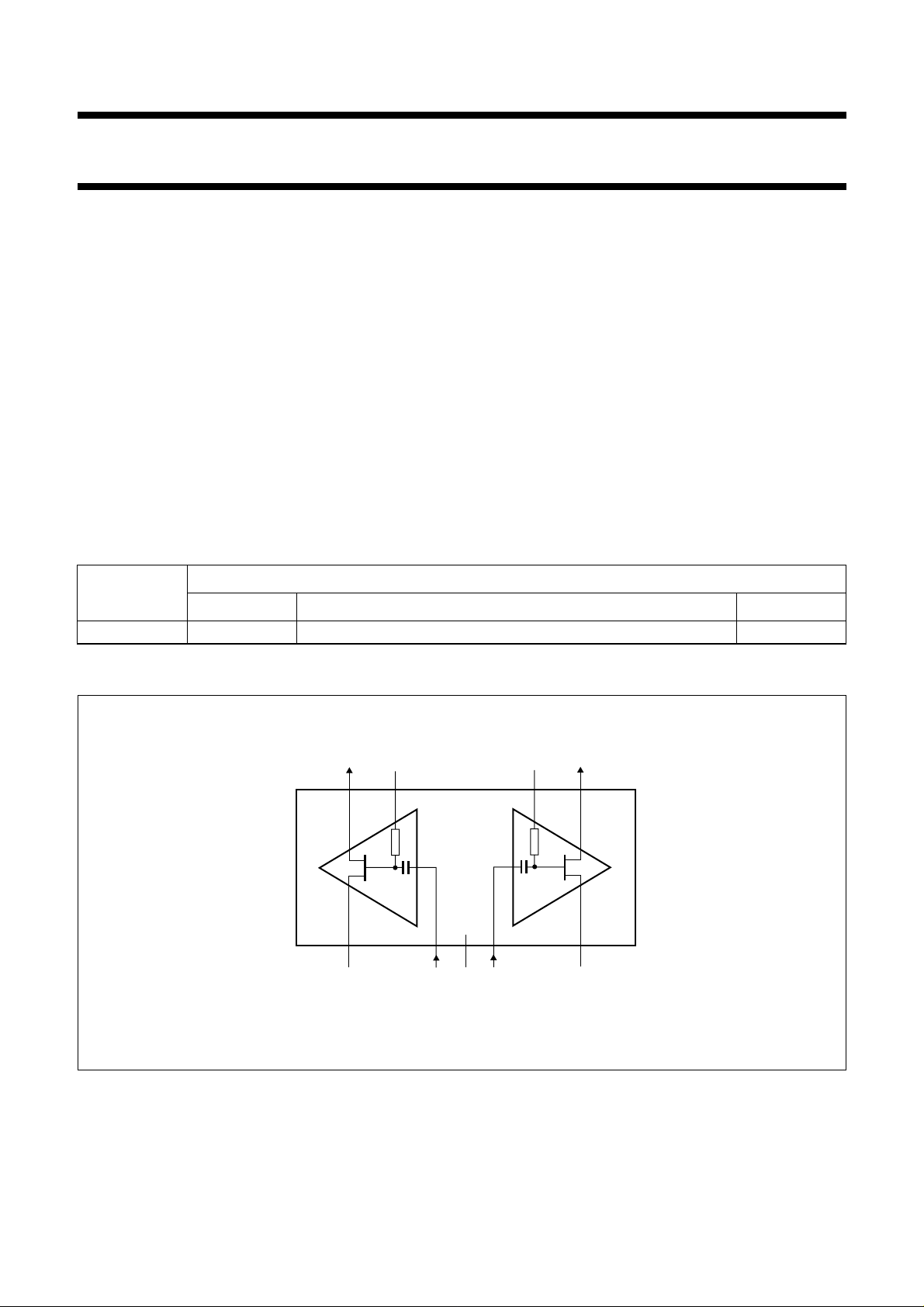
BLOCK DIAGRAM
handbook, full pagewidth
OUT2
1, 2,
14, 15
V
S2
V
G2
16
13 12 9
CGY2105ATS
n.c.
IN2 IN1
Fig.1 Block diagram.
OUT1
V
G1
7, 8,
64, 5
10, 113
FCA096
V
S1
1999 Dec 23 2
Philips Semiconductors Preliminary specification
High dynamic range dual LNA MMIC CGY2105ATS
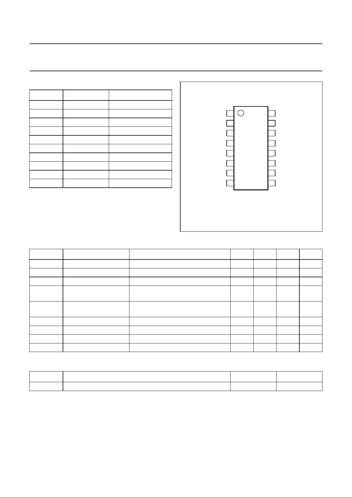
PINNING
SYMBOL PIN DESCRIPTION
V
S2
IN2 3 amplifier 2 input
n.c. 4 not connected
n.c. 5 not connected
IN1 6 amplifier 1 input
V
S1
OUT1 9 amplifier 1 drain output
V
G1
V
G2
OUT2 16 amplifier 2 drain output
1, 2, 14 and 15 amplifier 2 source
7, 8, 10 and 11 amplifier 1 source
12 amplifier 1 gate bias
13 amplifier 2 gate bias
handbook, halfpage
V
V
V
V
S2
S2
IN2
n.c.
n.c.
IN1
S1
S1
1
2
3
4
CGY2105ATS
5
6
7
8
FCA097
OUT2
16
V
15
S2
V
14
S2
V
13
G2
V
12
G1
V
11
S1
V
10
S1
OUT1
9
Fig.2 Pin configuration.
LIMITING VALUES
SYMBOL PARAMETER CONDITIONS MIN. TYP. MAX. UNIT
V
DS
V
GS
V
DG
V
supply
drain-source voltage −−5V
gate-source voltage −3 − +1 V
drain-gate voltage −−7V
positive supply voltage see Chapter “Application and test
−−6V
information”
V
neg
negative supply voltage see Chapter “Application and test
−6 −−V
information”
T
amb
T
j
T
stg
P
tot
ambient temperature −40 − +85 °C
junction temperature −−150 °C
storage temperature −−150 °C
total power dissipation T
<85°C −−430 mW
amb
THERMAL CHARACTERISTICS
SYMBOL PARAMETER VALUE UNIT
R
th(j-a)
thermal resistance from junction to ambient 138 K/W
1999 Dec 23 3
Philips Semiconductors Preliminary specification
High dynamic range dual LNA MMIC CGY2105ATS
CHARACTERISTICS
T
=25°C; measured and guaranteed only for the application shown in Chapter “Application and test information”;
amb
unless otherwise specified.
SYMBOL PARAMETER CONDITIONS MIN. TYP. MAX. UNIT
Supplies
I
supply
I
neg
Amplifiers: V
f
i
G gain f
∆G
(T)
NF noise figure − 0.55 0.8 dB
∆NF
(T)
IP3
i
∆IP3
i(T)
ISO
r
ISO
i
s
11
s
22
positive supply current (for each LNA) V
negative supply current (for each LNA) V
supply
= 5.0 V; V
= −5.0 V; Z0=50Ω; both LNAs biased; duty cycle 100%
neg
V
V
supply
neg
supply
neg
= 5.0 V;
= −5.0 V
= 5.0 V;
= −5.0 V
42 58 72 mA
− 0.3 0.4 mA
input frequency 1710 − 1910 MHz
= 1710 MHz 16 16.9 17.8 dB
i
f
= 1710 to 1910 MHz 14.8 16.3 17.8 dB
i
gain variation with temperature −40 °C<T
noise figure variation with temperature −40 °C<T
< +85 °C −±0.45 − dB
amb
< +85 °C −±0.25 − dB
amb
input third-order intercept point ∆f=±0.5 MHz 11 13.5 − dBm
input third-order intercept point
−40 °C<T
< +85 °C −±0.45 − dB
amb
variation with temperature
reverse isolation 18 20 − dB
isolation between inputs 21 23 − dB
input reflection coefficient 50 Ω source −−8.5 − dB
output reflection coefficient 50 Ω load −−22 − dB
1999 Dec 23 4
Philips Semiconductors Preliminary specification
High dynamic range dual LNA MMIC CGY2105ATS
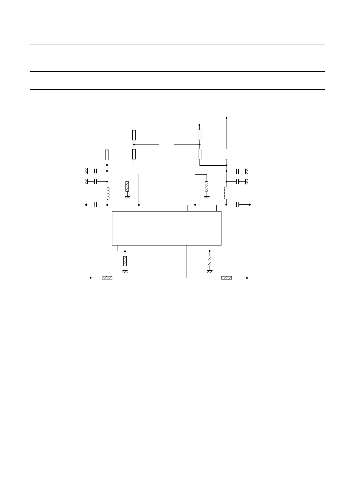
APPLICATION AND TEST INFORMATION
handbook, full pagewidth
R3
R5
TRL5
11 10 916 15
R1
C1
C3
L1
C5
OUT2
C2
C4
C6
R2
R4
R6
TRL6
L2
14 13 12
CGY2105ATS
123
TRL4
TRL2
IN2 IN1
4, 5 768
n.c.
TRL3
TRL1
V
V
OUT1
FCA098
supply
neg
The demonstration board has been optimized for a centre frequency of 1.8 GHz.
The MMIC s-parameters (typical values) in a range from 0.1 to 6 GHz are available on request.
Fig.3 Application diagram.
1999 Dec 23 5