

Philips CGY2032TS-C1 Datasheet

DATA SH EET
Product specification
Supersedes data of 1998 Nov 23
File under Integrated Circuits, IC17
1999 Jul 21
INTEGRATED CIRCUITS
CGY2032TS
DECT 500 mW power amplifier
1999 Jul 21 2
Philips Semiconductors Product specification
DECT 500 mW power amplifier CGY2032TS
FEATURES
• Power Amplifier (PA) overall efficiency 55%
• 27.5 dBm saturated output power at 3.2 V
• 0 dBm input power
• 40 dB linear gain
• Operation without negative supply
• Wide operating temperature range −30 to +85 °C
• SSOP16 package.
APPLICATIONS
• 1.88 to 1.9 GHz transceivers for DECT applications
• 2 GHz transceivers [Personal Handy phone System
(PHS), Digital Cellular System (DCS) and Personal
Communication Services (PCS)].
GENERAL DESCRIPTION
The CGY2032TS is a GaAs Monolithic Microwave
Integrated Circuit (MMIC) power amplifier specifically
designed to operate from 3.6 V battery supply.
No negative supply voltage is required for operation.
QUICK REFERENCE DATA
Note
1. For conditions, see Chapters “AC characteristics” and “DC characteristics”.
ORDERING INFORMATION
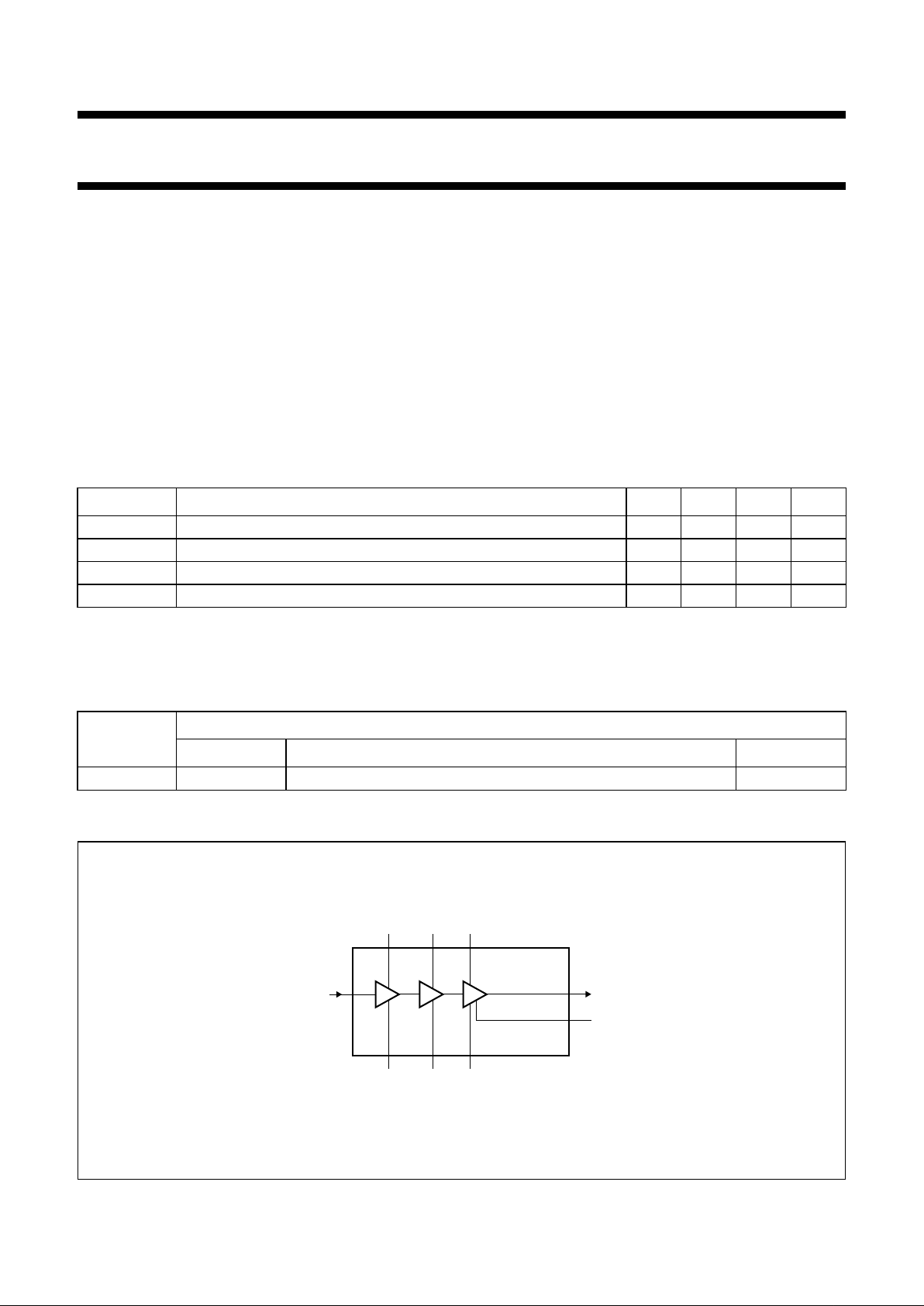
BLOCK DIAGRAM
SYMBOL PARAMETER
(1)
MIN. TYP. MAX. UNIT
V
DD
positive supply voltage − 3.2 − V
I
DD
positive peak supply current − 350 − mA
P
o
output power − 27.5 − dBm
T
amb
ambient temperature −30 − +85 °C
TYPE
NUMBER
PACKAGE
NAME DESCRIPTION VERSION
CGY2032TS SSOP16 plastic shrink small outline package; 16 leads; body width 4.4 mm SOT369-1
Fig.1 Block diagram.
handbook, halfpage
MGK735
10 6, 7
2, 3, 4
12, 13, 14
11
85
16
15
1
RFI
V
DD1
GND1 GND2 GND3
V
DD2VDD3
RFO
OPM
CGY2032TS

1999 Jul 21 3
Philips Semiconductors Product specification
DECT 500 mW power amplifier CGY2032TS
PINNING
SYMBOL PIN DESCRIPTION
V
DD3
1 third stage supply voltage
GND3 2 third stage ground supply
GND3 3 third stage ground supply
GND3 4 third stage ground supply
V
DD2
5 second stage supply voltage
GND2 6 second stage ground supply
GND2 7 second stage ground supply
V
DD1
8 first stage supply voltage
n.c. 9 not connected
GND1 10 first stage ground supply
RFI 11 PA input
GND3 12 third stage ground supply
GND3 13 third stage ground supply
GND3 14 third stage ground supply
OPM 15 output pre-matching
RFO 16 PA output
Fig.2 Pin configuration.
handbook, halfpage
CGY2032TS
MGK734
1
2
3
4
5
6
7
8
16
15
14
13
12
11
10
9
V
DD3
GND3
GND3
GND3
V
DD2
GND2
GND2
V
DD1
n.c.
GND1
RFI
GND3
GND3
GND3
OPM
RFO
FUNCTIONAL DESCRIPTION
Amplifier
The CGY2032TS is a 3-stage GaAs power amplifier
capableofdelivering500 mW(typ.)at1.9 GHzintoa 50 Ω
load. Each amplifier stage has an open-drain
configuration. The drains have to be loaded externally by
adequate reactive circuits which must also provide a DC
path to the supply.
The amplifier can be switched off by means of a single
external PNP or PMOS series switch connected between
the battery and the amplifier drains.
This switch can also be used to vary the actual supply
voltage applied to the amplifier and hence, control the
output power.
This device is specifically designed to work with a duty
factor of 50% and can work up to 100% with good thermal
performance printed-circuit boards.
Biasing
Internal biasing is provided inside the amplifier for
class AB operation.
LIMITING VALUES
In accordance with the Absolute Maximum Rating System (IEC 134).
Notes
1. On Philips evaluation board.
2. On Philips evaluation board, P
tot
maximum value is 800 mW.
SYMBOL PARAMETER CONDITIONS MIN. MAX. UNIT
V
DD
operating supply voltage note 1 − 5.2 V
T
j(max)
maximum operating junction temperature − 150 °C
P
tot
total power dissipation note 2 − 450 mW
P
i
input power − 15 dBm
T
stg
storage temperature −55 +125 °C
1999 Jul 21 4
Philips Semiconductors Product specification
DECT 500 mW power amplifier CGY2032TS
HANDLING
Do not operate or store near strong electrostatic fields. Meets class 1 ESD test requirements [Human Body Model
(HBM)], in accordance with
“MIL STD 883C - method 3015”
.
THERMAL CHARACTERISTICS
Note
1. On Philips evaluation board, R
th(j-a)
value is typically 80 K/W.
DC CHARACTERISTICS
T
amb
=25°C; unless otherwise specified.
AC CHARACTERISTICS
V
DD
= 3.2 V; fRF= 1900 MHz; Pi= 0 dBm; T
amb
=25°C; duty factor δ = 50%; 50 Ω impedance system; measured and
guaranteed on the CGY2032TS evaluation board; the circuit diagram is shown in Fig.5.
Note
1. The device is adjusted to provide nominal value of load power into a 50 Ω load. The device is switched off and a 6 : 1
load replaces the 50 Ω load. The device is switched on and the phase of the 6 : 1 load is varied
360 electrical degrees during a 60 seconds test period.
SYMBOL PARAMETER CONDITIONS VALUE UNIT
R
th(j-a)
thermal resistance from junction to ambient in free air; note 1 145 K/W
SYMBOL PARAMETER CONDITIONS MIN. TYP. MAX. UNIT
Pins V
DD1,VDD2
and V
DD3
V
DD
positive supply voltage 1.8 3.2 4.2 V
I
DD
positive peak supply current VDD= 3.2 V −−800 mA
SYMBOL PARAMETER CONDITIONS MIN. TYP. MAX. UNIT
P
i
input power −5 0 +5 dBm
δ duty factor − 50 100 %
P
o
output power 26.5 27.5 29 dBm
I
DD
total drain current −−500 mA
η efficiency − 55 − %
P
leak
RF leakage to output in power off state VDD=0V −−40 −35 dBm
H2 second harmonic level −−−30 dBc
H3 third harmonic level −−−35 dBc
Stab stability (spurious levels) note 1 −−60 − dBc
 Loading...