

Philips CGY2014ATW Datasheet
INTEGRATED CIRCUITS
DATA SH EET
CGY2014ATW
GSM/DCS/PCS power amplifier
Preliminary specification
File under Integrated Circuits, IC17
2000 Nov 28
Philips Semiconductors Preliminary specification
GSM/DCS/PCS power amplifier CGY2014ATW
FEATURES
• Operates at 3.6 V battery supply voltage
• Power Amplifier (PA) output power:
35 dBm in GSM band and 32.5 dBm in DCS/PCS band
• Input power: 5 dBm in GSM band and DCS/PCS band
• Wide operating temperature range from
T
= −20 to +85 °C
amb
GENERAL DESCRIPTION
The CGY2014ATW is a dual-band GSM/DCS/PCS GaAs
Monolithic Microwave Integrated Circuit (MMIC) power
amplifier. The circuit is specifically designed to operate at
3.6 V battery supply voltage.
The power amplifier requires only a 30 dB harmonic
low-pass filter to comply with the transmit spurious
specification.
• HTSSOP20 exposed die pad package.
The voltages applied on pinsVDD(drain) control the power
of the power amplifier and enable it to be switched off.
APPLICATIONS
• Dual-band systems: Low Band (LB) from
880 to 915 MHz hand-held transceiversfor E-GSM and
High Band (HB) from 1710 to 1910 MHz for DCS/PCS
applications.
QUICK REFERENCE DATA
SYMBOL PARAMETER MIN. TYP. MAX. UNIT
V
DD
I
DD(LB)
P
o(LB)(max)
I
DD(HB)
P
o(HB)(max)
T
amb
supply voltage − 3.5 5.2 V
GSM positive peak supply current − 2 − A
maximum output power in GSM band 34.5 35 − dBm
DCS/PCS positive peak supply current − 1.5 − A
maximum output power in DCS/PCS band 32 32.5 − dBm
ambient temperature −20 − +85 °C
ORDERING INFORMATION
TYPE
NUMBER
NAME DESCRIPTION VERSION
PACKAGE
CGY2014ATW HTSSOP20 plastic, heatsink thin shrink small outline package; 20 leads;
body width 4.4 mm
2000 Nov 28 2
SOT527-1

Philips Semiconductors Preliminary specification
GSM/DCS/PCS power amplifier CGY2014ATW
BLOCK DIAGRAM
handbook, full pagewidth
RFI(LB)
n.c.
GND
RFI(HB)
GND1(LB)
8
9
1, 10, 12,
16, 19
15
2
V
DD1(LB)
V
DD2(LB)
7
6
CGY2014ATW
3 4, 5
V
DD1(HB)
V
DD2(HB)
Fig.1 Block diagram.
13, 14
17, 18
RFO/V
DD3(LB)
11
V
GLB
20
V
GHB
RFO/V
DD3(HB)
FCA196
2000 Nov 28 3
Philips Semiconductors Preliminary specification
GSM/DCS/PCS power amplifier CGY2014ATW
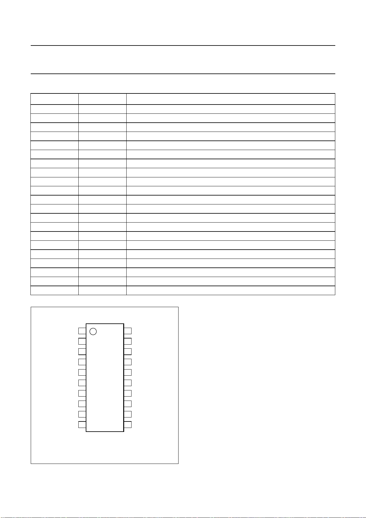
PINNING
SYMBOL PIN DESCRIPTION
n.c. 1 not connected
RFI(HB) 2 DCS/PCS power amplifier input
V
DD1(HB)
V
DD2(HB)
V
DD2(HB)
V
DD2(LB)
V
DD1(LB)
GND1(LB) 8 GSM first stage ground
RFI(LB) 9 GSM power amplifier input
n.c. 10 not connected
V
GLB
n.c. 12 not connected
RFO/V
DD3(LB)
RFO/V
DD3(LB)
GND 15 ground
n.c. 16 internal connection to ground; pin should not be connected to the board
RFO/V
DD3(HB)
RFO/V
DD3(HB)
n.c. 19 not connected
V
GHB
− exposed die ground
3 DCS/PCS first stage supply voltage
4 DCS/PCS second stage supply voltage
5 DCS/PCS second stage supply voltage
6 GSM second stage supply voltage
7 GSM first stage supply voltage
11 GSM power amplifier gates
13 GSM power amplifier output and third stage supply voltage
14 GSM power amplifier output and third stage supply voltage
17 DCS/PCS power amplifier output and third stage supply voltage
18 DCS/PCS power amplifier output and third stage supply voltage
20 DCS/PCS power amplifier gates
handbook, halfpage
V
DD1(HB)
V
DD2(HB)
V
DD2(HB)
V
DD2(LB)
V
DD1(LB)
GND1(LB)
n.c.
RFI(HB)
RFI(LB)
n.c.
1
2
3
4
5
CGY2014ATW
6
7
8
9
10
FCA197
20
19
18
17
16
15
14
13
12
11
V
GHB
n.c.
RFO/V
RFO/V
n.c.
GND
RFO/V
RFO/V
n.c.
V
GLB
DD3(HB)
DD3(HB)
DD3(LB)
DD3(LB)
Fig.2 Pin configuration.
2000 Nov 28 4
FUNCTIONAL DESCRIPTION
Operating conditions
The CGY2014ATW is designed to meet the European
Telecommunications Standards Institute (ETSI) GSM
documents, the
“ETS 300 577 specification”
, which are
defined as follows:
• ton= 570 µs
• T = 4.16 ms
• Duty cycle δ =1/8.
Multislot operation can be implemented provided that the
application circuit does not drive the IC beyond the limiting
values.
Power amplifier
The GSM and DCS/PCS power amplifiers consist of three
cascaded gain stages with an open-drain configuration.
Each drain has to be loaded externally by an adequate
reactive circuit which also has to be a DC path to the
supply.
 Loading...