

Page 1

Bluetooth Car entertainment system
CEM5000/00/55/51
CEM5000X/78
CONTENTS
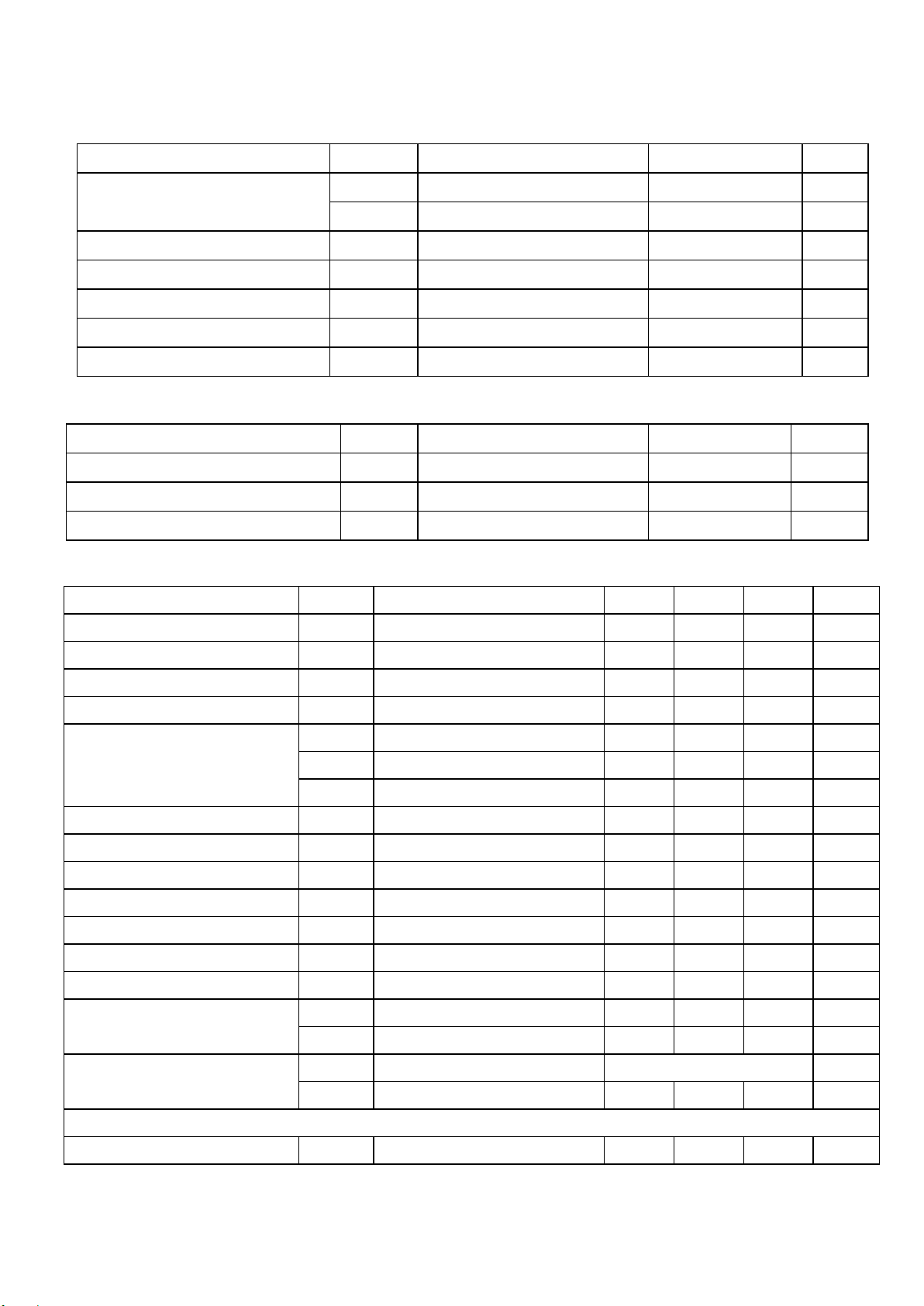
Technical specification ..................................................................1-2
Service measurement setup..........................................................1-3
Service aids .................................................................................1-4
Instructions on CD playability ...............................................2-1.. 2-2
Block diagram ................................................................................3-1
Wiring diagram ..............................................................................4-1
Main board
Circuit diagram ..................................................................5-1..5-5
Layout diagram..................................................................5-6..5-7
Panel board
Circuit diagram .........................................................................6-1
Layout diagram..................................................................6-2..6-3
Servo board
Circuit diagram...................................................................7-1..7-2
Layout diagram .........................................................................7-3
Exploded view diagram .................................................................8-1
Revision list ...................................................................................9-1
©
Copyright 2010 Philips Consumer Electronics B.V. Eindhoven, The Netherlands
All rights reserved. No part of this publication may be reproduced, stored in a retrieval
system or transmitted, in any form or by any means, electronic, mechanical, photocopying,
or otherwise without the prior permission of Philips.
Published by LX 1036 Service Audio Subject to modification
Version 1.1
3141 785 35011
Page 2
TECHNICAL SPECIFICATION
1 - 2
Radio
Power supply 12 V DC (10.8 V
- 15.8 V), nega ve
ground
Fuse 15 A
Suitable speaker
4 - 8
impedance
Maximum power
50 W x 4 channels
output
Con nuous power
output
Pre-Amp output
voltage
24 W x 4 channels
10% T.H.D.)
(4
2.0 V ( USB play
mode; 1 kHz, 0 dB, 10
k load)
Subwoofer output
voltage
Aux-in level
Dimensions ( W x H
2.0 V (USB play
mode: 61 Hz, 0 dB, 10
load)
k
500 mV
188 x 58 x 212 mm
x D)
Weight 1.67 kg
Opera on
-20°c -- 70°c
temperature
Frequency
range - FM
87.5 - 108.0 MHz (Europe)
87.5 - 107.9 MHz
(American)
Frequency
range -
522 - 1620 KHz (Europe)
530 - 1710 HKz (American)
AM(MW)
Usable
8 V
sensi vity - FM
Usable
30 V
sensi vity AM(MW)
Bluetooth
Output power 0 dBm (Class 2)
Frequency band 2.4000 GHz - 2.4835 GHz
ISM Band
Range 3 meters(free space)
Standard Bluetooth 2.0 speci? ca on
VERSION VARIATION
Type /Versions:
Board in used:
SERVO BOARD
MAIN BOARD
PANEL BOARD
Features
RDS
VOLTAGE SELECTOR
ECO STANDBY - DARK
* TIPS : C -- Component Lever Repair.
M -- Module Lever Repair
-- Used
Service policy
Type /Versions:
Feature diffrence
/05 /00
C/M
C/M
C/M
/05 /00
CEM5000
/55
C/M
C/M
C/M
CEM5000
/55
89/15/85/
C/M
C/M
C/M
89/15/85/
Page 3
e
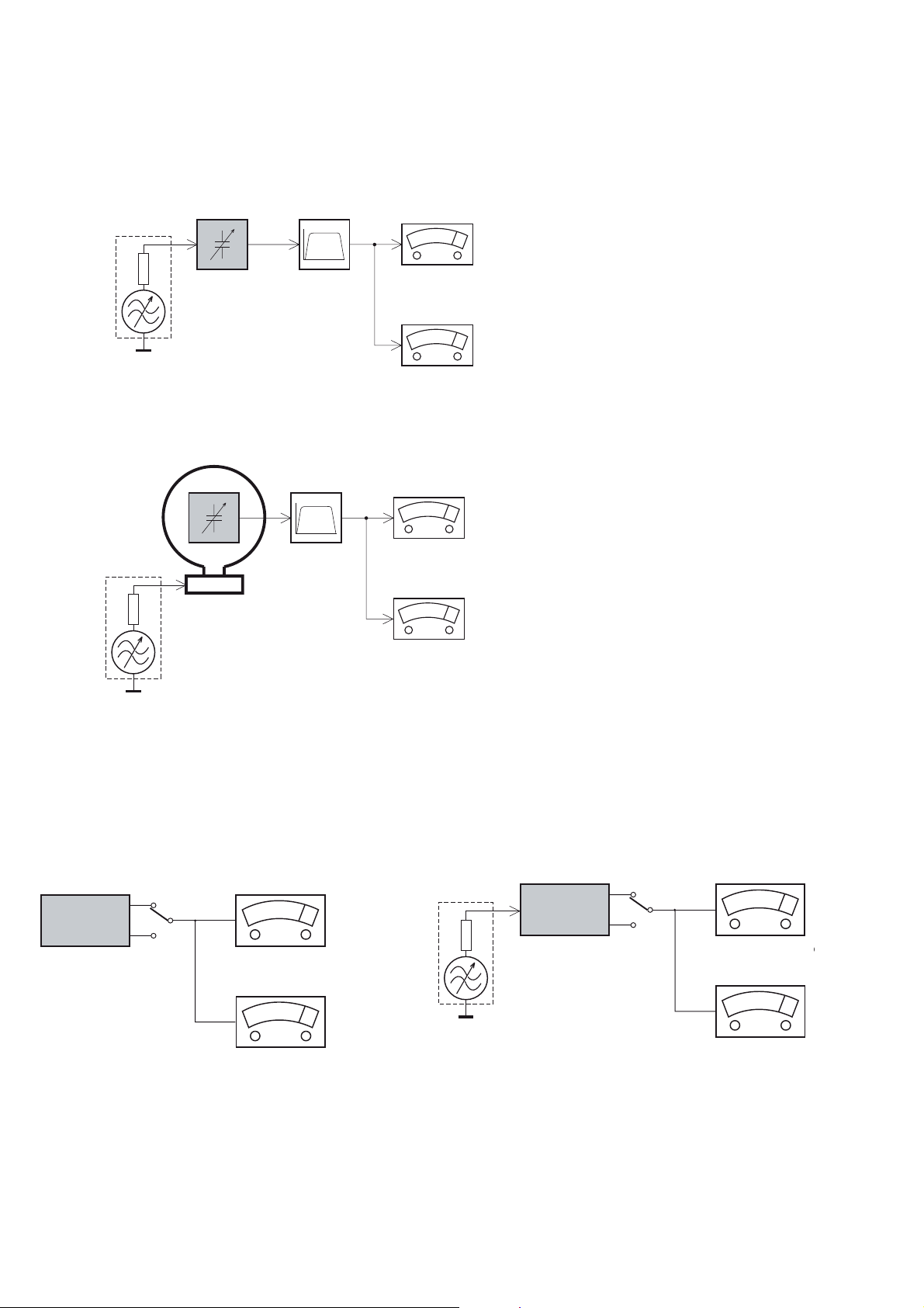
MEASUREMENT SETUP
Tuner FM
1-3
Bandpass
LF Voltmeter
e.g. PM2534
RF Generator
e.g. PM5326
DUT
250Hz-15kHz
e.g. 7122 707 48001
Ri=50:
S/N and distortion meter
e.g. Sound Technology ST1700B
Use a bandpass filter to eliminate hum (50Hz, 100Hz) and disturbance from the pilottone (19kHz, 38kHz).
Tuner AM (MW,LW)
RF Generator
e.g. PM5326
Ri=50:
DUT
Frame aerial
e.g. 7122 707 89001
Bandpass
250Hz-15kHz
e.g. 7122 707 48001
LF Voltmeter
e.g. PM2534
S/N and distortion meter
e.g. Sound Technology ST1700B
To avoid atmospheric interference all AM-measurements have to be carried out in a Faraday´s cage.
Use a bandpass filter (or at least a high pass filter with 250Hz) to eliminate hum (50Hz, 100Hz).
CD
Use Audio Signal Disc
(replaces test disc 3)
DUT
L
R
SBC429 4822 397 30184
S/N and distortion meter
e.g. Sound Technology ST1700B
LEVEL METER
e.g. Sennheiser UPM550
-
Recorder
Use Universal Test Cassette CrO2 SBC419 4822 397 30069
or Universal Test Cassette
LF Generator
e.g. PM5110
Fe SBC420 4822 397 30071
DUT
L
R
S/N and distortion met
e.g. Sound Technology ST170
LEVEL METER
e.g. Sennheiser UPM550
with FF-filter
Page 4
SERVICE AIDS
1-4
GB
All ICs and many other semi-conductors are
susceptible to electrostatic discharges (ESD).
Careless handling during repair can reduce life
drastically.
When repairing, make sure that you are
connected with the same potential as the mass
of the set via a wrist wrap with resistance.
Keep components and tools also at this
potential.
WARNING
GB
Safety regulations require that the set be restored to its original
condition and that parts which are identical with those specified,
be used
Safety components are marked by the symbol
!
.
ESD
CLASS 1
LASER PRODUCT
Lead free
Page 5
INSTRUCTIONS ON CD PLAYABILITY
Customer complaint
"CD related problem"
Set remains closed!
check playability
1
2 - 1
playability
ok ?
Y
Play a CD
for at least 10 minutes
check playability
playability
ok ?
Y
N
"fast" lens cleaning
check playability
playability
ok ?
N
3
N
Y
For flap loaders (= access to CD drive possible)
cleaning method
4 is recommended
add Info for customer
"SET OK"
2
return set
1 - 4 For description - see following pages
Exchange CDM
Page 6
INSTRUCTIONS ON CD PLAYABILITY
2 - 2
1
PLAYABILITY CHECK
For sets which are compatible with CD-RW discs
use CD-RW Printed Audio Disc....................7104 099 96611
TR 3 (Fingerprint)
TR 8 (600µ Black dot) maximum at 01:00
• playback of these two tracks without audible disturbance
playing time for: Fingerprint
Black dot from 00:50 to 01:10
• jump forward/backward (search) within a reasonable time
For all other sets
use CD-DA SBC 444A..................................4822 397 30245
TR 14 (600µ Black dot) maximum at 01:15
TR 19 (Fingerprint)
TR 10 (1000µ wedge)
• playback of all these tracks without audible disturbance
playing time for: 1000µ wedge 10seconds
Fingerprint 10seconds
Black dot from 01:05 to 01:25
• jump forward/backward (search) within a reasonable time
10seconds
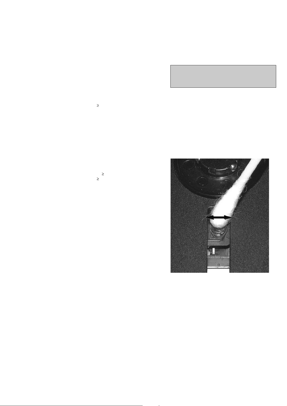
4
LIQUID LENS CLEANING
Before touching the lens it is advised to clean the
surface of the lens by blowing clean air over it.
This to avoid that little particles make scratches on
the lens.
Because the material of the lens is synthetic and coated
with a special anti-reflectivity layer, cleaning must be done
with a non-aggressive cleaning fluid. It is advised to use
“Cleaning Solvent
The actuator is a very precise mechanical component and
may not be damaged in order to guarantee its full function.
Clean the lens gently (don’t press too hard) with a soft and
clean cotton bud moistened with the special lens cleaner.
The direction of cleaning must be in the way as indicated in
the picture below.
2
CUSTOMER INFORMATION
It is proposed to add an addendum sheet to the set which
informs the customer that the set has been checked
carefully - but no fault was found.
The problem was obviously caused by a scratched, dirty or
copy-protected CD. In case problems remain, the customer
is requested to contact the workshop directly.
The lens cleaning (method 3) should be mentioned in the
addendum sheet.
The final wording in national language as well as the printing
is under responsibility of the Regional Service Organizations.
Page 7
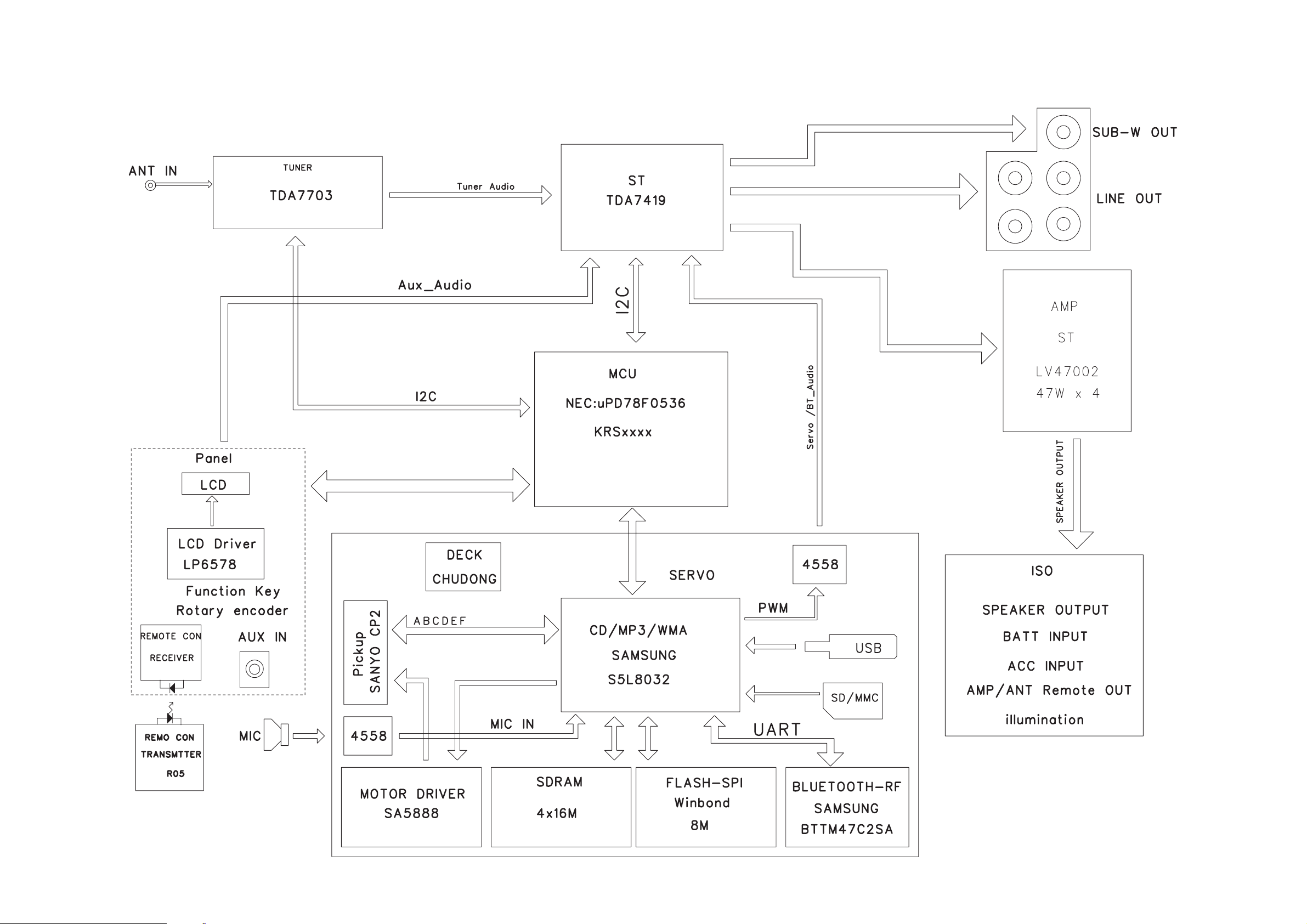
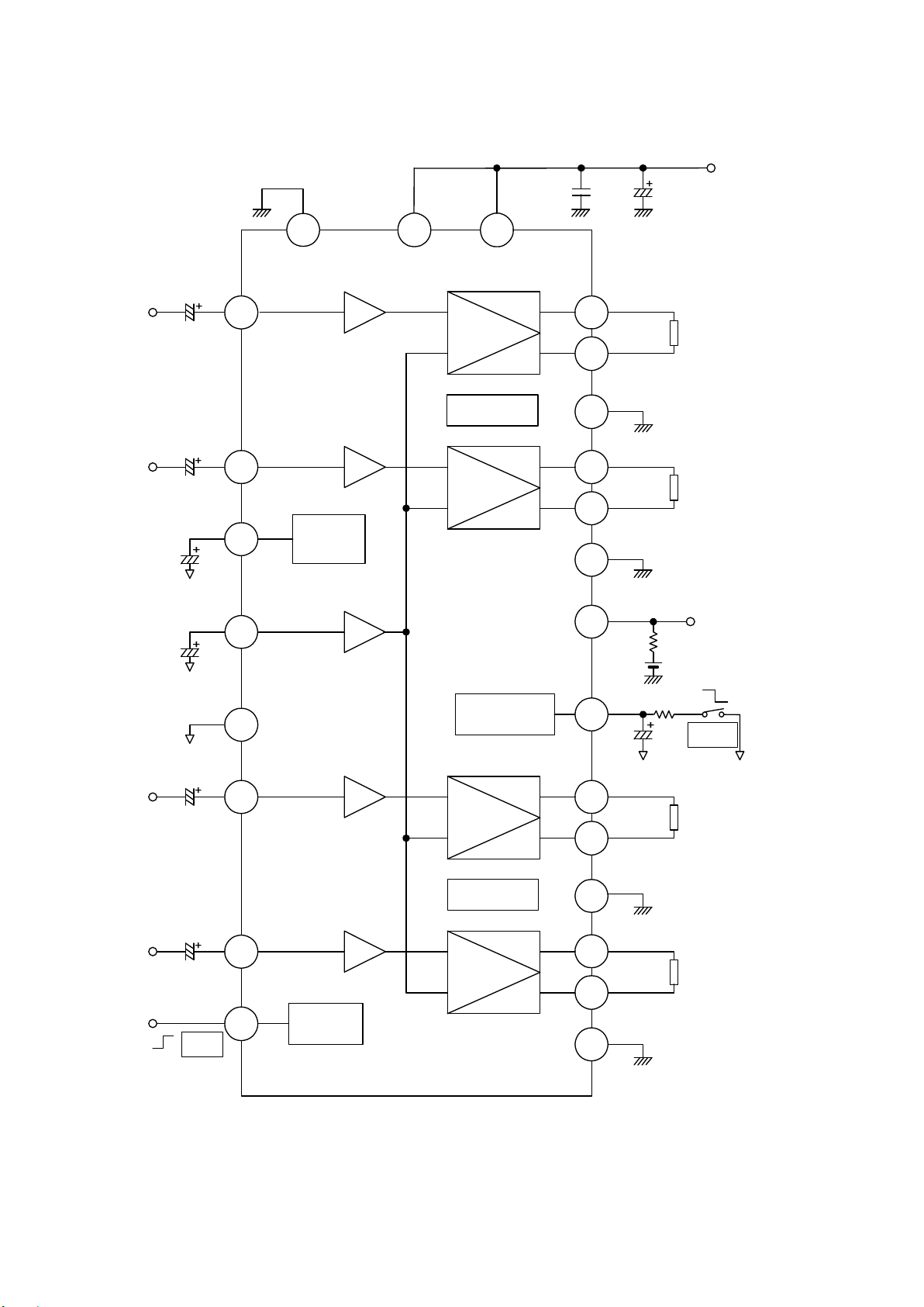
SET BLOCK DIAGRAM
3 - 1
3 - 1
Page 8
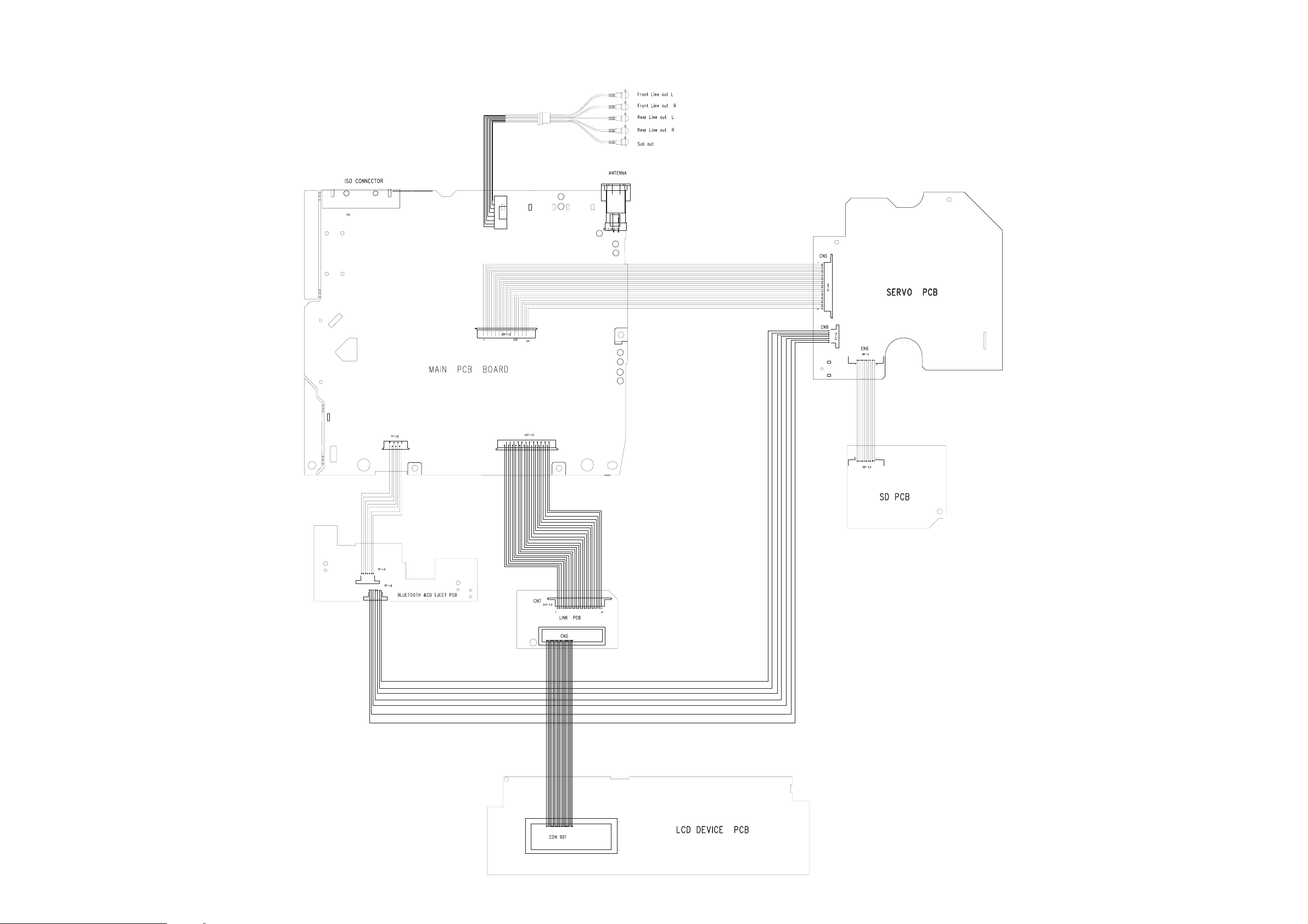
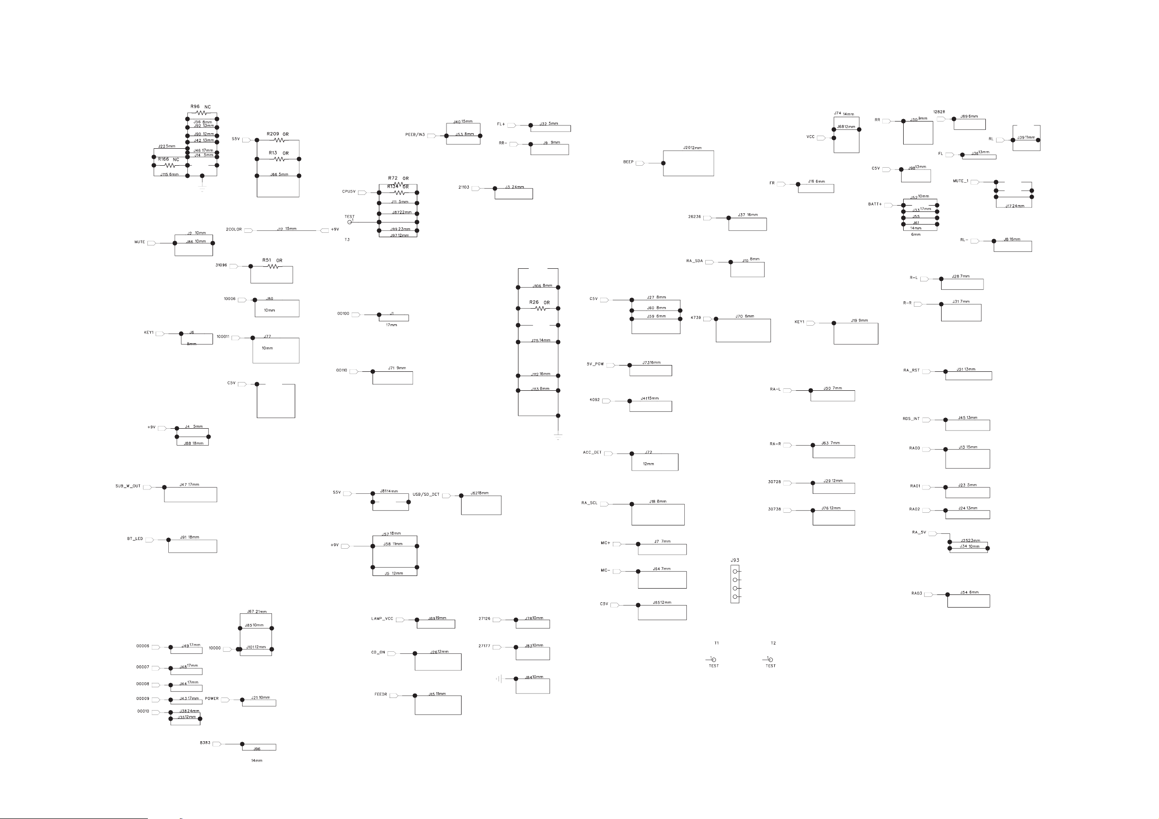
SET WIRING DIAGRAM
4 - 1 4- 1
Page 9
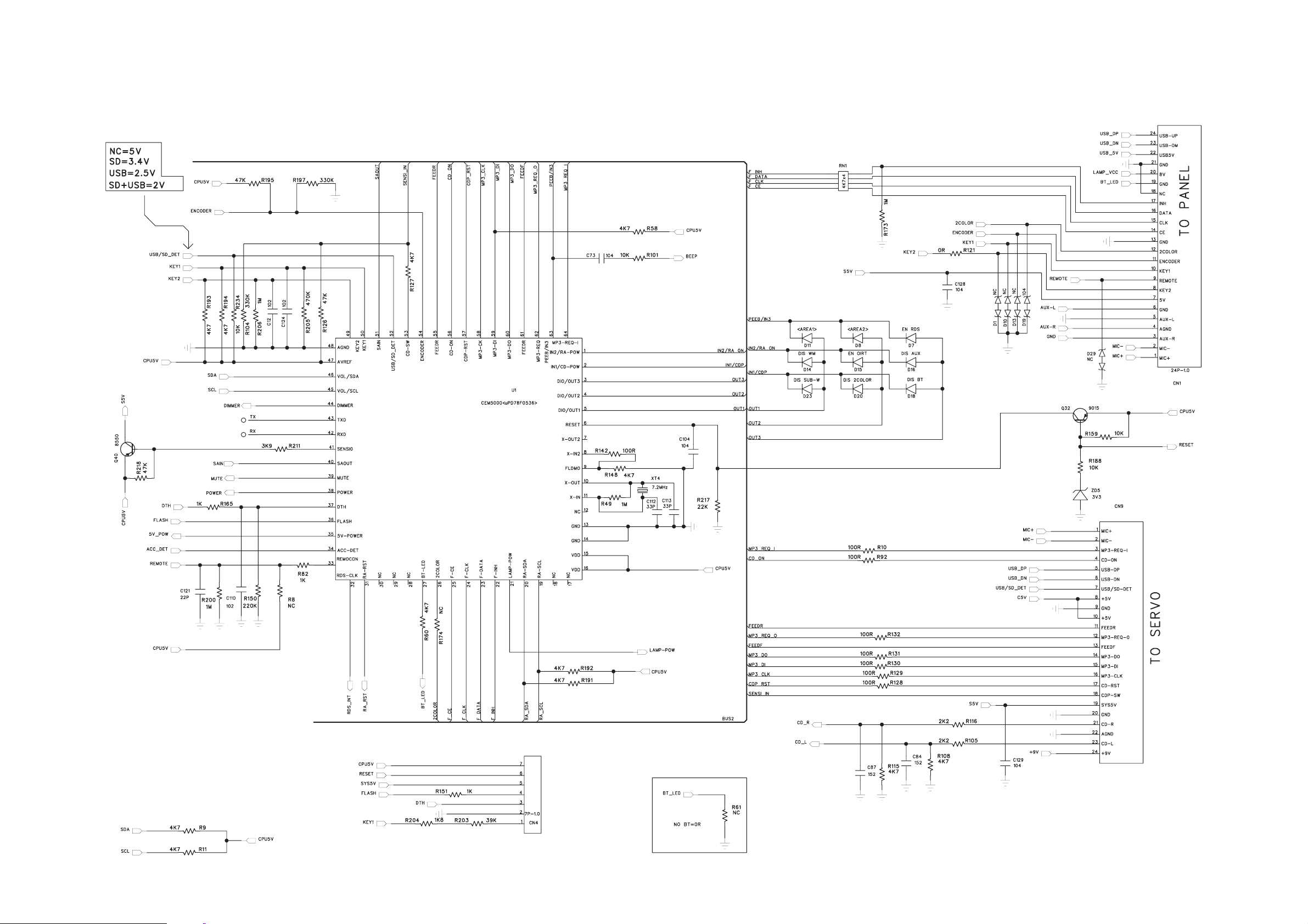
CIRCUIT DIAGRAM - MAIN BOARD
PART 1
5 - 15 - 1
Page 10
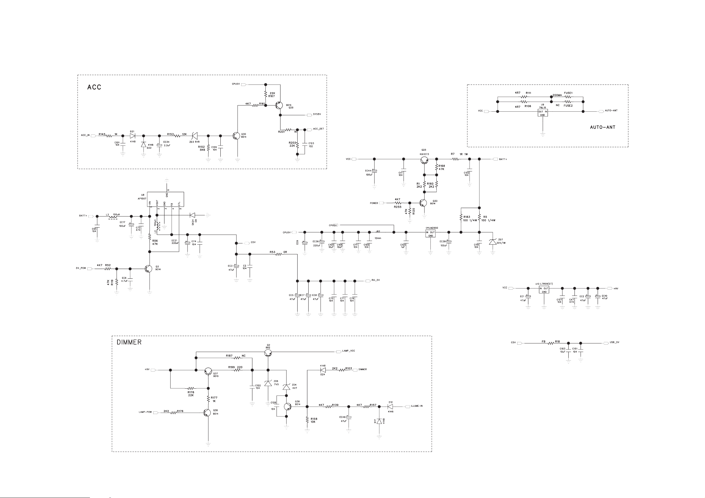
CIRCUIT DIAGRAM - MAIN BOARD
PART 2
5 - 2
5 - 2
Page 11
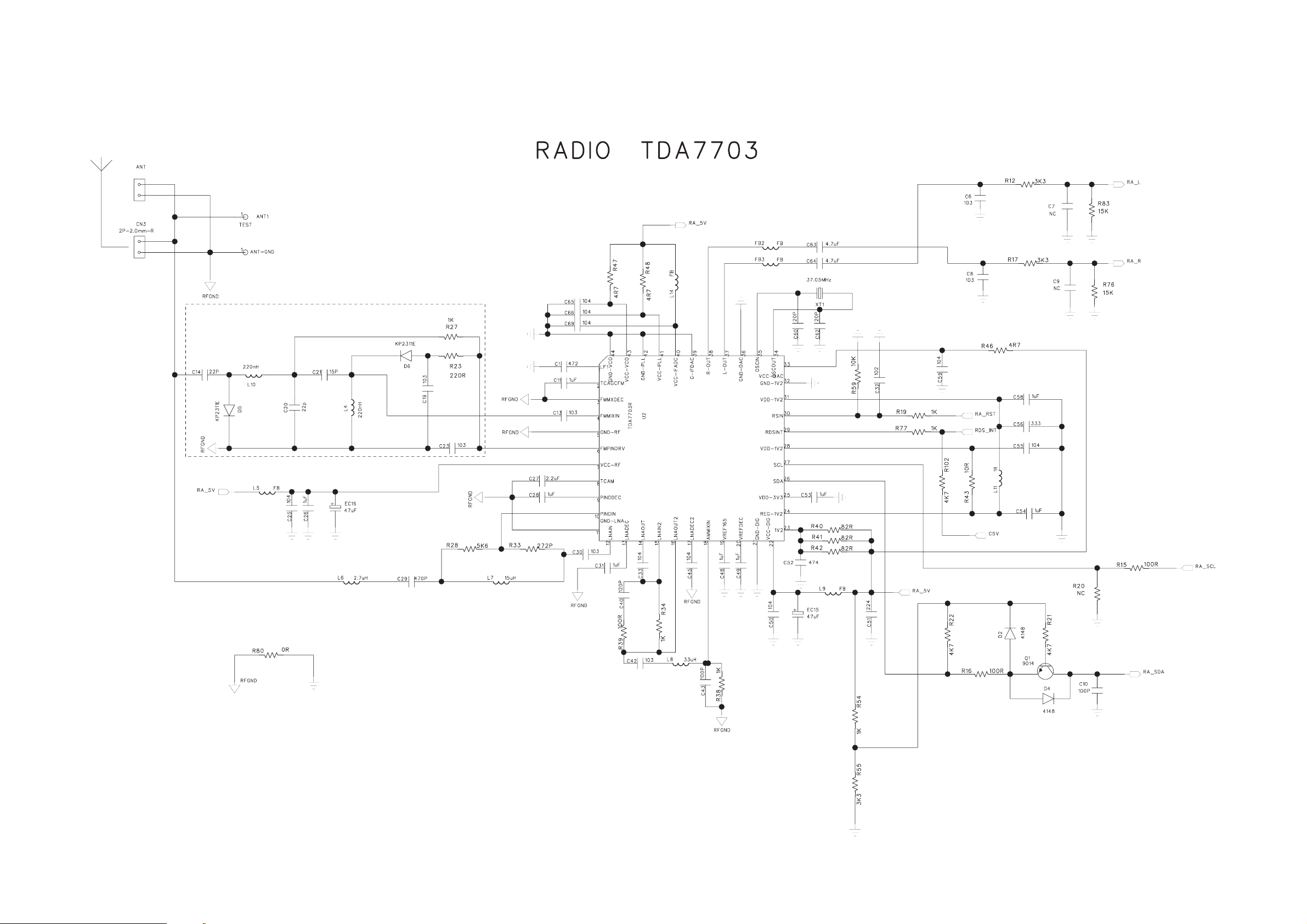
CIRCUIT DIAGRAM - MAIN BOARD
PART 3
5 - 3
5 - 3
Page 12
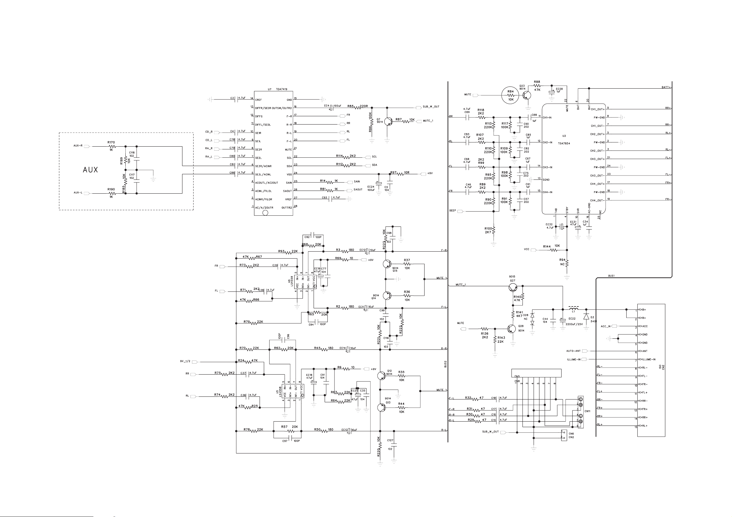
CIRCUIT DIAGRAM - MAIN BOARD
PART 4
5 - 4 5 - 4
Page 13
CIRCUIT DIAGRAM - MAIN BOARD
PART 5
5 - 5 5 - 5
Page 14
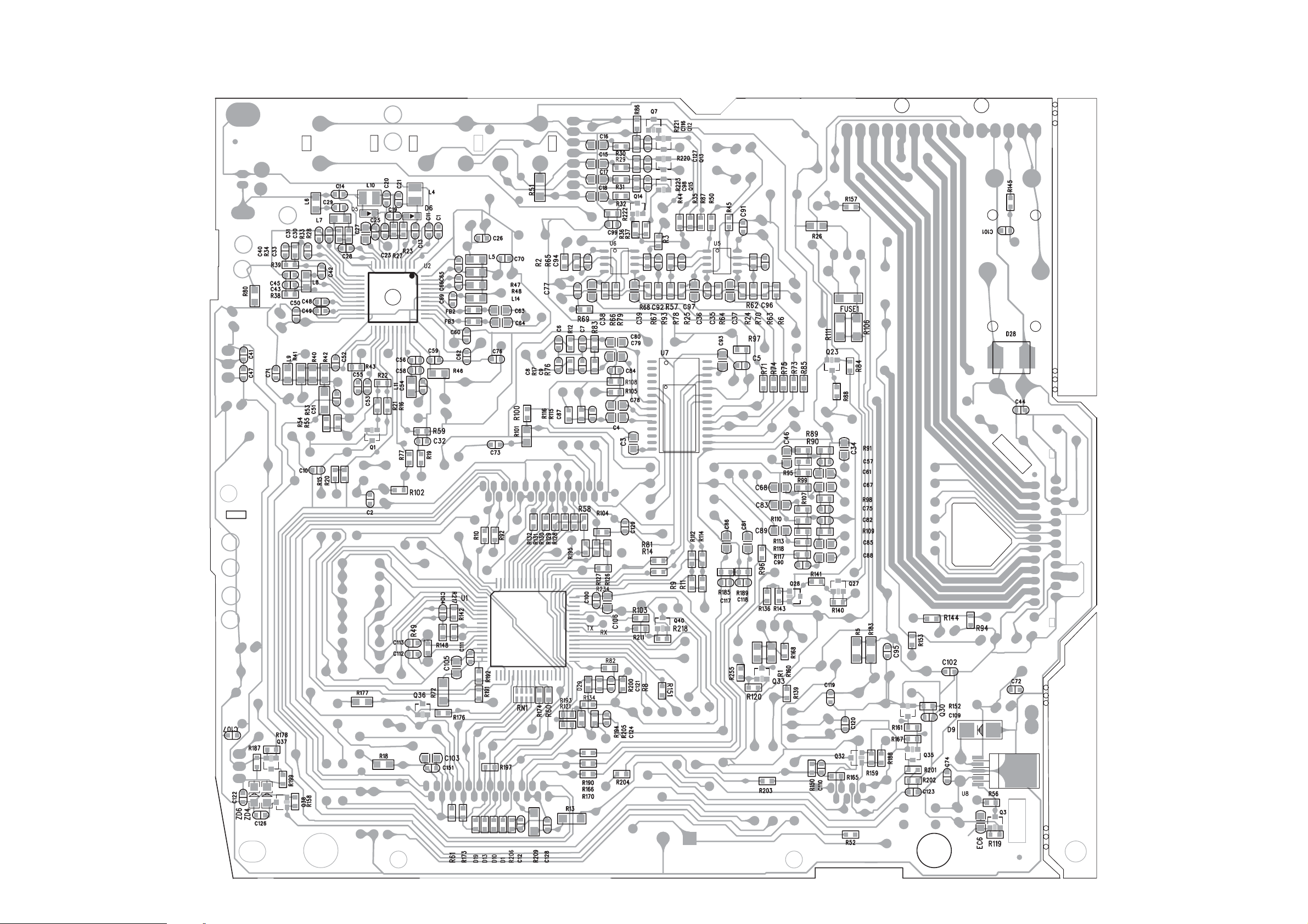
LAYOUT DIAGARM - MAIN BOARD
TOP SIDE VIEW
5 - 6
5 - 6
Page 15
LAYOUT DIAGARM - MAIN BOARD
BOTTOM SIDE VIEW
5 - 7
5 - 7
Page 16
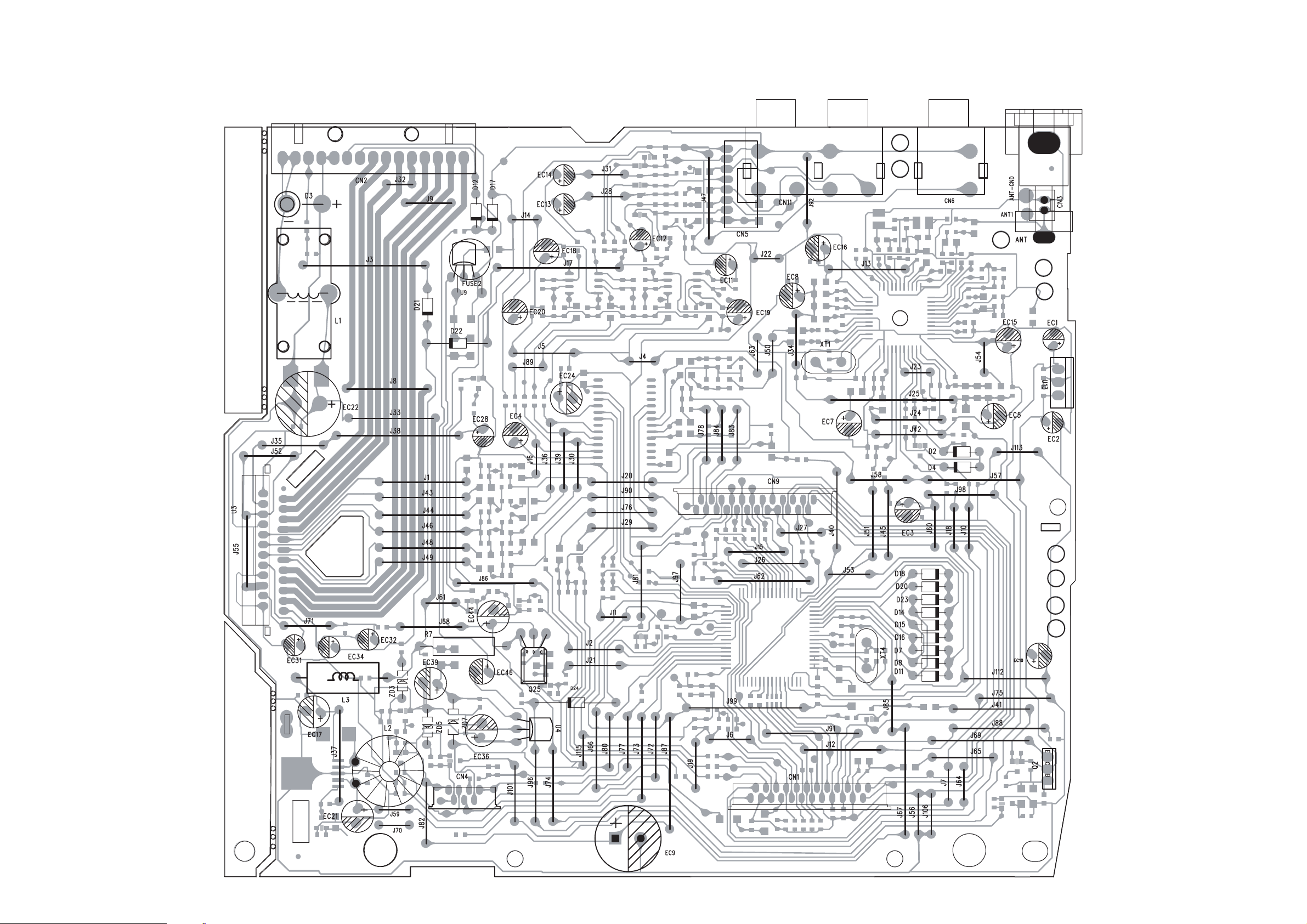
CIRCUIT DIAGARM - PANEL BOARD
6 - 1 6 - 1
CON901
24PIN
USB_UP
USB_DN
USB+5V
USB_GND
+8V
BT_LED
GND
INH
DATA
CLK
CE
GND
LCD+8V
ENCODER
KEY1
REMOTE
KEY2
+5V
AUX-L
GND
AUX-R
AGND
USB_DN
USB_UP
22K
R935
R963
NC
NC
1K
R966
R964
1K
R937
Q903
9014C
Q902
BLUE+8V
2SD1132
2SD1132
Q901
22K
R965
R938
1K
1K
R934
1K
R939
9014C
Q904
10K
R936
9014C
Q905
24
23
22
21
20
19
18
17
16
15
14
13
12
11
10
9
8
7
6
5
4
3
2
1
RED+8V
BLUE+8V
RED+8V
270
R940
LED15
R+B
RED+8V
BLUE+8V
270
470
R975
R976
LED16
R+B
470
R950
LED34
LED Q907
470
R941
270
R955
LED30
LED
270
R942
LED4
R+B
LED3
R+B
270
R959
470
R954
100
R962
470
R943
270
R960
270
R944
270
R956
LED31
LED
R933
R932
R931
R930
LED33
LED6
R+B
LED5
R+B
R929
10
LED
270
470
R945
R946
470
270
R969
R957
LED8
R+B
270
R961
LED32
LED
22
22
22
22
EC901
10uF
LED7
R+B
107
SW4
M4
R981
6V8
ZD904
12K
12K
R999
C904
680p
R904
470
108
S1S2S3S4S5S6S7S8S9
470
470
270
R948
LED9
R947
R949
R+B
470
270
470
R970
R971
R972
LED10
R+B
9013C
1
2
3
REMOTE
IC902
270
R967
LED12
R+B
270
470
R953
R952
LED13
R+B
470
270
470
R973
R974
R968
LED14
R+B
3K3
R901A
R995
270
270
R987
R+B
R+B
470
R988
470
R996
LED1
LED11
270
R993
R+B
LED2
470
R994
270
R991
R+B
270
470
R992
R989
LED17
R+B
L2
FB
4K7
R997
SW1
PAUS E SCAN
270
470
470
R985
R990
R986
LED18
LED19
R+B
C903
C906
104
C902
2P
6V8
ZD901
C905
R901
180
M1
C901
104
104
104
R983
5K6
6V8
C9102PC9122PC911
ZD902
R902
220
SW2
M2
SW3
M3
REPEAT SHUFFLE
R903
330
12K
R982
L1
FB
6V8
2P
ZD903
100
101
103
105
106
S20
S21
S22
S23
S24
S25
P3
VDD
VLCD
VLCD0
VLCD1
VLCD2
VLCD3
VLCD4
VSS
OSC
INH
CE
CLK
DI
S80
S79
R907
1K5
789
S78
S77
S26
S74
S73
S75
1
2
S1
S2
10
S76
S82
S83
SW8
TUNE/SEEK -UP
SW5
S10
S11
S12
S13
S14
S15
S16
S17
S18
S19
S11
R906
1K
12K
1
23456
S76
S83
76
77
78
79
80
81
82
83
84
85
86
87
88
89
90
91
92
93
94
95
96
97
98
99
100
S82
SW7
SUB-W
S81
S76
S77
S78
S79
S80
S81
S82
S83
S[1:120]
12K
R958
R980
R905
680
M5
SW6
M6
8788899091
9293949596
979899
102
104
LCD-59P1
LCD-59P
7273747576
7778798081
8283848586
S29
S30
S31
S32
S33
S34
S35
S66
S67
S68
6667686970
8
9
1011121314
S8
S9
S10
16
17
18
S66
S76
S77
TUNE/SEEK -D N
S64
S63
S65
IC901
PT6578LQ
S11
S12
19
20
S67
S68
SW9
S36
S62
S13
S14
LCD-49P1
LCD-49P
21
22
S69
S70
R909
3K3
S11
S28
S27
S69
S71
S70
S72
7172737475
6
7
345
S3
S4
S5S6S7
11
12
14
15
13
S79
S80
S81
S78
R908
2K2
TRACK- UP TRACK- DN
6768697071
S37
S38
S39
S40
S59
S61
S58
S60
6162636465
1516171819
S15
S16
S17
26
24
25
23
S72
S71
S73
S74
AUDIO/EQ
S41
S57
S18
S19
27
S75
SW10
S20
S21
S42
S54
S56
S55
5657585960
2021222324
S20
S21
S22
29
30
28
S47
S46
S48
R910
4K7
6263646566
S22
S52
S53
S23
313233
S49
R911
8K2
50515253545556
S68
S69
S70
S71
S72
S73
S74
PT6578LQ
414243
S58
S59
SW12
S50
S49
S48
S47
S46
S45
S44
S43
S42
S41
S40
S39
S38
S37
S36
S35
S34
S33
S32
S31
S30
S29
S28
S27
S26
464748
44
45
49
S61
S67
S60
S65
S62
S63
S64
S[1:120]
R912
18K
SW13
NC
NC
50
49
48
47
46
45
44
43
42
41
40
39
38
37
36
35
34
33
32
31
30
29
28
27
26
39
40
S56
S55
S54
S57
5758596061
S45
S44
S43
S23
S24
S51
5152535455
25
S24
S25
363738
34
35
S66
S51
S50
S52
S53
SW11
NC
123
USB
USBIN
ZR902
22P
4
ZR901
22P
R979
1K
9014C
Q906
47K
R927
VOL1
VOL
82K
R928
R924
180
SW25
MENU
R923
R918
1K5
SW20
MODE
SW23
CALL
R921
SW21
INFO
R919
1K
R920
470
680
SW22
END-CALL
R922
SW24
POWER
330
220
SW19
NC
R917
2K2
SW18
Back
R916
3K3
R915
4K7
SW17
Browser
SW16
UP
R914
8K2
SW15
DN
R913
18K
SW14
EJECT
AUX-JACK
AUX1
Page 17
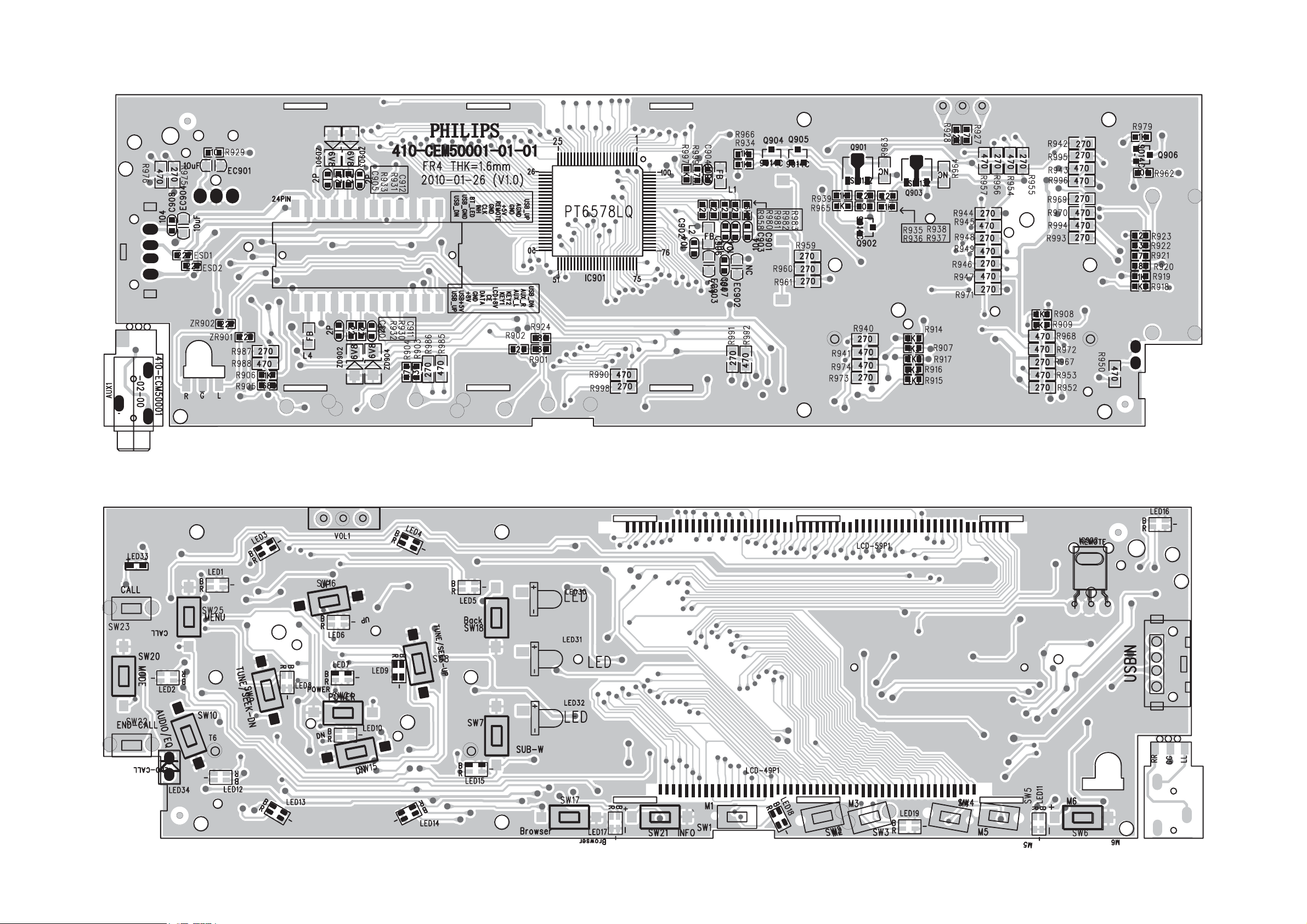
LAYOUT DIAGRAM - PANEL BOARD
6 - 2
6 - 2
Page 18
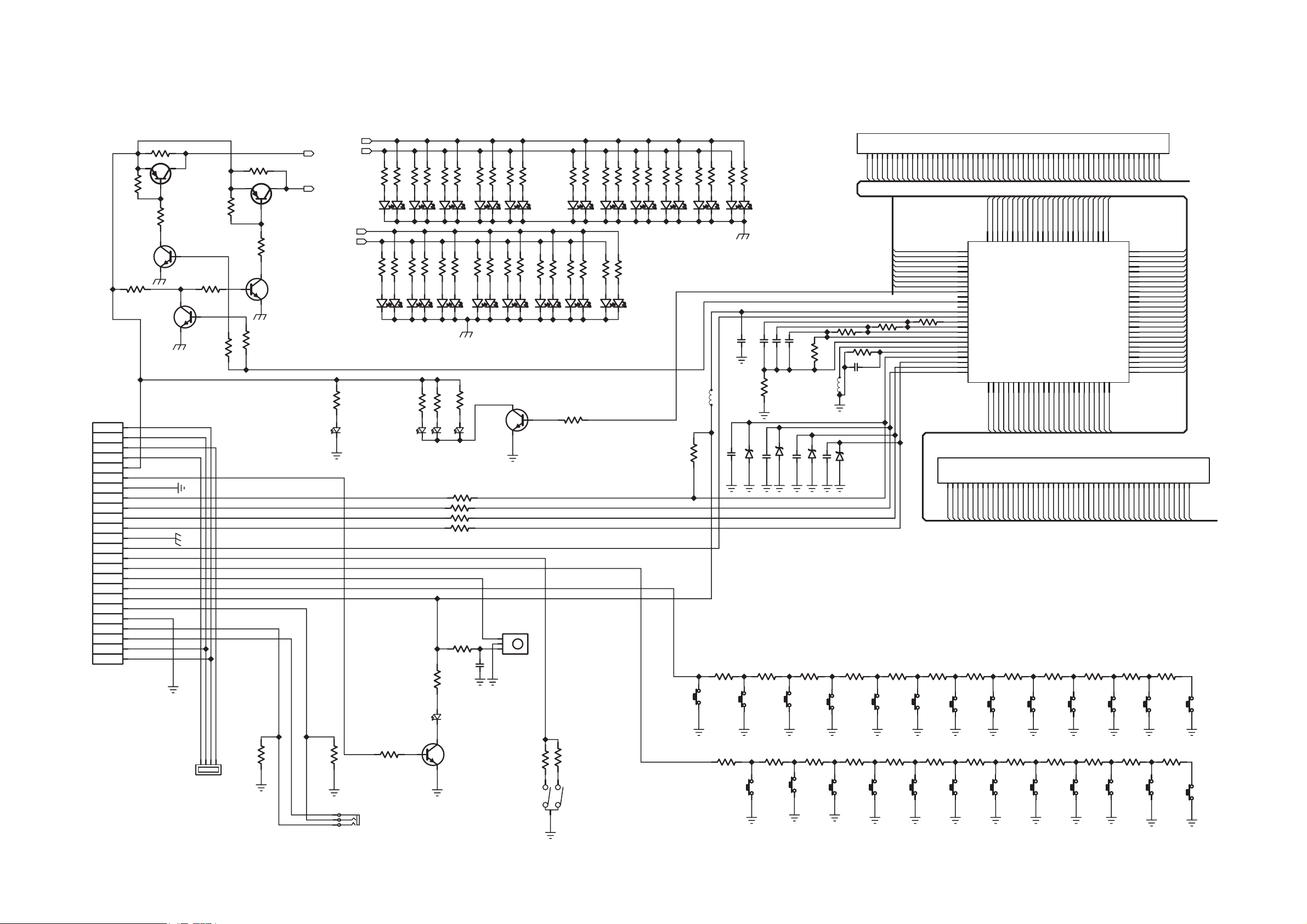
CIRCUIT DIAGRAM - SERVO BOARD
PART 1
7 - 1
7 - 1
Page 19
CIRCUIT DIAGRAM - SERVO BOARD
PART 2
7 - 2
7 - 2
Page 20
LAYOUT DIAGRAM - SERVO BOARD
TOP SIDE VIEW
7 - 3 7 - 3
Page 21
LAYOUT DIAGRAM - SERVO BOARD
BOTTOM SIDE VIEW
7 - 4 7 - 4
Page 22

Revision list
Version1.0 ( 3141 785 35010)
*Initial Release
Version1.1 ( 3141 785 35011)
*new -/51 added.
9 - 1
Page 23

TENTATIVE Version No.18052009
LV47002P Development Specification Proposal
(BTL 4 channel Car Audio Power Amplifier)
The LV47002P is the IC for 4-channel BTL power amplifier that is developed for car audio system.
Pch DMOS in the upper side of the output stage and Nch DMOS in the lower side of the output stage are
complimentary. High power and high quality sound are realized by that.
This IC incorporate various functions (standby switch, muting function, and various protection circuit) necessary for
car audio system. Also, it has a self-diagnosis function.
1. Application : 4-channel BTL power amplifier for car audio system
2. Package type : HZIP25
3. Functions and Features :
- High power : - Pomax=48W (typical)
(Vcc=15.2V, f=1kHz , JEITAmax , RL=4Ω)
- Po = 28W (typical)
(Vcc=14.4V, f=1kHz , THD=10% , RL=4Ω)
- Po = 21W (typical)
(Vcc=14.4V, f=1kHz , THD=1% , RL=4Ω)
- Built-in muting function (pin 22)
- Built-in Standby switch function (pin 4)
- Built-in Self-diagnosis function (pin 25) : Signal output in case of output offset detection, shorting to VCC,
shorting to ground , and load shorting.
- Electric mirror noise decrease
- Built-in various protection circuit (shorting to ground, shorting to VCC, load shorting, over voltage and
thermal shut down )
- No external anti-oscillation part necessary.
Note1 : Please do not mistake connection.
A wrong connection may produce destruction, deterioration and damage for the IC or equipment.
Note2 : The protective circuit function is provided to temporarily avoid abnormal state such as incorrect output
connection. But, there is no guarantee that the IC is not destroyed by the accident.
The protective function do not operate of the operation guarantee range. If the outputs are connected
incorrectly, IC destruction may occur when used outside of the operation guarantee range.
Note3 : External parts, such as the anti-oscillation part, may become necessary depending on the set condition.
Check their necessity for each set.
Page 24
TENTATIVE 2
4. Maximum Ratings at Ta = 25℃℃℃℃
Parameter Symbol Conditions Ratings Unit
Maximum supply Voltage Vcc max 1 No signal, t=1 minute 26 V
Vcc max 2 During operations 18 V
Maximum output current Io peak Per channel 4.5/ch A
Allowable Power dissipation Pd max With an infinity heat sink 50 W
Operating temperature Topr -40 to 85 ℃
Storage temperature Tstg -40 to 150 ℃
Thermal resistance between the junction and case
5. Recommended operating range at Ta=25℃℃℃℃
Parameter Symbol Conditions Ratings Unit
Recommended supply voltage Vcc 14.4 V
Recommended load resistance RL op 4 Ω
Operating supply voltage range Vcc op A range not exceeding Pdmax 9 to 16 V
6. Electrical Characteristics at Ta=25℃℃℃℃, Vcc=14.4V, RL=4Ω, f=1kHz, Rg=600Ω
Parameter Symbol
Quiescent current Icco RL=∞, Rg=0Ω 200 400 mA
Standby current Ist Vst=0V 10 uA
Voltage gain VG Vo=0dBm 25 26 27 dB
Voltage gain difference ∆VG -1 +1 dB
Output power Po THD=10% 23 28 W
Pomax1 JEITA max 43 W
Pomax2 Vcc=15.2,JEITA max 48 W
θj-c 1 ℃/W
Conditions min typ max Unit
Output offset voltage Vn offset Rg=0Ω -100 +100 mV
Total harmonic distortion THD Po=4W 0.03 0.2 %
Channel separation CHsep Vo=0dBm, Rg=10kΩ 55 65 dB
Ripple rejection ratio SVRR Rg=0Ω, fr=100Hz , Vccr=0dBm 45 65 dB
Output noise voltage VNO Rg=0Ω, B.P.F.=20Hz to 20kHz 80 200 uVrms
Input resistance Ri 40 50 65 kΩ
Mute attenuation Matt Vo=20dBm ,MUTE : ON 75 90 dB
Vstby H AMP : ON 2.5 Vcc V Standby Pin
Control voltage
Control voltage
Output offset detection
Detection threshold voltage Vosdet ±1.2 ±1.8 ±2.4 V
Note : 0dBm = 0.775Vrms
Vstby L
Vmute H MUTE : OFF OPEN - Mute Pin
Vmute L
AMP : OFF 0.0 0.5 V
MUTE : ON 0.0 1.5 V
Note : Information in this document is subject to change without notice.
Page 25
TENTATIVE 3
7. LV47002P Test and Application circuit
a
cc
cc
cc
L
D
ile
ilter
rotective
circit
D
L
D
D
D
te
circit
te
D
Lo Level
te
L
tan
itch
rotective
circit
D
D
L
The components and constant values within the test circuit are used for confirmation of characteristics
and are not guarantees that incorrect or trouble will not occur in application equipment.
Note : Information in this document is subject to change without notice.
Page 26

TENTATIVE 4
8. Explanation for the functions
1. Standby switch function (pin 4)
Threshold voltage of the pin 4 is set by about 2VBE.
The amplifier is turned on by the applied voltage of 2.5V or more. Also, the amplifier is turned off by the applied
voltage of 0.5V or less.
2. Muting function (pin 22)
Fig1 Standby equivalent circuit
The muted state is obtained by setting pin 22 to the ground potential, enabling audio muting.
The muting function is turned on by the applied voltage of 1V or less to the resistance of 10kΩ. And the muting
function is turn off when this pin opens.
Also, the time constant of the muting function is determined by external capacitor and resistor constants.
It is concerned with a pop noise in amplifier ON/OFF and mute ON/OFF. After enough examination, please set it.
Fig2 Mute equivalent circuit
3. ACGND pin (pin 16)
The capacitor of the pin 16 must use the same capacitance value as the input capacitor.
Also, connect to the same PREGND as the input capacitor.
Note : Information in this document is subject to change without notice.
Page 27

TENTATIVE 5
4. Self-diagnosis function (pin 25)
By detecting the unusual state of the IC, the signal is output to the pin 25.
Also, by controlling the standby switch after the signal of the pin 25 is detected by the microcomputer,
the burnout of the speaker can be prevented.
1) Shorting to VCC / Shorting to ground : The pin 25 becomes the low level.
2) Load shorting : The pin 25 is alternated between the low level and the high level according to the output signal.
3) Output offset detection : when the output offset voltage exceeds the detection threshold voltage,
the pin 25 becomes the low level.
* Note: The output offset abnormality is thought of as the leakage current of the input capacitor.
In addition, the pin 25 has become the NPN open collector output (active low).
The pin 25 must be left open when this function is not used.
5. Sound Quality (low frequencies)
By varying the value of input capacitor, low-frequency characteristic can be improved.
However, it is concerned the shock noise. Please confirm in each set when the capacitance value varies.
6. Pop noise
For pop noise prevention, it is recommended to use the muting function at the same time.
- Please turn on the muting function simultaneously with power supply on when the amplifier is
turned on. Next, turn off the muting function after the output DC potential stabilization.
- When the amplifier is turn off, turn off the power supply after turning on the muting function.
. Oscillation Stability
Pay due attention on the following points because parasitic oscillation may occur due to effects of the capacity
load, board layout, etc.
(1) Capacity load
When the capacitor is to be inserted between each output pin and GND so as to prevent electric mirror noise,
select the capacitance of maximum 1500 pF. (Conditions: Our recommended board, RL = 4Ω)
(2) Board layout
- Provide the VCC capacitor of 0.1µF in the position nearest to IC.
- PREGND must be independently wired and connected to the GND point that is as stable as possible,
such as the minus pin of the 2200µF VCC capacitor.
In case of occurrence of parasitic oscillation, any one of following parts may be added as a countermeasure.
Note that the optimum capacitance must be checked for each set in the mounted state.
- Series connection of CR (0.1µF and 2.2Ω) between BTL outputs
- Series connection of CR(0.1µF and 2.2Ω) between each output pin and GND.
Note : Information in this document is subject to change without notice.
Page 28

TENTATIVE 6
250
RL=Open
200
R=0Ω
150
100
Icco (mA)
50
0
6 8 10 12 14 16 18
Icco - Vcc
Vcc (V)
14
RL=Open
R=0Ω
8
6
4
2
0
6 8 10 12 14 16 18
(V)
N
V
12
10
Vcc (V)
VN - Vcc
50
f=1kHz
RL=4Ω
40
THD=10%
30
20
Po (W)
Po - Vcc(THD=10%)
all channel is similar
10
0
8 10 12 14 16 18
Vcc (V)
10
1
THD - Po(f=1kHz)
Vcc=14.4V
RL=4Ω
f=1kHz
ch1
ch2
ch3
ch4
THD (%)
0.1
25
20
all channel is similar
15
10
Po (W)
Vcc=14.4V
RL=4Ω
5
THD=1%
0
10 100 1000 10000 100000
f (Hz)
Po - f(THD=1%)
10
1
THD - Po(f=100Hz)
Vcc=14.4V
RL=4Ω
f=100Hz
ch1
ch2
ch3
ch4
THD (%)
0.1
0.01
0.1 1 10 100
Po (W)
THD - Po(f=10kHz)
10
Vcc=14.4V
RL=4Ω
f=10kHz
1
THD (%)
0.1
0.01
0.1 1 10 100
ch1
ch2
ch3
ch4
Po (W)
0.01
0.1 1 10 100
Po (W)
THD - f
10
Vcc=14.4V
RL=4Ω
Po=4W
1
THD (%)
0.1
0.01
10 100 1000 10000 100000
f (Hz)
Note : Information in this document is subject to change without notice.
ch1
ch2
ch3
ch4
Page 29

TENTATIVE 7
1
0
all channel is similar
-1
Vcc=14.4V
-2
Response (dB)
RL=4Ω
Vo=0dBm
-3
10 100 1000 10000 100000
f (Hz)
f-Response
150
Vcc=14.4V
RL=4Ω
100
(µVrms)
NO
50
V
0
10 100 1000 10000 100000
VNO - Rg
ch1
ch2
ch3
ch4
Rg (Ω
80
60
40
Vcc=14.4V
CH.sep (dB)
RL=4Ω
20
Rg=10kΩ
Vo=0dBm
0
10 100 1000 10000 100000
CH.Sep - f(CH1→→→→)
ch1→ch2
ch1→ch3
ch1→ch4
f (Hz)
80
60
40
Vcc=14.4V
RL=4Ω
CH.sep (dB)
20
Rg=10kΩ
Vo=0dBm
0
10 100 1000 10000 100000
CH.Sep - f(CH3
→→→→
)
ch3→ch1
ch3→ch2
ch3→ch4
f (Hz)
80
60
40
Vcc=14.4V
RL=4Ω
CH.sep (dB)
20
Rg=10kΩ
Vo=0dBm
0
10 100 1000 10000 100000
CH.Sep - f(CH2→→→→)
ch2→ch1
ch2→ch3
ch2→ch4
f (Hz)
80
60
40
Vcc=14.4V
RL=4Ω
CH.sep (dB)
20
Rg=10kΩ
Vo=0dBm
0
10 100 1000 10000 100000
CH.Sep - f(CH4→→→→)
ch4→ch1
ch4→ch2
ch4→ch3
f (Hz)
80
60
40
VccR=0dBm
fR=100Hz
Rg=0Ω
SVRR (dB)
RL=4Ω
20
CVcc=0.1μF
0
8 10 12 14 16 18
SVRR - Vcc
Vcc (V)
ch1
ch2
ch3
ch4
80
60
40
SVRR (dB)
20
Vcc=14.4V
VccR=0dBm
Rg=0Ω
RL=4Ω
CVcc=0.1μF
0
10 100 1000 10000 100000
SVRR - f
fR (Hz)
Note : Information in this document is subject to change without notice.
R
ch1
ch2
ch3
ch4
Page 30

TENTATIVE 8
4
RL=4Ω
R=0Ω
3
2
Vosdet (V)
1
Offset DIAG - Vcc
Detection Level
60
f=1kHz
RL=4Ω
50
Pd=Vcc×Icc-Po×4ch
40
30
Pd (W)
20
10
Pd - Po
Vcc=14.4V
Vcc=16V
0
8 10 12 14 16 18
Vcc (V)
250
200
150
100
Vcc=14.4V
RL=Open
R=0Ω
Icco - Vst
Icco (mA)
50
0
0.0 1.0 2.0 3.0 4.0 5.0
Vst (V)
0
0.1 1 10 100
Po (W)
100
80
60
40
Mute ATT(dB)
20
0
0.0 1.0 2.0 3.0 4.0 5.0
Mute ATT - V Mute
Vcc=14.4V
RL=4Ω
Vo=20dBm
V Mute(V)
Note : Information in this document is subject to change without notice.
Page 31

Page 32

TDA7419
Fi
3 BAND CAR AUDIO PROCESSOR
PRELIMINARY DATA
1 FEATURES
■ 4 STEREO INPUTS
■ SOFT STEP VOLUME
■ BASS, MIDDLE, TREBLE AND LOUDNESS
■ DIRECT MUTE AND SOFTMUTE
■ FOUR INDEPENDENT SPEAKER OUTPUTS
■ SUB WOOFER OUTPUT
■ SOFT STEP SPEAKER/SUBWOOFER
CONTROL
■ 7 BANDS SPECTRUM ANALYZER
■ DIGITAL CONTROL:
2
–I
C-BUS INTERFACE
2 DESCRIPTION
The TDA7419 is a high performance signal processor specifically designed for car radio applications.
The device includes a high performance audiopro-
Figure 2. Block Diagram
MUTE
SAOUT SACLK
SAOUT SACLK
Spectrum
Spectrum
Analyzer
Analyzer
MUTE
gure 1. Package
SO-28
Table 1. Order Codes
Part Number Package
TDA7419 SO-28
TDA7419TR SO-28 in Tape & Reel
cessor with fully integrated audio filters. The digital
control allows programming in a wide range of filter
characteristics. By the use of BICMOS-process and
linear signal processing low distortion and low noise
are obtained.
ACOUTL/
ACOUTR/
ACINL/
ACOUTL/
AC2OUTL
AC2OUTL
ACOUTR/
AC2OUTR
AC2OUTR
ACINL/
FILOL
FILOL
ACINR/
ACINR/
FILOR
FILOR
DIFFL
DIFFL
DIFFG
DIFFG
DIFFR
DIFFR
SE1L
SE1L
SE1R
SE1R
SE2L
SE2L
SE2R
SE2R
INPUT
INPUT
MULTIPLEXER
MULTIPLEXER
SUPPLY
SUPPLY
VDD CREFGND
VDD CREFGND
InGain
InGain
AutoZero
AutoZero
VREFOUTF
VREFOUTF
Loudness MiddleTreble BassSoftMute
Loudness MiddleTreble BassSoftMute
DIGITAL CONTROL
DIGITAL CONTROL
DIGITAL CONTROL
Softstep
Softstep
Volume
Volume
I2C BUS
I2C BUS
I2C BUS
Subwoofer
Subwoofer
LPF
LPF
AC2INL/
SDASCL
SDASCL
AC2INL/
SE3L
SE3L
AC2INR/
AC2INR/
SE3R
SE3R
Softste p
Softste p
MonoFader
MonoFader
Softstep
Softstep
MonoFader
MonoFader
Softstep
Softstep
MonoFader
MonoFader
Softstep
Softstep
MonoFader
MonoFader
Softste p
Softste p
MonoFader
MonoFader
Softstep
Softstep
MonoFader
MonoFader
HPF
HPF
HPF
HPF
Mix
Mix
Mix
Mix
November 2004
This is preliminary information on a new product now in development or undergoing evaluation. Details are subject to change without notice.
OUTLF
OUTLF
OUTRF
OUTRF
OUTLR
OUTLR
OUTRR
OUTRR
OUTSW/
OUTSW/
OUTLR2
OUTLR2
MIX/
MIX/
OUTSW/
OUTSW/
OUTRR2
OUTRR2
Rev. 1
1/30
Page 33

TDA7419
Table 2. Supply
Symbol Parameter Test Condition Min. Typ. Max. Unit
Supply Voltage 7.5 8.5 10.5 V
V
s
Supply Current Vs = 8.5V 30 35 40 mA
I
s
SVRR Ripple Rejection @ 1KHz Audioprocessor(all Filters flat) 60 dB
Table 3. Thermal Data
Symbol Parameter Value Unit
R
Th j-pins
Thermal Resistance Junction-pins max 85 °C/W
Table 4. Absolute Maximum Ratings
Symbol Parameter Value Unit
Operating Supply Voltage 10.5 V
V
s
T
T
Operating Temperature Range -40 to 85 °C
amb
Storage Temperature Range -55 to +150 °C
stg
ESD
All pins are protected against ESD according to the MIL883 standard.
Figure 3. Pin connection (Top view)
ACOUTR/AC2OUTR
ACINR/FILOR
ACINL/FILOL
ACOUTL/AC2OUTL
SE3L/ACINL
SE3R/ACINR
SE2L
SE2R
SE1L OUTLF
SE1R OUTLR
DIFFL
DIFFG
DIFFR OUTSW/OUTLR2
2
3
4
5
6
7
8
9
10
12
13
28
27
26
25
24
23
22
21
20
19
18
17
16
1514CREF GND
D04AU1569
MIX/OUTSW/OUTRR21
VREF
SAOUT
SAIN
VDD
SDA
SCL
MUTE
OUTRR11
OUTRF
2/30
Page 34

Table 5. Pin Description
TDA7419
Pin
N#
1 ACOUTR / AC2OUTR AC coupling right output / DSO filter AC2OUT right channel O
2 ACINR / FILOR AC coupling right input / DSO filter FILO right channel I/O
3 ACINL / FILOL AC coupling left input / DSO filter FILO left channel I/O
4 ACOUTL / AC2OUTL AC coupling left output / DSO filter AC2OUT left channel O
5 SE3L / ACINL Single-ended input 3 left channel / AC coupling left input I
6 SE3R / ACINR Single-ended input 3 right channel / AC coupling right input I
7 SE2L Single-ended input 2 left channel I
8 SE2R Single-ended input 2 right channel I
9 SE1L Single-ended input 1 left channel I
10 SE1R Single-ended input 1 Right channel I
11 DIFFL Pseudo differential stereo input left I
12 DIFFG Pseudo differential stereo input common I
13 DIFFR Pseudo differential stereo input right I
14 CREF Reference capacitor O
15 GND Ground S
16 OUTSW / OUTLR2
17 OUTRF Front right output O
18 OUTRR Rear right output O
19 OUTLR Rear left output O
20 OUTLF Front left output O
21 MUTE External mute pin I
22 SCL I2C bus clock I
23 SDA I2C bus data I/O
24 VDD Supply S
25 SAIN Spectrum analyzer clock input I
26 SAOUT Spectrum analyzer output O
27 VREF Vref output O
28 MIX / OUTSW / OUTRR2
Pin Name Function I/O
Subwoofer output / 2
Mix input / Additional subwoofer output / 2
nd
rear left output
nd
rear right output
I/O
O
3/30
Page 35

TDA7419
3 Audio Processor Features:
Input Multiplexer QD / SE: quasi-differential stereo inputs, with selectable single-ended mode
SE1: stereo single-ended input
SE2: stereo single-ended input
SE3 / AC2IN: stereo single-ended input / DSO filter input
In-Gain 0 to 15dB, 1dB steps
internal offset-cancellation (AutoZero)
separate second source-selector
Mixing stage mixable to front speaker-outputs
Loudness 2nd order frequency response
programmable center frequency (400Hz/800Hz/2400Hz)
15dB with 1dB steps
selectable low & high frequency boost
selectable flat-mode (constant attenuation)
Volume +15dB to -79dB with 1dB step resolution
soft-step control with programmable blend times
Bass 2nd order frequency response
center frequency programmable in 4 steps (60Hz/80Hz/100Hz/200Hz)
Q programmable 1.0/1.25/1.5/2.0
DC gain programmable
-15 to 15dB range with 1dB resolution
Middle 2nd order frequency response
center frequency programmable in 4 steps (500Hz/1KHz/1.5KHz/2.5KHz)
Q programmable 0.5/0.75/1.0/1.25
DC gain programmable
-15 to 15dB range with 1dB resolution
Treble 2nd order frequency response
center frequency programmable in 4 steps (10KHz/12.5KHz/15KHz/17.5KHz)
-15 to 15dB range with 1dB resolution
Spectrum analyzer seven bandpass filters
2nd order frequency response
programmable Q factor for different visual appearance
analog output
controlled by external serial clock
Speaker 4 independent soft step speaker controls, +15dB to -79dB with 1dB steps
Independent programmable mix input with 50% mixing ratio for front speakers
direct mute
Subwoofer 2nd order low pass filter with programmable cut off frequency
single-ended mono output
independent soft step level control, +15dB to -79dB with 1dB steps
Mute Functions direct mute
digitally controlled SoftMute with 3 programmable mute-times(0.48ms/0.96ms/
123ms)
Effect gain effect, or high pass effect with fixed external components
4/30
Page 36

TDA7419
4 ELECTRICAL CHARACTERISTICS
Table 6. Electrical Characteristcs
V
= 8.5V; T
S
Symbol Parameter Test Condition Min. Typ. Max. Unit
INPUT SELECTOR
R
in
V
CL
S
IN
G
IN MIN
G
IN MAX
G
STEP
V
DC
V
offset
DIFFERENTIAL STEREO INPUTS
R
in
CMRR Common Mode Rejection Ratio V
e
No
MIXING CONTROL
M
LEVEL
G
MAX
A
MAX
A
STEP
LOUDNESS CONTROL
A
MAX
A
STEP
f
Peak
VOLUME CONTRO L
G
MAX
A
MAX
A
STEP
E
A
E
T
V
DC
SOFT MUTE
A
MUTE
= 25°C; RL= 10kΩ ; all gains = 0dB; f = 1kHz; unless otherwise specified
amb
Input Resistance All single ended inputs 70 100 130 kΩ
Clipping level 2 V
Input Separation 80 100 dB
Min. Input Gain 0 dB
Max. Input Gain 15 dB
Step Resolution 1 dB
DC Steps Adjacent Gain Steps 1 mV
G
MIN
to G
MAX
4mV
Remaining offset with AutoZero 0.5 mV
Input Resistance Differential 70 100 KΩ
=1 VRMS@ 1kHz 46 70 dB
CM
=1 VRMS@ 10kHz 46 60 dB
V
CM
Output Noise @ Speaker Outputs 20Hz-20kHz,flat;all stages 0dB 12 µV
Mixing Ratio Main / Mix Source -6/-6 dB
Max Gain 13 15 17 dB
Max Attenuation -83 -79 -75 dB
Step Resolution 0.5 1 1.5 dB
Max Attenuation 15 dB
Step Resolution 1 dB
Peak Frequency
f
P1
f
P2
f
P3
400 Hz
800 Hz
2400 Hz
Max Gain 15 dB
Max Attenuation -79 dB
Step Resolution 0.5 1 1.5 dB
Attenuation Set Error G = -20 to +20dB -0.75 0 +0.75 dB
G = -79 to -20dB -4 0 3 dB
Tracking Error 2dB
DC Steps Adjacent Attenuation Steps 0.1 3 mV
From 0dB to G
MIN
0.5 5 mV
Mute Attenuation 80 100 dB
RMS
5/30
Page 37

TDA7419
Table 6. Electrical Characteristcs (continued)
= 8.5V; T
V
S
Symbol Parameter Test Condition Min. Typ. Max. Unit
T
D
V
TH Low
V
TH High
R
PU
V
PU
BASS CONTROL
Fc Center Frequency f
Q
BASS
C
RANGE
A
STEP
DC
GAIN
MIDDLE CONTROL
C
RANGE
A
STEP
f
c
Q
BASS
TREBLE CONTROL
C
RANGE
A
STEP
fc Center Frequency f
SPEAKER ATTENUATORS
G
MAX
= 25°C; RL= 10kΩ ; all gains = 0dB; f = 1kHz; unless otherwise specified
amb
Delay Time T1 0.48 1 ms
T2 0.96 2 ms
T3 70 123 170 ms
Low Threshold for SM Pin 1 V
High Threshold for SM Pin 2.5 V
Internal pull-up resistor 32 45 58
Internal pull-up Voltage 3.3 V
54 60 66 Hz
72 80 88 Hz
90 100 110 Hz
180 200 220 Hz
0.911.1
1.1 1.25 1.4
1.3 1.5 1.7
1.822.2
Quality Factor Q
C1
f
C2
f
C3
f
C4
1
Q
2
Q
3
Q
4
Control Range ±14 ±15 ±16 dB
Step Resolution 0.5 1 1.5 dB
Bass-DC-Gain DC = off -1 0 +1 dB
DC = on (shelving filter, use for
-4.4 dB
cut only)
Control Range ±14 ±15 ±16 dB
Step Resolution 0.5 1 1.5 dB
Center Frequency f
Quality Factor Q
C1
f
C2
f
C3
f
C4
1
Q
2
Q
3
Q
4
400 500 600 Hz
0.811.2kHz
1.2 1.5 1.8 kHz
22.53kHz
0.45 0.5 0.55
0.65 0.75 0.85
0.911.1
1.1 1.25 1.4
Clipping Level ±14 ±15 ±16 dB
Step Resolution 0.5 1 1.5 dB
C1
f
C2
f
C3
f
C4
81012kHz
10 12.5 15 kHz
12 15 18 kHz
14 17.5 21 kHz
Max Gain 14 15 16 dB
kΩ
6/30
Page 38

TDA7419
Table 6. Electrical Characteristcs (continued)
= 8.5V; T
V
S
Symbol Parameter Test Condition Min. Typ. Max. Unit
A
MAX
A
STEP
A
MUTE
E
E
V
DC
AUDIO OUTPUTS
V
CL
R
OUT
R
L
C
L
V
DC
SUBWOOFER ATTENUATOR
G
MAX
A
MAX
A
STEP
A
MUTE
E
E
V
DC
SUBWOOFER LOWPASS
f
LP
HPF EFFECT
G
MAX
G
MIN
A
STEP
SPECTRUM ANALYZER CONTROL
V
SAOut
f
C1
f
C2
f
C3
f
C4
f
C5
f
C6
f
C7
Q Quality Factor Q1 1.8
f
SAClk
t
Sadel
t
repeat
t
intres
= 25°C; RL= 10kΩ ; all gains = 0dB; f = 1kHz; unless otherwise specified
amb
Max Attenuation -83 -79 -75 dB
Step Resolution 0.5 1 1.5 dB
Mute Attenuation 80 90 dB
Attenuation Set Error 2dB
DC Steps Adjacent Attenuation Steps 0.1 5 mV
Clipping level d = 0.3% 2 V
Output impedance 30 100 Ω
Output Load Resistance 2 kΩ
Output Load Capacitor 10 nF
DC Voltage Level 3.8 4.0 4.2 V
Max Gain 14 15 16 dB
Max Attenuation -83 -79 -75 dB
Step Resolution 0.5 1 1.5 dB
Mute Attenuation 80 90 dB
Attenuation Set Error 2dB
DC Steps Adjacent Attenuation Steps 1 5 mV
Lowpass Corner Frequency f
f
f
LP1
LP2
LP3
72 80 88 Hz
108 120 132 Hz
144 160 176 Hz
Max Gain 22 dB
Min Gain 4dB
Step Resolution 2 dB
Output Voltage Range 0 3.3 V
Center Frequency Band 1 62 Hz
Center Frequency Band 2 157 Hz
Center Frequency Band 3 392 Hz
Center Frequency Band 4 1 kHz
Center Frequency Band 5 2.51 kHz
Center Frequency Band 6 6.34 kHz
Center Frequency Band 7 16 kHz
Q2 3.5
Clock Frequency 1 100 kHz
Analog Output Delay Time 2 µs
Spectrum Analyzer Repeat Time 50 ms
Internal Reset Time 4.5 ms
RMS
7/30
Page 39

TDA7419
Table 6. Electrical Characteristcs (continued)
= 8.5V; T
V
S
Symbol Parameter Test Condition Min. Typ. Max. Unit
GENERAL
e
NO
S/N Signal to Noise Ratio all gain = 0dB flat; Vo =2V
DDistortion V
S
C
= 25°C; RL= 10kΩ ; all gains = 0dB; f = 1kHz; unless otherwise specified
amb
Output Noise BW=20Hz to 20 kHz all gain =
12 µV
0dB
BW=20Hz to 20 kHz Output
6 µV
muted
100 dB
= 1V
IN
RMS
; all stages 0dB 0.01 %
RMS
Channel Separation left/right 90 dB
5 DESCRIPTION OF THE AUDIOPROCESSOR
5.1 Input stages
In the basic configuration, one stereo quasi-differential and three (two in case of DSO applications) single
ended stereo inputs are available.
5.1.1 Quasi-differential stereo Input (QD)
The QD input is implemented as a buffered quasi-differential stereo stage with 100k input-impedance at
each input. The attenuation is fixed to -3dB in order to adapt the incoming signal level.
5.1.2 Single-ended stereo input (SE1, SE2, SE3/AC2IN)
The input-impedance at each input is 100k and the attenuation is fixed to -3dB for incoming signals. The
input for SE3 is also configurable as part of the interface for external filters in DSO applications (AC2IN)
Figure 4. Input Stage
QD_L
QD_G
QD_R
SE1_L
SE1_R
SE2_L
SE2_R
AC2IN_L/SE3L
AC2IN_R/SE3R
QD
SE1
SE2
SE3
QD
SE4
SE1
SE2
SE3
Main
Source
In Gain
Second
Source
8/30
Output Stage
Page 40

TDA7419
5.2 AutoZero
The AutoZero allows a reduction of the number of pins as well as external components by canceling any
offset generated by or before the In-Gain-stage (Please notice that externally generated offsets, e.g. generated through the leakage current of the coupling capacitors, are not canceled).
The auto-zeroing is started every time the input source is changed and needs max. 0.3ms for the alignment. To avoid audible clicks the Audio processor is muted before the loudness stage during this time.
The AutoZero feature is only present in the main signal-path.
5.2.1 AutoZero-Remain
In some cases, for example if the P is executing a refresh cycle of the IIC-Bus-programming, it is not useful to start a new AutoZero-action because no new source is selected and an undesired mute would appear at the outputs. For such applications, it can be switched in the AutoZero-Remain-Mode (Bit 6 of the
subaddress-byte). If this bit is set to high, the AutoZero will not be invoked and the old adjustment-value
remains.
5.3 Loudness
There are four parameters programmable in the loudness stage:
5.3.1 Attenuation
Figure 5 shows the attenuation as a function of frequency at f
= 400Hz
P
Figure 5. Loudness Attenuation @ f
5
0
-5
-10
-15
-20
10
= 400Hz.
P
100
1K
10K
9/30
Page 41

TDA7419
5.3.2 Peakr Frequency
Figure 6 shows the three possible peak-frequencies 400Hz , 800Hz and 2.4kHz.
Figure 6. Loudness Center frequencies @ Attn. = 15dB
5
0
-5
-10
-15
-20
10
100
1K
5.3.3 Low & High Frequency Boost
Figure 7 shows the different Loudness-shapes in low & high frequency boost.
Figure 7. Loudness Attenuation , fC = 2.4KHz
5
0
-5
-10
-15
10K
10/30
-20
10
100
1K
10K
Page 42

5.3.4 Flat Mode
In flat mode the loudness stage works as a 0dB to -15dB attenuator.
TDA7419
5.4 SoftMute
The digitally controlled SoftMute stage allows muting/demuting the signal with a I
slope. The mute process can either be activated by the SoftMute pin or by the I
2
C-bus programmable
2
C-bus. This slope is real-
ized in a special S-shaped curve to mute slow in the critical regions (see Figure 8).
For timing purposes the Bit0 of the I2C-bus output register is set to 1 from the start of muting until the end
of demuting.
Figure 8. Sofmute Timing
1
EXT.
MUTE
+SIGNAL
REF
-SIGNAL
1
2
I
C BUS
OUT
D97AU634
Time
Note: Please notice that a started Mute-action is always terminated and could not be interrupted by a change of the mute -signal
5.5 SoftStep-Volume
When the volume-level is changed audible clicks could appear at the output. The root cause of those clicks
could either be a DC-Offset before the volume-stage or the sudden change of the envelope of the audiosignal. With the SoftStep feature both kinds of clicks could be reduced to a minimum and are no more
audible. The blend-time from one step to the next is programmable in four steps.
Figure 9. SoftStep Timing
V
OUT
1dB
0.5dB
SS Time
-0.5dB
-1dB
Note: For steps more than 0.5dB the SoftStep mode should be deactivated because it could generate a hard 1dB step during the blend-time.
D00AU1170
Time
11/30
Page 43

TDA7419
5.6 Bass
There are four parameters programmable in the bass stage:
5.6.1 Attenuation
Figure 9 shows the attenuation as a function of frequency at a center frequency of 80Hz.
Figure 10. Bass Control @ f
15.0
10.0
5.0
= 80Hz, Q = 1
C
dB
0.0
-5.0
-10.0
-15.0
10.0 100.0 1.0K 10.0K
Hz
5.6.2 Center Frequency
Figure 11 shows the four possible center frequencies 60, 80, 100 and 200Hz.
Figure 11. Bass center Frequencies @ Gain = 15dB, Q = 1
16
12
8
4
0
-4
10
12/30
100
1K
10K
Page 44

5.6.3 Quality Factors
Figure 12 shows the four possible quality factors 1, 1.25, 1.5 and 2.
Figure 12. Bass Quality factors @ Gain = 14dB, fC = 80Hz
15.0
12.5
10.0
7.5
5.0
2.5
TDA7419
0.0
10.0 100.0 1.0K 10.0K
5.6.4 DC Mode
It is used for cut only for shelving filter. In this mode the DC-gain is increased by 4.4dB. Inaddition the programmed center frequency and quality factor is decreased by 25% which can be used to reach alternative center frequencies or quality factors.
Figure 13. Bass normal and DC Mode @ Gain = 14dB, fC = 80Hz
15.0
12.5
10.0
7.5
5.0
2.5
0.0
10.0 100.0 1.0K 10.0K
Note: The center frequency, Q and DC-mode can be set fully independently.
13/30
Page 45

TDA7419
5.7 Middle
There are three parameters programmable in the middle stage:
5.7.1 Attenuation
Figure 14 shows the attenuation as a function of frequency at a center frequency of 1kHz.
Figure 14. Middle Control @ f
= 1 kHz, Q = 1
C
5.7.2 Center Frequency
Figure 14 shows the four possible center frequencies 500Hz, 1kHz, 1.5kHz and 2.5kHz.
Figure 15. Middle center Frequencies @ Gain = 14dB, Q = 1
14/30
Page 46

5.7.3 Quality Factors
Figure 16 shows the four possible quality factors 0.5, 0.75, 1 and 1.25.
Figure 16. Middle Quality factors @ Gain = 14dB, fc = 1kHz
TDA7419
5.8 Treble
There are two parameters programmable in the treble stage:
5.8.1 Attenuation
Figure 16 shows the attenuation as a function of frequency at a center frequency of 17.5kHz.
Figure 17. Treble Control @ f
20
15
10
5
0
-5
-10
-15
-20
10
= 17.5kHz
C
100
1K
10K
15/30
Page 47

TDA7419
5.8.2 Center Frequency
Figure 18 shows the four possible center frequencies 10k, 12.5k, 15k and 17.5kHz.
Figure 18. Treble Center Frequencies @ Gain = 15dB
20
15
10
5
0
-5
10
100
1K
10K
5.9 Subwoofer Filter
The subwoofer lowpass filter has butterworth characteristics with programmable cut-off frequency (80/
120/160Hz)
Figure 19. Subwoofer Control
16/30
Page 48

TDA7419
5.10 Spectrum Analyzer
A fully integrated seven-band spectrum analyzer with programmable quality factor is present. The spectrum analyzer consists of seven band pass filters with rectifier and sample capacitor that stores the maximum peak signal level since the last read cycle. This peak signal level can be read by a microprocessor
at the SAout-pin. To allow easy interfacing to an analog port of the microprocessor, the output voltage at
this pin is referred to device ground.
The microprocessor starts a read cycle with the negative going clock edge at the SAclk input. On the following positive clock edges, the peak signal level for the band pass filters is subsequently switched to
SAout. Each analog output data is valid after the time t
whenever SAclk remains high for the time t
. Note that a proper reset requires the clock signal SAclk
intres
to be held at high potential. Figure 20 shows the block diagram and figure 21 illustrates the read cycle
timing of the spectrum analyzer.
Figure 20. Spectrum analyzer block diagram
. A reset of the sample capacitors is induced
Sadel
Figure 21. Timing of the spectrum analyzer
17/30
Page 49

TDA7419
5.11 AC-Coupling
In some applications additional signal manipulations are desired, such as additional band equalizations.
For this purpose, an AC-Coupling can be placed before the loudness attenuator or speaker-attenuators,
which can be activated or internally shorted by I
attenuator is available at the AC-Outputs. The input-impedance of this AC-Inputs is 50kΩ.
Figure 22. Diagram of AC coupling
2
C-Bus. In short condition, the input-signal of the speaker-
ACINR
Speakers
To Output
From Input MUX
InGain
ACOUTR ACOUTL
Filters
ACINL
5.12 DSO Applications
For DSO applications, DSO filter is available for additional processing after the speaker control. It is a 2nd
order Butterworth highpass filter with selectable flat mode. Figure 23 shows the diagram of the DSO that
includes an external RC network.
Figure 23. DSO diagram
External RC network
From speaker
18/30
ACOUT
/AC2OUT
SE3IN
/AC2IN
ACIN
/FILO
Gain Control
To
output
Page 50

TDA7419
5.13 Output Selector and Mixing
The output-selector allows the front and rear speakers to connect to different sources. The setup of the
output selector is shown in Figure 24. A Mixing-stage is placed after the front speaker-attenuator and can
be set to mixing-mode. Having a full volume-attenuator for the mix-signal, the stage offers a wide flexibility
to adapt the mixing levels.
Figure 24. Output Selector
Mix_in
Attenuator
Main
Second
BassL+BassR
Attenuator
Attenuator
Subwoofer
filter
Attenuator
Front
Rear
Subwoofer
output
5.14 Audioprocessor Testing
In the test mode, which can be activated by setting bit D7 of the IIC subaddress byte and bit D0 of the
testing audioprocessor byte, several internal signals are available at the SE1R pin. In this mode, the input
resistance of 100kOhm is disconnected from the pin. Internal signals available for testing are listed in the
data-byte specification.
5.15 Test Circuit
Figure 25. Test Circuit
19/30
Page 51

TDA7419
6I2C BUS SPECIFICATION
6.1 Interface Protocol
The interface protocol comprises:
– a start condition (S)
– a chip address byte (the LSB determines read/write transmission)
– a subaddress byte
– a sequence of data (N-bytes + acknowledge)
– a stop condition (P)
– the max. clock speed is 500kbits/s
– 3.3V logic compatible
6.1.1 Receive Mode
S 1 0 0 0 1 0 0 R/W ACK TS AZ AI A4 A3 A2 A1 A0 ACK DATA ACK P
S = Start
R/W = "0" -> Receive Mode (Chip can be programmed by µP)
"1" -> Transmission Mode (Data could be received by µP)
ACK = Acknowledge
P = Stop
TS = Testing mode
AZ = Auto zero remain
AI = Auto increment
6.1.2 Transmission Mode
1 0 0 0 1 0 0 R/W ACK X X X X X X X SM ACK P
S
SM = Soft mute activated for main channel
X = Not Used
The transmitted data is automatic updated after each ACK. Transmission can be repeated without new
chip address.
6.1.3 Reset Condition
A Power-On-Reset is invoked if the Supply-Voltage is below than 3.5V. After that the following data is written automatically into the registers of all subaddresses:
MSB LSB
11111110
20/30
Page 52

6.2 Subaddress (receive mode)
Table 7. Subaddress (receive mode)
MSB LSB FUNCTION
I2 I1 I0 A4 A3 A2 A1 A0
0
1
0
1
0
1
0 0 0 0 0 Main Source Selector
0 0 0 0 1 Main Loudness
0 0 0 1 0 Soft Mute / Clock Generator
000 1 1Volume
001 0 0Treble
001 0 1Middle
001 1 0Bass
0 0 1 1 1 Second Source Selector
0 1 0 0 0 Subwoofer / Middle / Bass
0 1 0 0 1 Mixing / Gain Effect
0 1 0 1 0 Speaker Attenuator Left Front
0 1 0 1 1 Speaker Attenuator Right Front
0 1 1 0 0 Speaker Attenuator Left Rear
0 1 1 0 1 Speaker Attenuator Right Rear
0 1 1 1 0 Mixing Level Control
0 1 1 1 1 Subwoofer Attenuator
1 0 0 0 0 Spectrum Analyzer / Clock Source / AC Mode
1 0 0 0 1 Testing Audio Processor
Testing Mode
Off
On
Auto Zero Remain
Off
On
Auto Increment Mode
Off
On
TDA7419
21/30
Page 53

TDA7419
6.3 Data Byte Specification
Table 8. Main Selector (0)
MSB LSB FUNCTION
D7 D6 D5 D4 D3 D2 D1 D0
0
0
0
0
1
1
1
0
0
:
1
1
0
1
0
0
:
1
1
0
0
:
1
1
0
1
:
0
1
0
0
1
1
0
0
1
Source Selector
0
QD/SE: QD
1
SE1
0
SE2
1
SE3
0
QD/SE: SE
1
mute
x
mute
Input Gain
0dB
1dB
:
14dB
15dB
Auto Zero
on
off
Table 9. Main Loudness (1)
MSB LSB FUNCTION
D7 D6 D5 D4 D3 D2 D1 D0
0
0
:
1
1
0
0
1
1
0
1
0
1
0
1
0
1
0
0
:
1
1
0
0
:
1
1
Attenuation
0
0dB
1
-1dB
:
:
0
-14dB
1
-15dB
Center Frequency
Flat
400Hz
800Hz
2400Hz
High Boost
on
off
Loudness Soft Step
on
off
22/30
Page 54

Table 10. Soft Mute / Clock Generator (2)
MSB LSB FUNCTION
D7 D6 D5 D4 D3 D2 D1 D0
Soft Mute
0
on
1
off
0
1
0
0
1
0
0
0
0
1
1
1
1
0
1
0
0
1
1
0
0
1
1
0
1
0
1
0
1
0
1
0
1
x
Pin Influence for Mute
Pin and IIC
IIC
Soft Mute Time
0.48ms
0.96ms
123ms
Soft Step Time
0.160ms
0.321ms
0. 642ms
1.28ms
2.56ms
5.12ms
10.24ms
20.48ms
Clock Fast Mode
on
off
TDA7419
Table 11. Volume / Speaker / Mixing / Subwoofer Attenuation (3, 10-15)
MSB LSB FUNCTION
D7 D6 D5 D4 D3 D2 D1 D0
Gain/Attenuation
0
1
:
1
0
1
:
0
1
x
+0dB
+1dB
:
+15dB
-0dB
-1dB
:
-78dB
-79dB
mute
Soft Step
on
off
0
0
:
0
0
0
:
1
1
1
0
1
0
0
:
0
0
0
:
0
0
1
0
0
:
0
1
1
:
1
1
x
0
0
:
1
0
0
:
1
1
x
0
0
:
1
0
0
:
1
1
x
0
0
:
1
0
0
:
1
1
x
23/30
Page 55

TDA7419
Table 12. Treble Filter (4)
MSB LSB FUNCTION
D7 D6 D5 D4 D3 D2 D1 D0
0
0
:
0
0
1
1
:
1
1
0
0
1
1
0
1
0
1
0
1
1
1
:
0
0
0
0
:
1
1
1
1
:
0
0
0
0
:
1
1
1
1
:
0
0
0
0
:
1
1
Gain/Attenuation
1
-15dB
0
-14dB
:
:
1
-1dB
0
0dB
0
0dB
1
+1dB
:
:
0
+14dB
1
+15dB
Treble Center Frequency
10.0kHz
12.5kHz
15.0kHz
17.5kHz
Reference Output Select
External Vref (4V)
Internal Vref (3.3V)
Table 13. Middle Filter (5)
MSB LSB FUNCTION
D7 D6 D5 D4 D3 D2 D1 D0
Gain/Attenuation
1
0
0
:
0
0
1
1
:
1
1
0
0
1
1
0
1
0
1
0
1
1
1
:
0
0
0
0
:
1
1
1
1
:
0
0
0
0
:
1
1
1
1
:
0
0
0
0
:
1
1
-15dB
0
-14dB
:
:
1
-1dB
0
0dB
0
0dB
1
+1dB
:
:
0
+14dB
1
+15dB
Middle Q Factor
0.5
0.75
1
1.25
Middle Soft Step
on
off
24/30
Page 56

Table 14. Bass Filter (6)
MSB LSB FUNCTION
D7 D6 D5 D4 D3 D2 D1 D0
0
0
:
0
0
1
1
:
1
1
0
0
1
1
0
1
0
1
0
1
1
1
:
0
0
0
0
:
1
1
1
1
:
0
0
0
0
:
1
1
1
1
:
0
0
0
0
:
1
1
Gain/Attenuation
1
-15dB
0
-14dB
:
:
1
-1dB
0
0dB
0
0dB
1
+1dB
:
:
0
+14dB
1
+15dB
Bass Q Factor
1.0
1.25
1.5
2.0
Bass Soft Step
on
off
TDA7419
Table 15. Second Source Selector (7)
MSB LSB FUNCTION
D7 D6 D5 D4 D3 D2 D1 D0
0
0
0
0
1
1
1
0
0
:
1
1
0
1
0
0
:
1
1
0
0
:
1
1
0
1
:
0
1
0
0
1
1
0
0
1
Source Selector
0
QD/SE: QD
1
SE1
0
SE2
1
SE3
0
QD/SE: SE
1
mute
x
mute
Input Gain
0dB
1dB
:
14dB
15dB
Rear Speaker Source
main source
second source
25/30
Page 57

TDA7419
Table 16. Subwoofer /Middle / Bass (8)
MSB LSB FUNCTION
D7 D6 D5 D4 D3 D2 D1 D0
0
0
1
1
0
0
1
1
0
0
1
1
0
1
0
1
0
1
0
1
0
1
0
1
Subwoofer Cut-off Frequency
0
flat
1
80Hz
0
120Hz
1
160Hz
Middle Center Frequency
500Hz
1000Hz
1500Hz
2500Hz
Bass Center Frequency
60Hz
80Hz
100Hz
200Hz
Bass DC Mode
on
off
Smoothing Filter
on
off (bypass)
Table 17. Mixing / Gain Effect (9)
MSB LSB FUNCTION
D7 D6 D5 D4 D3 D2 D1 D0
Mixing to Left Front Speaker
0
on
1
off
0
1
0
1
0
1
0
0
:
1
1
1
1
0
0
:
0
0
0
1
0
0
:
0
0
1
x
0
1
:
0
1
x
x
Mixing to Right Front Speaker
on
off
Mixing Enable
on
off
Subwoofer Enable (OUTLR2 & OUTRR2)
on
off
Gain Effect for DSO Filter
4dB
6dB
:
20dB
22dB
0dB
0dB
26/30
Page 58

Table 18. Spectrum Analyzer / Clock Source / AC Mode (16)
MSB LSB FUNCTION
D7 D6 D5 D4 D3 D2 D1 D0
Spectrum Analyzer Filter Q Factor
3.5
0
1.75
1
Reset Mode
0
1
0
1
0
1
0
1
0
1
0
0
1
1
0
1
0
1
IIC
Auto
Spectrum Analyzer Source
Bass
InGain
Spectrum Analyzer Run
on
off
Reset
on
off
Clock Source
internal
external
Coupling Mode
DC Coupling (without DSO)
AC coupling after InGain
DC Coupling (with DSO)
AC coupling after Bass
TDA7419
Table 19. Testing Audio Processor (17)
MSB LSB FUNCTION
D7 D6 D5 D4 D3 D2 D1 D0
Audio Processor Testing Mode
0
off
1
on
0
0
0
0
0
0
0
0
0
0
0
0
0
0
0
0
1
1
1
1
1
1
1
1
x x Not used
0
0
0
0
0
0
0
0
1
1
1
1
1
1
1
1
0
0
0
0
1
1
1
1
0
0
0
0
1
1
1
1
0
0
0
0
1
1
1
1
0
0
1
1
0
0
1
1
0
0
1
1
0
0
1
1
0
0
1
1
0
0
1
1
0
1
0
1
0
1
0
1
0
1
0
1
0
1
0
1
0
1
0
1
0
1
0
1
x
x
x
x
x
x
x
x
Test Multiplexer
Left InGain
Left InGain
Left Loudness
Left Loudness
Left Volume
Left Volume
Left Treble
Left Treble
Left Middle
SMCLK
Left Bass
VrefSCR
VGB1.26
SSCLK
Clock200
Mon
Ref5V5
BPout<1>
BPout<2>
BPout<3>
BPout<4>
BPout<5>
BPout<6>
BPout<7>
27/30
Page 59

TDA7419
Figure 26. SO-28 Mechanical Data & Package Dimensions
DIM.
A 2.65 0.104
a1 0.1 0.3 0.004 0.012
b 0.35 0.49 0.014 0.019
b1 0.23 0.32 0.009 0.013
C 0.5 0.020
c1 45° (typ.)
D 17.7 18.1 0.697 0.713
E 10 10.65 0.394 0.419
e 1.27 0.050
e3 16.51 0.65
F 7.4 7.6 0.291 0.299
L 0.4 1.27 0.016 0.050
S8
mm inch
MIN. TYP. MAX. MIN. TYP. MAX.
(max.)
°
OUTLINE AND
MECHANICAL DATA
SO-28
28/30
Page 60

Table 20. Revision History
Date Revision Description of Changes
November 2004 1 First Issue
TDA7419
29/30
Page 61

TDA7419
Information furnished is believed to be accurate and reliable. However, STMicroelectronics assumes no responsibility for the consequences
of use of such information nor for any infringement of patents or other rights of third parties which may result from its use. No license is granted
by implication or otherwise under any patent or patent rights of STMicroelectronics. Specifications mentioned in this publication are subject
to change without notice. This publication supersedes and replaces all information previously supplied. STMicroelectronics products are not
authorized for use as critical components in life support devices or systems without express written approval of STMicroelectronics.
The ST logo is a registered trademark of STMicroelectronics.
All other names are the property of their respective owners
© 2004 STMicroelectronics - All rights reserved
Australia - Belgium - Brazil - Canada - China - Czech Republic - Finland - France - Germany - Hong Kong - India - Israel - Italy - Japan -
Malaysia - Malta - Morocco - Singapore - Spain - Sweden - Switzerland - United Kingdom - United States of America
STMicroelectronics group of companies
www.st.com
30/30
Page 62

TDA7703/TDA7703R
Highly Integrated Tuner for AM/FM-Carradio
TARGET DESIGN SPECIFICATION
MAIN FEATURES
FULLY INTEGRATED VCO FOR WORLD TUNING
HIGH PERFORMANCE PLL FOR FAST RDS SYSTEM
AM/FM MIXERS WITH HIGH IMAGE REJECTION
INTEGRATED AM-LNA AND AM-PINDIODE
AUTOMATIC SELF ALIGNMENT FOR IMAGE REJECTION
INTEGRATED IF-FILTERS WITH HIGH SELECTIVITY, DYNAMIC RANGE AND
ADAPTIVE BANDWIDTH CONTROL
DIGITAL IF SIGNAL PROCESSING WITH HIGH PERFORMANCE AND FREE OF
DRIFT
HIGH PERFORMANCE STEREODECODER
2
C BUS CONTROLLED
I
SINGLE 5V SUPPLY
SINGLE QFP44 PACKAGE
RDS DEMODULATION WITH GROUP AND BLOCK SYNCHRONIZATION (TDA7703R
ONLY)
Part number Package Packing
TDA7703 LQFP44 (10x10x1.4 mm)
TDA7703R LQFP44 (10x10x1.4 mm)
Tray
LQFP44
6.Jan.09 Rev. 1.0 1/22
Page 63

1.0 DESCRIPTION
The TDA7703/TDA7703R, a.k.a. HIT44,
belong to the HIT (Highly Integrated Tuner)
family, a new generation of high performance
tuners for carradio applications.
They contain mixers and IF amplifiers for AM
and FM, fully integrated VCO and PLL
synthesizer, IF-processing including adaptive
bandwidth control and Stereodecoder. The
TDA7703R contains additionally an on-chip
2.0 FUNCTIONAL BLOCK DIAGRAM
RDS decoder with group and block
synchronization.
The utilization of digital signal processing
results in numerous advantages against
today’s tuners:
• Very low number of external components
• Very small space and easy application
• Very high selectivity due to digital filters
• High flexibility by software control
• Automatic alignment
2/22
Page 64

3.0 PINOUT
TDA7703/TDA7703R
4.0 PIN ASSIGNMENT
Pin No. Pin Name Description
1 LF1 PLL loopfilter output
2 TCAGCFM FM AGC time constant
3 FMMIXDEC FM mixer decoupling
4 FMIXIN FM mixer input
5 GND-RF RF Ground
6 FMPINDRV FM AGC PIN diode driver
7 VCC-RF 5V supply for RF section
8 TCAM AM AGC time constant
9 PINDDEC AM AGC internal PIN diode decoupling
10 PINDIN AM AGC internal PIN diode input
11 GND-LNA GND of AM LNA, AM internal PIN diode , AM mixer, IF
12 LNAIN AM LNA input
13 LNADEC AM LNA decoupling
14 LNAOUT AM LNA output first stage
15 LNAIN2 AM LNA input 2nd stage
16 LNAOUT2 AM LNA output
17 LNADEC2 AM LNA decoupling 2nd stage
Figure 2
Rev. 1.0 3/22
Page 65

18 AMMIXIN AM mixer input
19 VREF165 1.65V reference voltage decoupling
20 VREFDEC 3.3V reference voltage decoupling
21 GND-DIG Digital GND
22 VCC-DIG 5V supply for digital logic
23 VCCREG1V2 VCC of 1.2V regulator
24 REG1V2 1.2V regulator output
25 VDD-3V3 3.3V VDD output / decoupling
26 SDA I2C bus data
27 SCL I2C bus clock
28 VDD-1V2 1.2V DSP supply
29 RDSINT I2C address selection (TDA7703)
RDS interrupt and I
30 RSTN Reset pin (active low)
31 VDD-1V2 1.2V DSP supply
32 GND-1V2 Digital GND for 1.2V VDD
33 VCC-DAC 5V supply of audio DAC
34 OSCOUT Xtal osc output
35 OSCIN Xtal osc input
36 GND-DAC Audio DAC GND
37 DACOUTL Audio output left
38 DACOUTR Audio output right
39 GND-IFADC IF ADC GND
40 VCC-IFADC 5V supply of IF ADC
41 VCC-PLL 5V supply of PLL
42 GND-PLL PLL GND
43 VCC-VCO 5V supply of VCO
44 GND-VCO VCO GND
2
C address selection (TDA7703R)
TDA7703/TDA7703R
Table 1
Rev. 1.0 4/22
Page 66

TDA7703/TDA7703R
5.0 FUNCTION DESCRIPTION
5.1 FM-Mixer
The IMR mixer is optimized for optimum performance in case of a passive tuned prestage and for a
passive fixed bandpass without tuning for low-cost application.
The input frequency is downconverted to low IF with high image rejection.
5.2 FM - AGC
The programmable RFAGC senses the mixer input, the IFAGC senses the IFADC input to avoid
overload.
The PIN diode driver is able to drive external PIN diodes with up to 15mA current.
The time constant of the FM-AGC is defined with an external capacitor.
5.3 AM – LNA
The AM-LNA is integrated with low noise and high IIP
by the AGC. The maximum gain is set with an external resistor, typ. 26 dB with 1 Kohm.
5.4 AM-AGC
The programmable AM-RF-AGC senses the mixer input and controls the internal PIN diode and
LNA-gain.
First the LNA gain is reduced by about 10dB, then the PIN diodes are used to attenuate the signal.
The time constant of the AM-AGC is defined by an external capacitor and programmable internal
currents.
5.5 AM - Mixer
The IMR mixer supports LW and MW.
The input frequency is converted to low IF with high image rejection.
5.6 IF A/D CONVERTERS
A high performance IQ-IFADC converts the IF-signal to digital IF for the digital signal processing.
5.7 AUDIO D/A CONVERTERS
A stereo DAC provides the left / right audio signal after IF-processing and stereodecoding of the
DSP.
5.8 VCO
The VCO is fully integrated without any external tuning component. It covers all FM frequency
bands including EU, US, Japan, EastEU and the LW and MW AM-bands.
5.9 PLL
The high speed PLL is able to tune within about 300us for fast RDS applications (for TDA7703R).
The frequency step can go down to 5 kHz in FM and 500 Hz in AM.
5.10 Crystal oscillator
The device works with a standard 37.05 MHz fundamental tone crystal, and can be used also with
rd
overtone 37.05 MHz crystal.
a 3
5.11 DSP
The DSP and its hardware accelerators are performing all the digital signal processing. The main
program is fixed in ROM. Additional control parameters are accessible and can be set in the RAM.
It performs:
• digital downconversion of the IF
• bandwidth selection with variable controlled bandwidth
• FM/AM demodulation with softmute, weak signal processing and quality detection
• FM stereo decoding including highcut, stereoblend
• RDS demodulation including block and group synchronization with generation of an RDS
interrupt for the main uP (TDA7703R only)
• Autonomous control of RDS-AF tests (TDA7703R only)
and IIP3. The gain of the LNA is controlled
2
Rev. 1.0 5/22
Page 67

TDA7703/TDA7703R
5.12 I2C ADDRESS SELECTION / RDS INTERRUPT INTERFACE PIN
As explained also in 5.13.1, there is one pin (RDSINT, pin 29) dedicated to selecting the I
2
C
address of the device. In the TDA7703R only this pin serves the additional function of RDS
interrupt output to communicate to the uP when a new RDS block is available. This pin is voltagetolerant up to 3.5V and can drive currents up to 0.5mA.
5.13 SERIAL INTERFACE
The device is controlled with a standard I
2
C bus interface.
Through the serial bus, the processing parameters can be modifed and the signal quality
parameters and the RDS information (TDA7703R only) can be read out.
The operation of the device is handled through high level commands sent by the main car-radio uP
through the serial interface, which allow to simplify the operations carried out in the main uP. The
high level commands include among others:
- set frequency (which allows to avoid computing the PLL divider factors);
- start seek (the seek operation can be carried out by the TDA7703/TDA7703R) in a completely
autonomous fashion);
- RDS seek/search (jumps to AF and quality measurements are automatically sequenced)
(TDA7703R only).
5.13.1 I
The device can communicate with the main uP via I
configuration is chosen by setting the proper value (0V or V
2
C BUS ADDRESS MODE CHOICE
2
C, with two possible different addresses. The
) at pin 29 and it is latched (e.g. made
DD
effective) when the RSTN line transitions from low to high (when RSTN is low, the IC is in reset
mode).
The voltage level forced to pin 29 must be released to start the system operation a suitable time
after the RSTN line has gone high.
If pin 29 is kept low when RSTN rises, the I
If pin 29 is kept high when RSTN rises, the I
2
C address is 0xC2(w)/0xC3(r).
2
C address is 0xC8(w)/0xC9(r).
The status of pin 29 during the reset phase can be set to:
high, through an external <10 kohm resistor tied to 3.3V (pin 25), or
low, by not forcing any voltage on it from outside, as a 50 kohm internal pull-down resistor is present.
To make sure the boot mode is correctly latched up at start-up, it is advisable to keep the RSTN line low until
the IC supply pins have reached their steady state, and then an additional time Treset (see section 6.9).
5.13.2 I
The I
2
C BUS PROTOCOL
2
C protocol requires two signals: clock (SCL) and data (SDA – bidirectional). The protocol requires an
acknowledge after any 8 bit transmission.
A “write” communication example is shown in the figure below, for an unspecified number of data bytes (see
Communication Protocol Manual for frame structure decription):
SDA
a7 a6 …
a0 … d0
d7 d6
SCL
START
clk1 clk2 … clk8 clk9 clk1 clk2
address
… clk8 clk9
data
ACKACK
STOP
Figure 3 I
2
C “write” sequence
The sequence is made of the following phases:
- START: SDA line transitioning from H to L with SCL H. This signifies a new transmission is starting;
- data latching: on the rising SCL edge. The SDA line can transition only when SCL is low (otherwise
its transitions are interpreted as either a START or a STOP transition);
- ACKnowledge: on the 9
th
SCL pulse the uP keeps the SDA line H, and the TDA7703 pulls it down if
communication has been successful. Lack of the acknowledge pulse generation from the TDA7703
means that the communication has failed;
Rev. 1.0 6/22
Page 68

TDA7703/TDA7703R
- a chip address byte must be sent at the beginning of the transmission. The value can be C2 or C8
(according to the mode chosen at start-up during boot) for “write”;
- as many data bytes as one wants can follow the address before the communication is terminated.
See the next section for details on the frame format;
- STOP: SDA line transitioning from L to H with SCL H. This signifies the end of the transmission.
Red lines represent transmissions from the TDA7703 to the uP.
A “read” communication example is shown in the figure below, for an unspecified number of data bytes (see
later on for frame structure decription):
SDA
a7 a6 … a0 d7 d6 … d0
SCL
Figure 4 I
START
2
C “read” sequence
clk1 clk2 … clk8 clk9 clk1 clk2 … clk8 clk9
address
ACK
data
ACK STOP
The sequence is very similar to the “write” one and has the same constraints for start, stop, data latching.
The differences follow:
- a chip address must always be sent by the uP to the TDA7703; the address must be C3 (if C2 had
been selected at boot) or C9 (if C8 had been selected at boot);
- a header is transmitted after the chip address (the same happens for “write”) before data are
transferred from the TDA7703 to the uP. See the next section for details on the frame format;
- when data are transmitted from the TDA7703 to the uP, the uP keeps the SDA line H;
- the ACKnowledge pulse is generated by the uP for those data bytes that are sent by the TDA7703 to
the uP. Failure of the uP to generate an ACK pulse on the 9
th
CLK pulse has the same effect on the
TDA7703 as a STOP.
The max. clock speed is 500kbits/s.
Rev. 1.0 7/22
Page 69

TDA7703/TDA7703R
6.0 ELECTRICAL CHARACTERISTICS
6.1 ABSOLUTE MAXIMUM RATINGS
Symbol Parameter Test Condition, Comments
Min Typ Max
VCC Abs. Supply Voltage 5.5
T
stg
Storage Temperature -55 150
6.2 THERMAL DATA
Symbol Parameter Test Condition, Comments
R
R
Thermal Resistance
th
Thermal Resistance
th
LQFP44 10x10, double-layer
PCB
LQFP44 10x10, single-layer
PCB
6.3 GENERAL KEY PARAMETERS
Symbol Parameter Test Condition, Comments
VCC 5V supply voltage 4.7 5 5.25 V
ICC supply current @ 5V see note (1) 220 295 mA
Tamb Ambient Temperature Range -20 70 °C
V
V
VCCREG12
1V2
I
1V2
VCCREG12 supply voltage see note
Digital core 1.2V supply
voltage
Digital core 1.2V supply
current
when supplied externally
see note
V
1V2
see note
V
1V2
see note
V
1V2
see note
(2)
2 V
(3)
= 1.08V
(3)
= 1.2V
(3)
= 1.32V
(3)
Min Typ Max
1.08 1.2 1.32 V
Limits
Units
V
°C
Value Units
TBD
TBD
Limits
K/W
K/W
Units
120 mA
80 135 mA
150 mA
(1) preliminary values, still under evaluation, subject to change.
(2) in the typical application supplied from 5V with a series resistor
(3) when the 1.2V supply is applied externally, and not using the internal 1.2V regulator
Rev. 1.0 8/22
Page 70

TDA7703/TDA7703R
6.4 FM - SECTION
VCC = 4.7V to 5.25V; Tamb = 27°C; fc = 76 to 108 MHz; 60dBμV antenna level; mono signal, unless otherwise specified.
Antenna level equivalence: 0dBμV = 1μV
< table to be inserted >
6.5 AM - SECTION
< table to be inserted >
6.6 VCO
< table to be inserted >
6.7 Phase Locked Loop
Symbol Parameter Test Condition, Comments
Tsettle settling time FM Δf < 10Khz 300 µs
FM step FM Frequency step 5 Khz
AM step AM frequency step 500 Hz
6.8 IF ADC
Symbol Parameter Test Condition, Comments
DRFM Dynamic range in FM BW = ±100 kHz 90 dB
vnoiseFM
DRAM Dynamic range in AM BW = ±3 kHz 103 dB
vnoiseAM
Input noise referred to mixer
input
Input noise referred to mixer
input
ref. deviation = 40 kHz
rms,
Limits
Min Typ Max
Limits
Min Typ Max
mixer 1
mixer 2
8.1 13.6
1.1
0.7
1.9
1.2
Units
Units
nV/√Hz
nV/√Hz
6.9 Audio DAC
Symbol Parameter Test Condition, Comments
Vout Max. output voltage Full scale 1 Vrms
BW Bandwidth 1dB attenuation 15 Khz
Rout Output resistance 600 750 900 Ω
onoise Output noise 60 95 uVrms
D Distortion -6 dBFS 0.03 0.04 %
6.10 IO interface pins
Min Typ Max
Limits
Units
Symbol Parameter Test Condition, Comments
High level output voltage
Low level output voltage Iout = -1mA 0.1 0.3 V
Input voltage range 0 3.5 V
High level input voltage 2.0 V
Low level input voltage 0.8 V
Treset Reset time
Tlatch
Boot mode configuration latch
time
Iout = 500uA (max total
current sum of all GPIOs)
Minimum time during which
pin RSTN must be low so as
to reset the device
Minimum time during which
the voltage applied at pins 25
Min Typ Max
2.9 3.2 V
10
10
Limits
Units
us
us
Rev. 1.0 9/22
Page 71

TDA7703/TDA7703R
and 39 must be kept in order
to latch the correct boot mode
(serial bus configuration)
Rev. 1.0 10/22
Page 72

TDA7703/TDA7703R
6.12.1 I2C interface
The following parameters apply to the serial bus communication when I2C protocol has been selected at
start-up. For the other electrical characteristics of the pins, section 6.9 applies. The parameters of the
following table are defined as in
Symbol Parameter Test Condition, Comments
f
SCL Clock frequency 100 500 kHz
SCL
tAA SCL low to SDA data valid 300 ns
time the bus must be kept
t
buf
free before a new
transmisison
t
START condition hold time 4.0 us
HD-STA
t
Clock low period 4.7 us
LOW
t
Clock high period 4.0
HIGH
t
START condition setup time 4.7
SU-SDA
t
Data input hold time 0
HD-DAT
t
Data input setup time 250
SU-DAT
tR SDA & SCL rise time 1000
tF SDA & SCL full time 300
t
Stop condition setup time 4.0
SU-STOP
tDH Data out time 300
Figure 1.
Limits
Min Typ Max
Units
4.7 us
us
us
us
ns
ns
ns
us
ns
2
Figure 1 I
C bus timing diagram
Rev. 1.0 11/22
Page 73

TDA7703/TDA7703R
7.0 Overall system performance
7.1 FM overall system performance
Antenna level equivalence: 0dBμV = 1μV
Reference deviation = 40 kHz, de-emphasis = 50 us, f
Unless otherwise specified.
Symbol Parameter Test Condition, Comments
Tuning range FM Eu (can be modified by the user) 87.5 108 MHz
Tuning step FM Eu (can be modified by the user) 100 kHz
Tuning range FM US (can be modified by the user) 87.5 107.9 MHz
Tuning step FM US (can be modified by the user) 200 kHz
Tuning range FM Jp (can be modified by the user) 76 90 MHz
Tuning step FM Jp (can be modified by the user) 100 kHz
Tuning range FM EEu (can be modified by the user) 65 74 MHz
Tuning step FM EEu (can be modified by the user) 100 kHz
Sensitivity S/N =26dB -4 dBu
S/N
Ultimate S/N
Distortion Deviation= 75 kHz 0.05 %
Max deviation THD=3% TBD kHz
Adjacent channel Selectivity
Alternate Channel Selectivity
Max. Strong Signal Interferer
3 signal performance
AM suppression m=30% 70 dB
Image rejection 70 dB
Logarithmic field strength
indicator
(Antenna terminal voltage with 50Ω source); no antenna dummy
rms
@ 10dBu, no highcut, DISS
BW = #2
@ 60dBu, mono 75 dB
@ 60dBu, Deviation = 75
kHz, mono
@ 60dBu, stereo 73 dB
ΔF=100kHz, SINAD=30dB
desired 40 dBu, dev=40kHz,
400Hz
undesired. dev=40kHz, 1Khz
ΔF=200kHz, SINAD=30dB
desired 40 dBu, dev=40kHz,
400Hz
undesired. dev=40kHz, 1kHz
Desired = 10dBu
SINAD = 30dB
Undesired ΔF = 1MHz
Desired = 40dBu,
dev=40kHz, 400Hz,
SINAD=30dB
Undesired1 =±400kHz,
dev=40kHz, 1 kHz
Undesired2=±800kHz, no
mod
Desired = 40dBu,
dev=40kHz, 400Hz,
SINAD=30dB
Undesired1 =±1MHz,
dev=40kHz, 1 kHz
Undesired2=±2MHz, no mod
@40 dBu
read “FM_Smeter_log”
= 1 KHz, Vrf = 60 dBu
audio
Limits
Min Typ Max
TBD dB
81 dB
TBD dB
TBD dB
TBD dBu
TBD dBu
TBD dBu
-0.33
(equiv.
to 37
dBu)
-0.3
-0.27
(equiv.
to 43
dBu)
Units
-
Rev. 1.0 12/22
Page 74

TDA7703/TDA7703R
7.2 AM MW overall system performance
Antenna level equivalence: 0dBμV = 1μV
Level referred to SG output
before antenna dummy; capacitive dummy 15pF+65pF
Reference modulation = 30%, f
Unless otherwise specified
=400Hz, Frf=999kHz (1000 kHz for US), Vrf = 74 dBu
audio
Symbol Parameter Test Condition, Comments
Tuning range MW Eu/Jp (can be modified by the user) 531 1629 kHz
Tuning step MW Eu/Jp (can be modified by the user) 9 kHz
Tuning range MW US (can be modified by the user) 530 1710 kHz
Tuning step MW US (can be modified by the user) 10 kHz
Sensitivity S/N =20dB 28 dBu
Ultimate S/N @ 80dBu 66 dB
AGC F.O.M.
Distortion M=80% 0.3 %
Adjacent channel Selectivity
Alternate Channel Selectivity
Max. Strong signal interferer
Image rejection 70 dB
Strong signal interferer (1)
SNR
Strong signal interferer (1)
suppression
Strong signal interferer (1)
cross-modulation
Strong signal interferer (2)
SNR
Strong signal interferer (2)
suppression
Strong signal interferer (2)
cross-modulation
Logarithmic field strength
indicator
rms
Ref.=74dBu
-10dB drop point
ΔF=9kHz, SINAD=26dB
undesired. m=30%, 1kHz
ΔF=18kHz, SINAD=26dB
undesired. m=30%, 1kHz
ΔF=±40kHz
desired=40dBu
undesired=100dBu, m=30%,
1kHz
ΔF=±40kHz
desired=40dBu
undesired=100dBu, m=30%,
1kHz
ΔF=±40kHz
desired=80dBu
undesired=100dBu, m=30%,
1kHz
maximum SNR of undesired
channel
ΔF=±400kHz
desired=40dBu
undesired=100dBu, m=30%,
1kHz
ΔF=±400kHz
desired=40dBu
undesired=100dBu, m=30%,
1kHz
ΔF=±400kHz
desired=80dBu
undesired=100dBu, m=30%,
1kHz
maximum SNR of undesired
channel
Desired = 40dBu
SINAD = 26dB, blocking<6dB
Undesired ΔF = 400kHz,
m=30% (crossmod. test)
@TBD dBu
read “AM_Smeter_log”
Limits
Min Typ Max
50 60 dB
33 dB
50 dB
17 dB
1 dB
10 dB
18 dB
1 dB
10 dB
89 dBu
TBD
(equiv.
to TBD
dBu)
TBD
TBD
(equiv.
to TBD
dBu)
Units
-
Rev. 1.0 13/22
Page 75

TDA7703/TDA7703R
7.3 AM LW overall system performance
Antenna level equivalence: 0dBμV = 1μV
Reference modulation = 30%, f
Unless otherwise specified
=400Hz, Frf=216kHz, Vrf = 74 dBu
audio
Symbol Parameter Test Condition, Comments
Tuning range LW (can be modified by the user) 144 288 kHz
Tuning step LW (can be modified by the user) 1 kHz
Sensitivity S/N =20dB 30 dBu
Ultimate S/N @ 80dBu 66 dB
AGC F.O.M.
Distortion M=80% 0.3 %
Image rejection 70 dB
before antenna dummy; capacitive dummy 15pF+65pF
rms
Limits
Min Typ Max
Ref.=74dBu
-10dB drop point
50 60 dB
Units
Rev. 1.0 14/22
Page 76

TDA7703/TDA7703R
8.0 FRONT-END PROCESSING
All the parameters in this section refer to the programmability of the FE part of the device
(registers). The part of the registers that are not described here have either fixed values (shown
in the tables with a black background) or values written by the tuner drivers, and therefore not
directly by the user (shown in the tables with a red background, if the registers are written
exclusively by the tuner drivers, and with orange background if they can be written by the user
for the manual FE alignment operation). The user can write the FE registers through the
dedicated commands, and must take care that the fixed values sent through such means are as
indicated in the tables below. After modifying a register containing at least one red background
bit, the user should send again the set band, set frequency and set image rejection commands
for proper operation.
< tables to be inserted>
Rev. 1.0 15/22
Page 77

TDA7703/TDA7703R
9.0 WEAK SIGNAL PROCESSING
All the parameters in this section refer to the programmability of the DSP part of the device. The
typical values are those set by default parameters (start-up without parametric change from main
uP); the max and the min values refer to the programmability range. The values are referred to
the typical application. Wherever the possible values are a discrete set, all the possible
programmable values are displayed.
9.1 FM IF-processing
9.1.1 Dynamic channel selection filter (DISS)
(discrete set)
Symbol Parameter Test Condition, Comments
IF filter #2 - ±80 - kHz
DISS BW
IF filter #1 - ±60 - kHz
IF filter #0
response: - 3dB
Min Typ Max
9.1.2 Soft mute
(continuous set)
Symbol Parameter Test Condition, Comments
audio atten = 1 dB
SMsp Start point vs. field strength
SMep End point vs. field strength
SMd Depth -30 -15 0 dB
Field strength LPF cut-off
SMtauatt
SMtaurel
9.1.3 Adjacent channel mute
(continuous set)
Symbol Parameter Test Condition, Comments
ACMsp
ACMep
ACMd Depth SMd 0 0 dB
ACMFSdes
ens
frequency for soft mute
activation
Field strength LPF cut-off
frequency for soft mute
release
Start point vs. field strength
ratio (undesired/desired)
End point vs. field strength
ratio (undesired/desired)
Adjacent channel mute weak
field desensitazion threshold
read “FM_softmute”
no adjacent channel present
audio atten = SMd + 1 dB
read “FM_softmute”
no adjacent channel present
0.1 100 4000 Hz
0.1 1 4000 Hz
audio atten = 1 dB
read “FM_softmute”
adjacent channel at 150 kHz,
Fedv=40 kHz
audio atten = ACMd + 1 dB
read “FM_softmute”
adjacent channel at 150 kHz,
Fedv=40 kHz
TBD TBD TBD dBu
Min Typ Max
Min Typ Max
TBD TBD TBD dBu
TBD TBD TBD dBu
Range
- ±40 - kHz
Range
0 6 20 dBu
-6 -6 10 dBu
Range
Units
Units
Units
Rev. 1.0 16/22
Page 78

9.1.3 Stereo blend
(continuous set)
Symbol Parameter Test Condition, Comments
MaxSep Maximum stereo separation
SBFSsp Start point vs. field strength
SBFSep End point vs. field strength
Field strength-related
SBFStM2S
SBFStS2M
SBMPsp Start point vs. multipath
SBMPep End point vs. multipath
SBMPtM2S
SBMPtS2M
Pil ThrM2S Pilot detector stereo threshold
Pil ThrHyst
transition time from mono to
stereo
Field strength-related
transition time from stereo to
mono
multipath -related transition
time from mono to stereo
multipath -related transition
time from stereo to mono
Pilot detector threshold
hysteresis
field strength = 80 dBu, pilot
deviation = 6.75 kHz
separation = MaxSep - 1 dB
no multipath present
separation = 1 dB
no multipath present
Vrf step-like variation from 20
dBu to 80 dBu
Vrf step-like variation from 80
dBu to 20 dBu
separation = MaxSep - 1 dB
equivalent 19 kHz AM
modulation depth;
field strength = 80 dBu
separation = 1 dB
equivalent 19 kHz AM
modulation depth;
field strength = 80 dBu
Vrf step-like variation from 20
dBu to 80 dBu
Vrf step-like variation from 80
dBu to 20 dBu
Threshold on pilot tone
deviation for mono-stereo
transition
Difference in pil. det.
deviation threshold for stereo
to mono transition compared
to PilThrM2S
TDA7703/TDA7703R
Range
Min Typ Max
0 40 50 dB
20 50 60 dBu
20 30 60 dBu
0.001 3 20 s
0.001 0.5 20 s
5 10 80 %
5 30 80 %
0.001 1 20 s
0.001 0.001 20 s
0.8 2.74 7 kHz
- 0.01 - kHz
Units
Rev. 1.0 17/22
Page 79

TDA7703/TDA7703R
9.1.4 High cut control
(continuous set)
Symbol Parameter Test Condition, Comments
Min Typ Max
minimum RF level for widest
HCFSsp Start point vs. field strength
HC filter (filter # 7)
no multipath present
maximum RF level for
HCFSep End point vs. field strength
narrowest HC filter (filter # 0)
no multipath present
HCFStW2N
HCFStN2W
Field strength-related
transition time from wide to
narrow band
Field strength-related
transition time from narrow to
wide band
Vrf step-like variation from 60
dBu to 10 dBu
Vrf step-like variation from 0
dBu to 60 dBu
minimum RF level for widest
HC filter (filter # 7)
HCMPsp Start point vs. multipath
equivalent 19 kHz AM
modulation depth;
field strength = 80 dBu
maximum RF level for
narrowest HC filter (filter # 0)
HCMPep End point vs. multipath
equivalent 19 kHz AM
modulation depth;
field strength = 80 dBu
HCMPtN2W
HCMPtW2N
HCmaxBW
HCminBW
multipath -related transition
time from narrow to wide
band
multipath -related transition
time from wide to narrow
Maximum cut-off frequency of
high cut filter bank
Minimum cut-off frequency of
high cut filter bank
Vrf step-like variation from 20
dBu to 80 dBu
Vrf step-like variation from 80
dBu to 20 dBu
Filter #7, -3 dB response
frequency, input signal with
pre-emphasis
Filter #0, -3 dB response
frequency, input signal with
pre-emphasis
0.001 0.001 20 s
0.001 0.001 20 s
HCmin
BW
0.1 3
HCnumFilt Number of discrete HC filters - - 8
(1): depends only on field strength filter time constant
(2): means that 100% equivalent 19 kHz AM modulation depth will not achieve full band narrowing
(3): intermediate filters (#6 - #1) cut-off frequencies exponentially spaced between HCmaxBW and HCminBW
9.1.6 De-emphasis filter
(discrete set)
Symbol Parameter Test Condition, Comments
DEtc
De-emphasis time constant 1 - - 50 - us
De-emphasis time constant 2 - - 75 - us
Min Typ Max
9.1.7 Stereo decoder
Symbol Parameter Test Condition, Comments
PilSup Pilot signal suppression Pilot 9%, 19Khz, ref=40Khz - 60 - dB
F = 38 Khz - 70 - dB
SubcSup Subcarrier suppression
F = 57 Khz - 70 - dB
F = 76 Khz - 80 - dB
Min Typ Max
Range
Units
0 50 50 dBu
0 30 40 dBu
(1)
(1)
5 10 150
5 30 150
14 100 s
(2)
%
(2)
%
14 18 kHz
HCma
xBW
(3)
- -
Range
Range
kHz
Units
Units
-
Rev. 1.0 18/22
Page 80

TDA7703/TDA7703R
9.2 AM IF-processing
9.1.1 Channel selection filter
Symbol Parameter Test Condition, Comments
CSF BW Channel selection filter BW response: - 3dB - ±3.7 - kHz
Min Typ Max
9.2.1 Soft mute
(continuous set)
Symbol Parameter Test Condition, Comments
audio atten = 1 dB
SMsp Start point vs. field strength
SMep End point vs. field strength
SMd Depth -40 -24 0 dB
Transition time for field
SMtauatt
SMtaurel
strength-dependent soft mute
activation
Transition time for field
strength-dependent soft mute
release
read “FM_softmute”
no adjacent channel present
audio atten = SMd + 1 dB
read “FM_softmute”
no adjacent channel present
0.001 0.1 10 s
0.001 3 10 s
Min Typ Max
9.2.2 High cut control
(continuous set)
Symbol Parameter Test Condition, Comments
minimum RF level for widest
HCFSsp Start point vs. field strength
HCFSep End point vs. field strength
Field strength-related
HCFStW2N
HCFStN2W
HCmaxBW
HCminBW
HCnumFilt Number of discrete HC filters - - 8 - -
transition time from wide to
narrow band
Field strength-related
transition time from narrow to
wide band
Maximum cut-off frequency of
high cut filter bank
Minimum cut-off frequency of
high cut filter bank
HC filter (filter # 7)
no multipath present
maximum RF level for
narrowest HC filter (filter # 0)
no multipath present
Vrf step-like variation from 60
dBu to 10 dBu
Vrf step-like variation from 0
dBu to 60 dBu
Filter #7, -3 dB response
frequency, input signal with
pre-emphasis
Filter #0, -3 dB response
frequency, input signal with
pre-emphasis
Min Typ Max
0.001 0.2 20 s
0.001
HCmin
BW
TBD TBD
Range
Range
0 25 40 dBu
0 0 30 dBu
Range
0 40 50 dBu
0 30 50 dBu
10 20 s
TBD TBD kHz
HCma
xBW
Units
Units
Units
kHz
Rev. 1.0 19/22
Page 81

10.0 APPLICATION SCHEMATIC
TDA7703/TDA7703R
Figure 5 (FM Eu/US/JP, AM LW/MW application)
Rev. 1.0 20/22
Page 82

11 PACKAGE INFORMATION
TDA7703/TDA7703R
Rev. 1.0 21/22
Page 83

TDA7703/TDA7703R
Information furnished is believed to be accurate and reliable. However, STMicroelectronics assumes no responsibility for the
consequences of use of such information nor for any infringement of patents or other rights of third parties which may result from
its use. No license is granted by implication or otherwise under any patent or patent rights of STMicroelectronics. Specifications
mentioned in this publication are subject to change without notice. This publication supersedes and replaces all information
previously supplied. STMicroelectronics products are not authorized for use as critical components in life support devices or
systems without express written approval of STMicroelectronics.
Australia - Belgium - Brazil - Canada - China - Czech Republic - Finland - France - Germany - Hong Kong - India - Israel - Italy -
Malaysia - Malta - Morocco - Singapore - Spain - Sweden - Switzerland - United Kingdom - United States of America
The ST logo is a registered trademark of STMicroelectronics.
All other names are the property of their respective owners
© 2004 STMicroelectronics - All rights reserved
STMicroelectronics group of companies
Japan -
www.st.com
Rev. 1.0 22/22
 Loading...