

Page 1
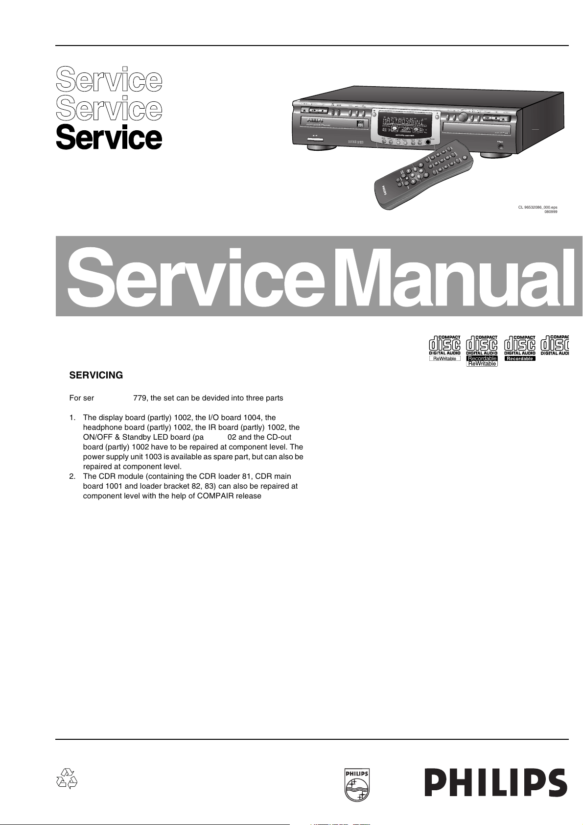
Compact disc recorder CDR779
/00
OPEN/CLOSE
OPEN/CLOSE
OPEN/CLOSE
PLAY/PAUSE
PLAY/PAUSE
PLAY/PAUSE
STOP
STOP
STOP
AUDIOCD RECORDABLE/REWRITABLE
AUDIOCD RECORDABLE/REWRITABLE
AUDIOCD RECORDABLE/REWRITABLE
ON/ OFF
REC
TYPE
RECORD
EXT
EXT
FINALIZE
ERASEFINALIZE
ERASE
SOURCE
SOURCE
R
e
c
o
r
d
a
b
l
e
DOUBLE SPEED
EASYJOG
EASYJOG
STORE/
STORE/
5
CDR
REM
REC
TIME
TRACK
TOTAL
REM
TRACK
3
MANUAL
I
I
SHUFFLE
4
56
CD
R
W
7
8
9
1011 12
RECORD
CHANGER
CDR775AUDIO CDRECORDER
DISPLAY
SCROLL
TIME
13
14
15
16
17
CD
RW
DJMODE
REPEAT
12
SYNC
DIGITAL
OPTICAL
ANALOG
PROG
5
CD
STEP
18
19
20
+
PROG
AB
SHUFFLE
ALL
REPEAT
SCAN
TRACK
PHONES
CANCEL/
CANCEL/
6
J
6
J
K
K
MENU
PLAY/PAUSE
MENU
PLAY/PAUSE
DELETE
DELETE
STOP
STOP
OPEN/CLOSE
AUDIOCD PLAYBACK
AUDIOCD PLAYBACK
IRSENSOR
OPEN/CLOSE
CL 96532086_000.eps
080999
ENTER
SERVICING
For servicing CDR779, the set can be devided into three parts
1. The display board (partly) 1002, the I/O board 1004, the
headphone board (partly) 1002, the IR board (partly) 1002, the
ON/OFF & Standby LED board (partly) 1002 and the CD-out
board (partly) 1002 have to be repaired at component level. The
power supply unit 1003 is available as spare part, but can also be
repaired at component level.
2. The CDR module (containing the CDR loader 81, CDR main
board 1001 and loader bracket 82, 83) can also be repaired at
component level with the help of COMPAIR release 1.6 and
higher. With this tool the diagnosing of the set can be done in an
interactive way. In the tool also the adjustment procedure has
been implemented. This is absolutely necessary in case the CDR
mainboard and/or (CDR loader) CDM is disconnected from the
matched production combination. Only designated workshops
can perform these repairs. Please send the complete set to the
designated workshop.
3. The CD module (containing the CD loader 131, CD mainboard
1005 and loader bracket 132) is a new module with VAL1250
loader assy but also a separate CDM and separate loader parts
will be available via service stock. The CD mainboard can be
repaired at component level.
Also available : Circuit Description “The Basics of Compact Disc
Recordable/Rewriteable”. Service codenumber 4822 725 25242.
Second line Repairmanual . Service codenumber 3104 125 40110.
©
Copyright 2000 Philips Consumer Electronics B.V. Eindhoven, The Netherlands.
All rights reserved. No part of this publication may be reproduced, stored in a
retrieval system or transmitted, in any form or by any means, electronic, mechanical,
photocopying, or otherwise without the prior permission of Philips.
Contents Page
1. Technical Specifications 2
2. Warning and Servicing Hints 4
3. User Instructions 7
Mechanical Instructions
4.
Wiring Diagram CDR 19
Wiring Diagram CD loader 20
Exploded View CDR 21
Exploded View CD loader 22
Dismantling Instructions 23
Block diagram, Circuit diagrams and PWB’s Diagram PWB
5.
Overall Blockdiagram 24
Display Board 25 26
IR / On/Off &Standby LED Board 27 27
Headphone / CD-out Board 28 28
I/O Board: EXT DAC (Diagram 1) 29 35
I/O Board: Cinch (Diagram 2) 30 35
I/O Board: Mic ADC (Diagram 3) 31 35
I/O Board: Power supply (Diagram 4) 32 35
I/O Board: DAC filter (Diagram 5) 33 35
I/O Board: DAC (Diagram 6) 34 35
Power Supply Unit 36 37
CD-Mainboard: Decoder & Servo (Diagram 1A) 38 42/43
CD-Mainboard: Servo drivers (Diagram 1B) 39 42/43
CD-Mainboard: Audio (Diagram 1C) 40 42/43
CD-Mainboard: Microprocessor (Diagram 2) 41 42/43
6. Diagnostic Software 45
7. Faultfinding Trees 49
8. Faultfinding Guide 55
9. List of Abbreviations 69
10. Partslist (mechanical and electrical) 75
Published by DP 0071 Service DPS Hasselt Printed in the Netherlands Subject to modification 5 3104 125 40190
Page 2

GB 2 CDR7791.
Technical Specifications CDR779
1. Technical Specifications CDR779
1.1 General
Mains voltage : all range version 84-
230V
Mains frequency : 50-60 Hz
Power consumption : 12W
DC output : +5V ± 10%, 50mA
max.
1.2 Input/output
1.2.1 Line output (CDR & CD)
Output level : 2Vrms at 0dB
Output resistance : 200Ω
1.2.2 Line input
Input sensitivity : 500mVrms
Input impedance : 50kΩ
Max. input voltage : 2.5Vrms
1.2.3 Digital output (CDR & CD)
Format : AES/EBU format
according IEC958
(consumer format)
Sampling frequency : 44.1kHz
Output resistance : 75Ω
1.2.4 Digital input
Format : AES/EBU format
according IEC958
(consumer format)
Sampling frequency : 32 to 48kHz
Input resistance : 75Ω
1.2.5 Optical input
Format : AES/EBU format
according IEC958
(consumer format)
Sampling frequency : 32 to 48kHz
1.3 Audio performance
1.3.1 Cinch analog output (CDR play-back)
Output voltage : 2Vrms ± 2dB. (0dB
digital).
Frequency range F.R. : 20Hz < F.R. <
20kHz.
Amplitude linearity : ± 0.15dB.
: typical.: ± 0.1dB.
Channel unbalance : <0.3dB at 1kHz.
:typical: ± 0.2dB.
Phase non-linearity : <0.2deg at 1kHz.
Outband attenuation : 50dB above 30kHz.
Channel separation : >100dB at 1kHz.
: typical: 110dB.
: >84dB from 20Hz.
until 20kHz.
: typical: >85dB.
S/N-ratio A-weighted : >99dB.
: typical: 100dB.
S/N-ratio unweightes : >97dB.
: typical: 98dB.
Dynamic range : > 94dB. at 1kHz.
: typical: 95dB.
THD+N : > 89dB from 20Hz.
until 20kHz.
: typical: 90dB.
1.3.2 Cinch analog input/output (monitor path CDR)
Measued with Audio precision system one.Input voltage is
2Vrms.
input voltage : 2Vrms ± 2dB. (0dB
digital).
Frequency range F.R. : 20Hz < F.R. <
20kHz.
Amplitude linearity : ± 0.2dB.
: typical.: ± 0.1dB.
Channel unbalance : < 0.2dB at 1kHz.
:typical: ± 0.15dB.
Input resistance : 25k(
Phase non-linearity : < 0.2deg at 1kHz.
Outband attenuation : 50dB above 30kHz.
Channel separation : > 90dB at 1kHz.
: typical: 100dB.
S/N-ratio A-weighted : > 87dB.
: typical: 93dB.
S/N-ratio unweighted : > 87dB.
: typical: 90dB.
Dynamic range : > 86dB. at 1kHz.
: typical: 90dB.
: > 86dB from 20Hz.
until 20kHz.
: typical: 90dB.
THD+N : > 86dB from 20Hz.
until 20kHz.
: typical: 87dB.
1.3.3 Cinch analog output (CD play-back)
Output voltage : 2Vrms ± 2dB. (0dB
digital).
Frequency range F.R. : 20Hz < F.R. <
20kHz.
Amplitude linearity : ± 0.3dB.
: typical.: ± 0.1dB.
Channel unbalance : <0.3dB at 1kHz.
:typical: ± 0.2dB.
Output resistance : 200(.
Phase non-linearity : <0.2deg at 1kHz.
Outband attenuation : 60dB above 30kHz.
Channel separation : >95dB at 1kHz.
: typical: 100dB.
: >90dB from 20Hz.
until 20kHz.
: typical: >93dB.
S/N-ratio A-weighted : >98dB.
: typical: 100dB.
S/N-ratio unweighted : >92dB.
: typical: 95dB.
Dynamic range : >92dB. at 1kHz.
: typical: 96dB.
: >90dB from 20Hz.
until 20kHz.
: typical: 96dB.
THD+N : >82dB from 20Hz.
until 20kHz.
: typical: 85dB.
Page 3

1.3.4 Headphone output (all functions)
Output voltage : 2Vrms (0dB)/16Ω
S/N : > 80dB
THD+N : > 78dB
Channel separation : > 60dB between
20Hz until 20kHz
1.4 Laser device
Material : GaAlAs
Wave length : between 780 and
800nm (at 25°C)
Laser output : 1mW max. during
reading, 20mW
max. during writing
Class : 3B
1.5 Dimensions and weight
Number and height of feet : 4x11mm foiled
Apparatus tray closed (WxDxH) : 435x305x75mm
(without feet)
Weight without packaging : 3.2kg
Weight with packaging : 4.2kg
Technical Specifications CDR779
GB 3CDR779 1.
Page 4
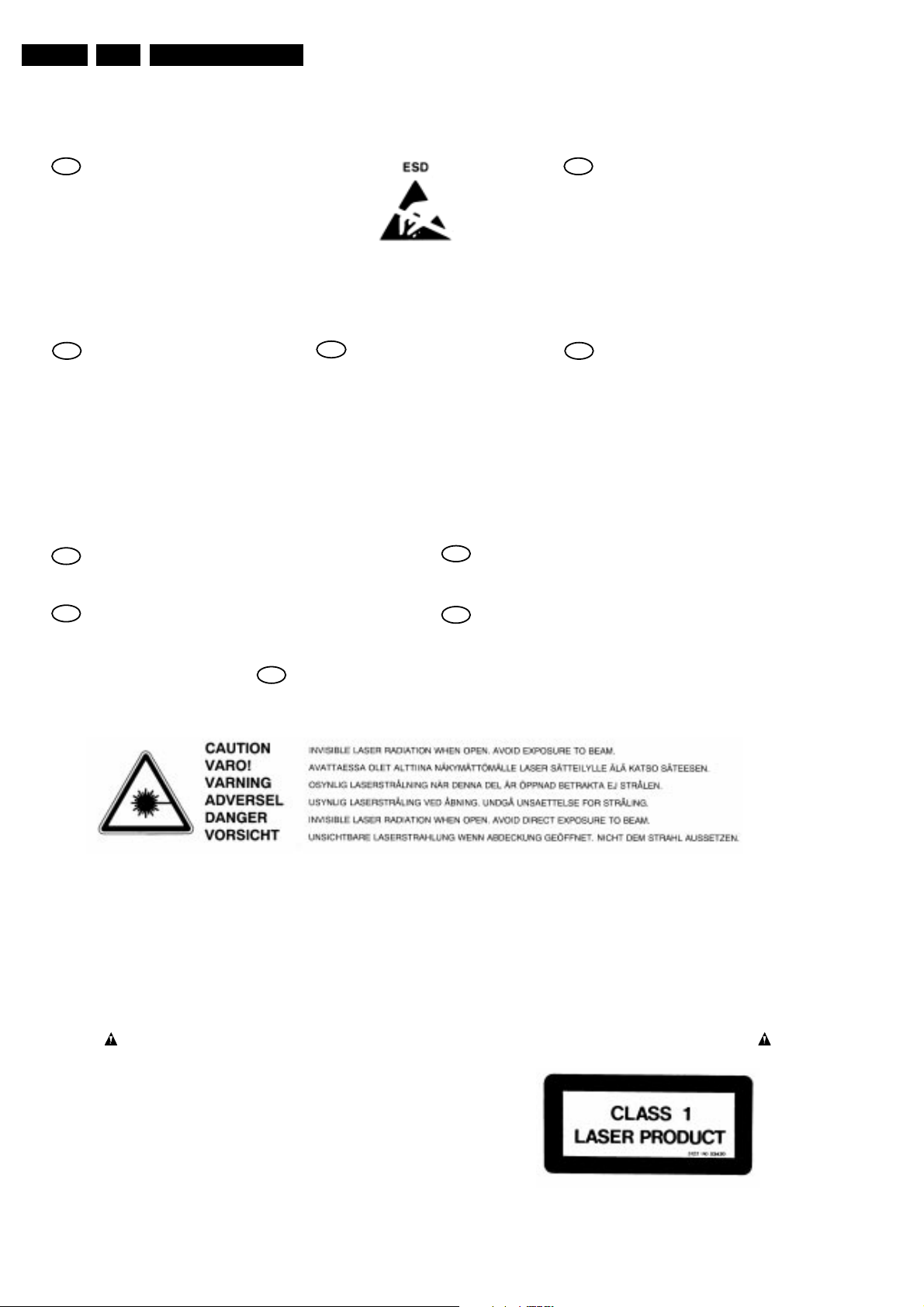
GB 4 CDR7792.
Warnings and Servicing Hints
2. Warnings and Servicing Hints
GB
WARNING
All ICs and many other semi-conductors are
susceptible to electrostatic discharges (ESD).
Careless handling during repair can reduce
life drastically.
When repairing, make sure that you are
connected with the same potential as the
mass of the set via a wrist wrap with
resistance.
Keep components and tools also at this
potential.
F
ATTENTION
Tous les IC et beaucoup d'autres semiconducteurs sont sensibles aux décharges
statiques (ESD).
Leur longévité pourrait être considérablement
écourtée par le fait qu'aucune précaution
n'est prise a leur manipulation.
Lors de réparations, s'assurer de bien être
relié au même potentiel que la masse de
l'appareil et enfiler le bracelet serti d'une
résistance de sécurité.
Veiller a ce que les composants ainsi que les
outils que l'on utilise soient également a ce
potentiel.
D
Alle IC und viele andere Halbleiter sind
empfindlich gegen elektrostatische
Entladungen (ESD).
Unsorgfältige Behandlung bei der Reparatur
kann die Lebensdauer drastisch vermindern.
Sorgen sie dafür, das Sie im Reparaturfall
über ein Pulsarmband mit Widerstand mit
dem Massepotential des Gerätes verbunden
sind.
Halten Sie Bauteile und Hilfsmittel ebenfalls
auf diesem Potential.
GB
Safety regulations require that the set be restored to its original condition
and that parts which are identical with those specified be used.
NL
Veiligheidsbepalingen vereisen, dat het apparaat in zijn oorspronkelijke
toestand wordt terug gebracht en dat onderdelen, identiek aan de
gespecifieerde worden toegepast.
F
Les normes de sécurité exigent que l'appareil soit remis a l'état d'origine et
que soient utilisées les pièces de rechange identiques à celles spécifiées.
WARNUNG
NL
Alle IC's en vele andere halfgeleiders zijn
gevoelig voor elektrostatische ontladingen
(ESD).
Onzorgvuldig behandelen tijdens reparatie
kan de levensduur drastisch doen
verminderen.
Zorg ervoor dat u tijdens reparatie via een
polsband met weerstand verbonden bent met
hetzelfde potentiaal als de massa van het
apparaat.
Houd componenten en hulpmiddelen ook op
ditzelfde potentiaal.
Tutti IC e parecchi semi-conduttori sono
sensibili alle scariche statiche (ESD).
La loro longevita potrebbe essere fortemente
ridatta in caso di non osservazione della piu
grande cauzione alla loro manipolazione.
Durante le riparazioni occorre quindi essere
collegato allo stesso potenziale che quello
della massa dell'apparecchio tramite un
braccialetto a resistenza.
Assicurarsi che i componenti e anche gli
utensili con quali si lavora siano anche a
questo potenziale.
WAARSCHUWING
I
AVVERTIMENTO
D
Bei jeder Reparatur sind die geltenden Sicherheitsvorschriften zu beachten.
Der Originalzustand des Gerats darf nicht verandert werden.
Fur Reparaturen sind Original-Ersatzteile zu verwenden.
I
Le norme di sicurezza esigono che l'apparecchio venga rimesso nelle
condizioni originali e che siano utilizzati pezzi di ricambiago idetici a quelli
specificati.
SHOCK, FIRE HAZARD SERVICE TEST:
CAUTION: After servicing this appliance and prior to returning to customer, measure the resistance between
either primary AC cord connector pins (with unit NOT connected to AC mains and its Power switch ON), and the
face or Front Panel of product and controls and chassis bottom,
Any resistance measurement less than 1 Megohms should cause unit to be repaired or corrected before AC
power is applied, and verified before return to user/customer.
Ref.UL Standard NO.1492.
NOTE ON SAFETY:
Symbol
: Fire or electrical shock hazard. Only original parts should be used to replace any part with symbol
Any other component substitution(other than original type), may increase risk or fire or electrical shock hazard.
“Pour votre sécurité, ces documents
doivent être utilisés par des
spécialistes agrées, seuls habilités à
réparer votre appareil en panne.”
CL 96532086_021.eps
080999
Page 5
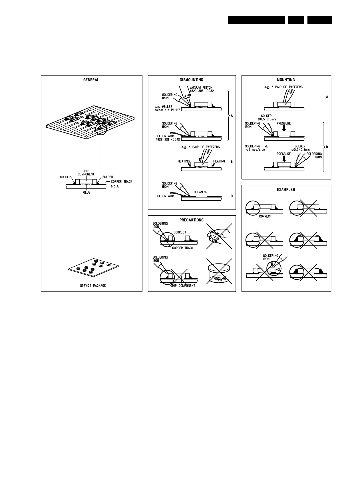
Warnings and Servicing Hints
SERVICING HINTS
In the set, chip components have been applied. For disassembly and assembly check the figure below.
GB 5CDR779 2.
CL 96532086_022.eps
080999
Page 6
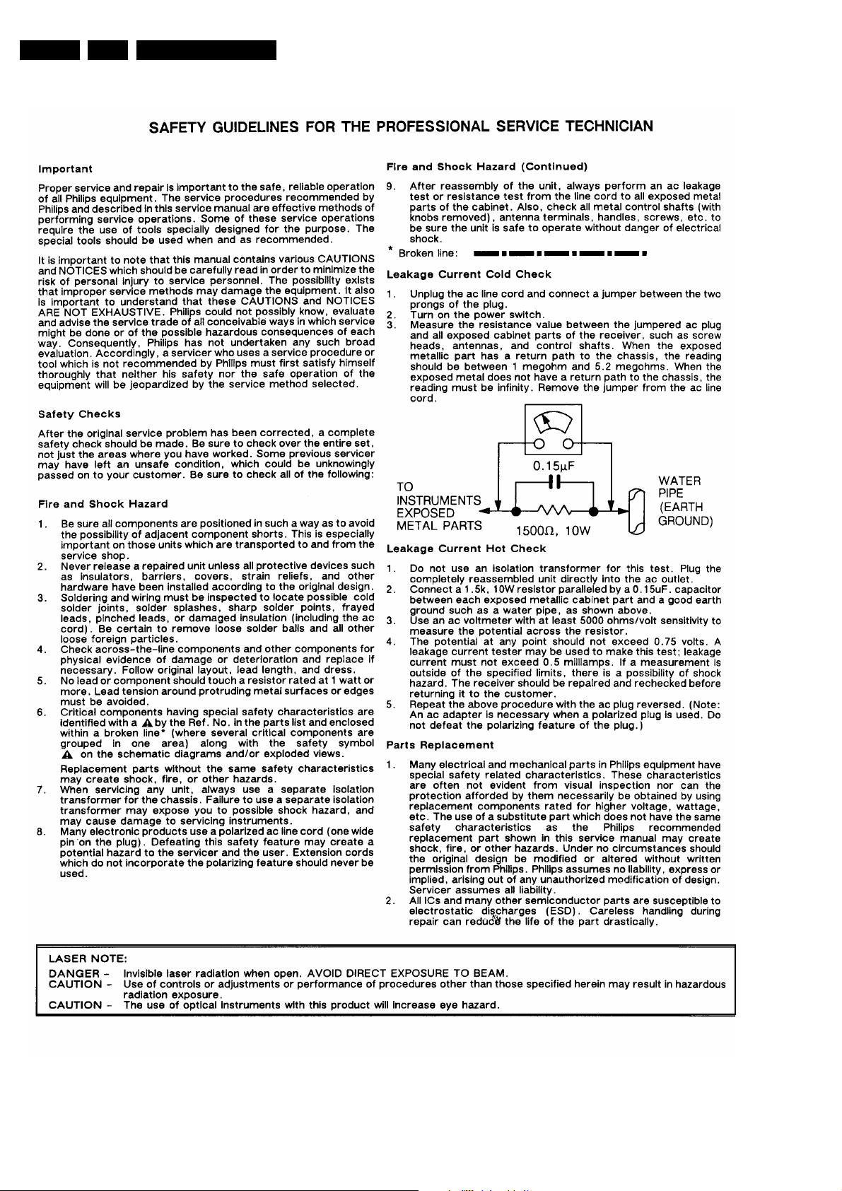
GB 6 CDR7792.
Warnings and Servicing Hints
CL 96532086_023.eps
080999
Page 7
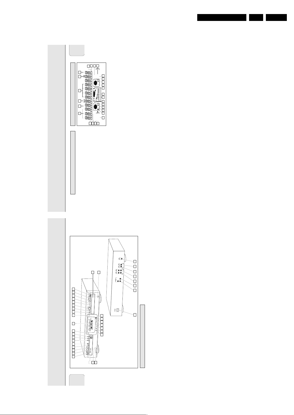
3. Directions for use
English
9
1 Connection to mains
2 ANALOG OUT ............connects CD player deck to the
line input of an amplifier (left and
right)
3 DIGITAL OUT CD ......connects CD player deck to the
digital coaxial input of e.g.
amplifier or recording device
4 ANALOG IN ................connects to the line output of an
amplifier (left and right)
5 ANALOG OUT CDR & CD
......................................connects to the line input of an
amplifier (left and right)
6 DIGITAL IN..................connects to the digital coaxial
output of an external CD player
7 DIGITAL OUT CDR & CD
......................................connects to the digital coaxial
input of e.g. amplifier or recording
device
8 OPTICAL IN ................connects to the digital optical
output of an external CD player
1 REM/REC TIME ..........remaining time/remaining
recording time/recording time
2 TRACK ........................track number
3
FE
..............................balance (lights during balance
adjustment)
4 TOTAL REM
TRACK TIME ..............total or remaining time of disc or
track
5
}
................................remote control active
6 STEP ............................indicates the number of tracks in a
program
7 Track bar ....................indicates:
- tracks on a disc or in a program
- track in play
8 + 20 ..............................disc or program contains more
than 20 tracks
9 PROG(ram) ..................flashes during programming/lights
in program mode
0 REPEAT TRACK/ALL..lights up when a track/ complete
disc (or program) is repeated
! SCAN ..........................lights up when the first 10
seconds of each track are played
@ SHUFFLE......................plays tracks in random order
#
s
..............................CD player deck selected
$
c
..............................CD inserted (a pre-recorded CD or
finalized CDR or CDRW disc)
% fRECORDg ............lights during recording from the
internal CD
^ L/R ; ; ........................record/play level bar. Indicates the
audio signal level
& j k ........................DJ mode selected
* iCHANGERh ........changer mode selected
( ; ..................................pause function active
) B ................................lights during play
¡ R(W) ............................unfinalized CDR(W) disc inserted
™ 0 ................................lights during recording
£ ANALOG ......................- analog input selected for
external recording
- analog recording
≤ OPTICAL I ..................optical input I selected for external
recording
∞ DIGITAL I ....................digital input I selected for external
recording
§ SYNC ..........................automatic or synchronised start of
external recording
≥ MANUAL ....................manual operation of external
recording
REM
TRACK
REC
TIME
DIGITAL
OPTICAL
ANALOG
PROG
SHUFFLE
REPEAT
SCAN
I
I
CD
RW
CHANGER
SYNC MANUAL
RECORD
REMTOTAL
ALL
TRACK
TIME STEPTRACK
CD
RW
123456789
10 11 12 13 14 15 16 17 18 19 20 +
1 2 3 4 5
10
1617
19202122
23
24
272625
12131415
6
7
8
9
11
18
DISPLAY indicationsConnections at the back
CONTROLS AND CONNECTIONS DISPLAY
Directions for use
GB 7CDR779 3.
L
A
R
C
D
N
I
C
I
T
P
O
T
R
D
D
U
L
C
C
O
A
T
GI
I
R
D
N
D
I
C
L
R
R
D
D
C
C
D
C
L
R
D
C
L
R
T
U
G
O
O
L
A
N
A
N
I
L
A
T
T
I
U
G
I
O
D
G
T
O
U
L
O
A
N
A
- recording level control (recording)
- selects settings (menu on)
6
- programs track numbers
- enters Menu mode
- deletes text in Menu mode
menu
- returns to a higher level in the
control
and CD player deck
5432
(rotate) Program mode)
ENTER..........................- plays selected tracks
(push) - selects settings in Menu mode
* STORE/MENU ............- stores Menu settings
( CANCEL/DELETE ......- deletes tracks from a program
≤ IR sensor ....................receives signals from the remote
∞ PHONES ......................socket for headphones
§ DJ MODE....................separate play of CD recorder deck
≥ REPEAT........................repeats play (All, program or track)
& ¡ EASY JOG ™ ........- previous/next track (Play and
1 87
the recorder is in Standby mode,
any key press will activate the CD
recorder)
2 Standby indicator
3 Disc tray
4 OPEN/CLOSE /..........opens/closes disc tray
5 PLAY/PAUSE 2; ......starts play/interrupts play or
recording
6 STOP 9........................stops/clears a program
7 REC(ord) TYPE ............selects recording modes
8 RECORD ......................starts recording, finalizing, erasing
9 FINALIZE ....................selects finalize mode
0 ERASE ..........................selects erasing mode (disc or track)
! EXT SOURCE ..............selects external input source
display/keys
@ CDR ............................selects CD recorder deck
Controls on the front
CD recorder
1 ON/OFF ........................turns the CD recorder ON or OFF (if
14 15 16 17 18 19 20 21 22
7 8
4 65 9 10 11 12 13
CONTROLS AND CONNECTIONS
E
C
T
R
X
E
OU
S
E
S
A
R
E
E
Z
I
L
A
IN
F
D
R
O
REC
C
PE
Y
RE
T
P
P
O
O
T
T
S
S
E
E
S
S
U
U
A
A
P
P
/
/
Y
Y
A
A
L
L
P
P
E
SE
S
O
O
L
L
C
C
/
/
N
N
E
E
P
P
O
O
/
L
E
E
T
C
E
L
N
E
A
D
C
/
E
U
R
N
O
E
T
M
S
R
E
T
N
E
G
O
J
Y
S
A
E
CD
L
B
-
P
L
E
A
A
T
+
S
E
L
F
20
F
G
U
O
9
H
R
P
S
181
D
17
E
C
M
I
T
16
K
5
C
A
R
T
41
R
M
D
E
E
R
131
R
G
O
N
C
2
L
A
1
A
H
RE
T
C
O
T
11
10
9
8
K
C
A
7
D
R
C
T
6
E
M
I
5
T
L
A
4
C
U
E
N
R
3
A
I
I
L
M
L
2
A
A
M
C
C
T
I
I
E
N
T
R
G
1
I
P
Y
D
O
S
CDR
e
l
b
a
d
r
o
c
e
R
E
E
L
L
B
B
TA
TA
I
I
R
R
EW
EW
R
R
/
/
LE
LE
B
B
A
A
D
D
R
R
O
O
EC
EC
R
R
D
D
C
C
O
O
I
I
D
D
U
U
A
A
3
23
24
R
O
S
N
E
D PLAYBACK
IR S
C
IO
AUD
ES
N
O
PH
K
C
A
R
T
E
T
A
D
N
E
O
A
P
E
C
R
S
M
J
D
T
W
A
E
R
P
E
R
RDER
O
L
L
O
R
C
S
Y
A
L
P
IS
D
R 779 AUDIO CD REC
E
W
L
R
CD
F
F
U
H
S
G
G
O
O
L
R
A
P
N
A
D
E
E
P
S
E
L
B
U
O
D
F
F
/ O
N
O
1
2
26 25
3031 29 2728
• SCROLL ........................activates scrolling of text over the
CD player
display (once)
ª DISPLAY ......................selects display information,
$ CD ..............................selects CD player deck
permanent text scrolling and time
random order
º SHUFFLE ......................plays CD(RW) or program in
display/keys
) PLAY/PAUSE 2; ......starts play/interrupts play
¡ STOP 9........................stops/clears a program
⁄ PROG(ram) ..................opens/closes program memory
™ OPEN/CLOSE /..........opens/closes disc tray
£ Disc tray
Note: Unless stated otherwise, all controls are on the front of
the CD recorder. When provided on the remote control,
you can also use the corresponding buttons, after
General
selecting the CD recorder deck or CD player deck by
# Display ..........................information screen
pressing CDR or CD.
- cursor control in Menu/Prog.
% Q ............................- searches backward
review mode
- cursor control in Menu/Prog.
^ R ............................- searches forward
review mode
8
English
Page 8
GB 8 CDR7793.
English
11
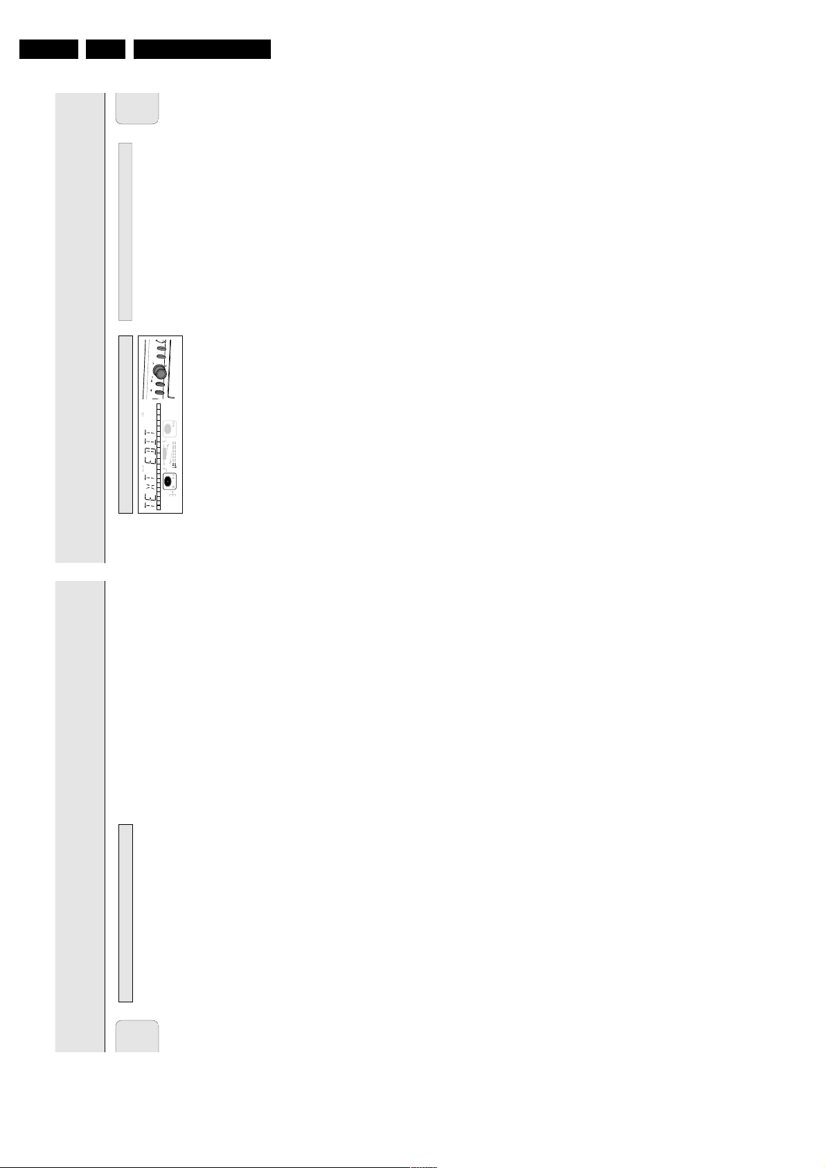
Menu messages
NO TRACKS ....................when attempting to edit text for a
disc which has no tracks
TEXT EDIT ....................when entering Text Edit mode
ALBUM ARTIST ............when editing or erasing an artist
name
ALBUM TITLE ..............when editing or erasing a title
ARTIST TR X ................when editing or erasing an artist
name per track
TITLE TR X ..................when editing or erasing a title per
track
TEXT ERASE ..................when entering Text Erase mode
ALL TEXT ......................when entering All Text mode
ERASE OK ......................when confirmation for erasing has
to be given with ENTER key
ERASE ALL OK ............when confirmation for erasing has
to be given with ENTER key
ERASE MEMORY ............when waiting for confirmation
when erasing a disc
MEMORY VIEW ..............when selecting text review per
unfinalized disc in memory
MEMORY EMPTY ............when REVIEW is selected while no
text is in memory
AUTO TRACK ..................when selecting auto track
increment ON or OFF
ON ......................................auto track increment on
OFF ....................................auto track increment off
SET BALANCE ..............when selecting BALANCE
NO TEXT ..........................no text stored for disc
For playback on the CD recorder (and/or CD player deck) the
following outputs are present:
- Digital coaxial output (CD & CDR);
- Analog output (CD & CDR).
We advise you to connect these to the TAPE or CDR input on
your amplifier.
For external recording the following inputs are present:
- Digital optical input;
- Digital coaxial input;
- Analog input.
For playback of CD player deck separately (DJ mode) from the
CD recorder the following outputs are present:
- Digital coaxial output (CD);
- Analog output (CD).
We advise you to connect these to the CD input on your
amplifier.
The connections you make will depend upon the possibilities
your audio equipment offers. Please refer to the user manuals
for your other audio equipment first.
Digital recordings (optical or coaxial) give the best
performance in audio and usability (e.g. auto-track).
(The digital optical connection is less sensitive to external
disturbances).
If your equipment does not offer digital connections, the high
quality Analog-Digital-Convertor of your CD recorder will
ensure very good audio performance when recordings are
made from the analog input.
Playback via the digital coaxial output of the CD recorder
gives the best audio performance.
If your equipment does not offer digital connections, the high
quality Digital-Analog-Convertor of the CD recorder ensures a
very good sound quality via the analog output.
We advise you to always establish both digital and analog
connections. In this way you can always make analog
recordings when digital recording is not possible.
We have described the most common ways of connecting the
CD recorder. If you still have difficulties with the connections
you can always contact the Philips Consumer Service desk in
your country.
Connections general
E
A
SY
JO
G
S
T
O
R
E
/
M
E
N
U
C
A
N
C
E
L
/
D
E
L
E
T
E
E
N
TER
REM
TRACK
REC
TIME
DIGITAL
OPTICAL
ANALOG
PROG
SHUFFLE
REPEAT
SCAN
I
I
CD
RW
CHANGER
SYNC MANUAL
RECORD
REMTOTAL
ALL
TRACK
TIME STEPTRACK
CD
RW
MENU messages - See Menu mode
DISPLAY INSTALLATION
English
10
Messages, as listed and explained here, may appear on the
display for your guidance.
General
READING..........................reading disc information
OPEN..................................during tray opening
CLOSE ..............................during tray closing
NO DISC ..........................no disc inserted, disc unreadable
or disc inserted upside down
PROG FULL ....................program full
INSERT DISC ..............insert disc or insert disc in correct
way
WRONG DISC/ ................inserted disc is not an audio CD
USE AUDIO CD
UNFINALIZED ..............unfinalized CDR(W) disc
MEMORY XXù ............indicates the amount of text
memory used for unfinalized discs
Recording
WAIT..................................- when STOP 9 is pressed during
recording
- when STOP 9 is pressed during
recording the first 4 seconds of a
track
UPDATE ..........................updating disc contents
DISC FULL ....................no more recording possible
DIGITAL 1 ....................digital coaxial input 1 selected
OPTICAL ........................digital optical input selected
ANALOG ............................analog input selected
COPY PROTECT ............no digital recording can be made
of the external source
NOTFINALIZED ............when opening the tray with an
unfinalized disc inserted
(CD recorder)
RECORD FAST ..............high speed recording selected
REC LISTEN ..................listen speed recording selected
MAKE CD ..........................high speed recording of a
complete disc and Auto Finalize
function selected
REC EXT DISC ............synchronised start of recording
from external source selected
REC EXT MAN ................manual start of recording from
external source selected
_XX DB ............................level is being adjusted
DOES NOT FIT ............time left on CDR(W) disc is not
enough for proposed recording
ANALOG REC ..................copy prohibited track found during
recording. Track will be copied
analog (Copy Protection Regulations)
ERASE TRACK ..............when erasing one or more tracks
ERASE DISC ..................when erasing a disc
FINALIZE CD ..............when finalizing a disc
FINALIZED ....................when trying to finalize an already
finalized disc
CHECK INPUT ..............when RECORD is pressed while no
digital source is detected
XX XX ERASE ................time countdown when erasing a
track or a disc
XX XX FINAL ................time countdown when finalizing a
disc
PRESS RECORD ............to start manual recording,
finalizing or erasing
START SOURCE ............to start synchronised recording
from a source (e.g. CD player)
FINALIZED CD ............when trying to record on a
finalized CDR or a prerecorded CD
UNFINALIZE/ ................when trying to record on a
PRESS ENTER finalized CDRW
PROF SOURCE ..............when a professional source is
connected
REC TEXT ......................when reading CD text from source
disc for recording
TEXT PROTECT ............when CD text of source disc is
subjected to copy protection (CD
text will not be recorded)
Play
CHANGER MODE ............CD changer-mode selected
DJ MODE ..........................DJ- mode selected when recording
keys are pressed in DJ-mode
PROGRAM..........................program mode selected
ALBUM TITLE ..............will be followed by album title
TRACK TITLE ..............will be followed by track title
ALBUM ARTIST ............will be followed by artist name
TRACK ARTIST ............will be followed by track artist
name
Others
NO AUDIO TR ................when the recorder enters a data
track during recording
FINALIZE CD ..............laser power calibration performed
96 times, finalize disc needed
INITIALIZING ............during laser power calibration for
unfinalized discs
DISC RECOVER ............during disc recovering after power
failure
OPC ERROR ....................OPC failure during OPC procedure
(OPC = Optimum Power
Calibration)
RECORD ERROR ............recording error in menu mode
DISC ERROR ..................when trying to record on or finalize
a recovered disc
MEMORY FULL/ ..............when text memory is full. To add a
FINALIZE CD CD to the list, first finalize or
erase another disc from the list
NOT POSSIBLE ............when trying to erase a CDR
DISPLAY messages
DISPLAY
Directions for use
Page 9
Directions for use
English
13
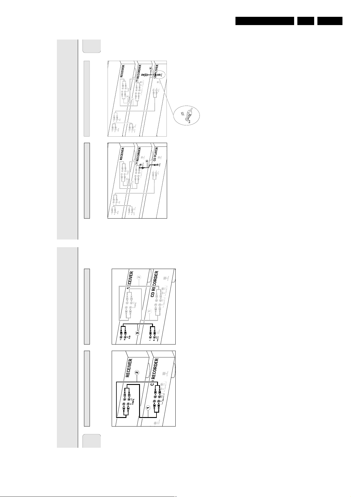
This connection is only required if you want to make
recordings from an external CD player with a digital coaxial
output.
Use the digital coaxial cable supplied.
1 For external recording, connect the cable 4 between the
DIGITAL IN-socket on the CD recorder and the DIGITAL OUT-
socket of an external CD player.
Note: Your CD recorder is equipped with a digital coaxial
output (common output for CD recorder & CD player
deck). This output can be used for digital playback.
This connection is only required if you want to make
recordings from an external CD player with a digital optical
output.
When connecting the Digital
Optical cable, make sure it
is fully inserted until
there is a click.
1 Remove the dust caps from the digital optical connection.
(We recommend you save the cap.)
2 For external recording, connect a fibre-optic cable 5
between the digital optical input of the CD recorder and the
digital-optical output of an external CD player.
Note: For playback, the digital coaxial outputs or analog
outputs of the CD Player and CD recorder should be
connected to an amplifier.
Digital optical connections CD recorderDigital coaxial connections CD recorder
INSTALLATION
GB 9CDR779 3.
INSTALLATION
Analog connections CD player deckAnalog connections CD recorder & CD player
English
third cable 3 (not supplied) between the ANALOG OUT
sockets of the CD recorder and the input sockets of an
amplifier e.g. CD, or AUX.
(Connect the red plugs to the R sockets, and the white plugs
R sockets, and the white plugs to the L sockets.
to the L socket.)
sockets on the CD recorder and the CDR LINE- or TAPE OUT-
sockets of an amplifier.
1 For recording, connect cable 1 between the ANALOG IN-
This connection is only required if you want to playback on
the CD player deck seperately from the CD recorder deck. This
will be the case in DJ-mode.
).
2
is only required if you want to make recordings from
1
Cable
an external analog source.
This connection must be made for playback on the CD
recorder deck as well as the CD player deck (cable
1 For separate playback on the CD player deck, connect a
Use the audio cables supplied. Connect the red plugs to the
Note:
Note: For recording directly from a CD player, the analog input
- Never use the PHONO input.
of the CD recorder should be connected to the analog
output for the CD player deck. This output can be used for
- Your CD recorder/player is equipped with a digital coaxial
output of the CD player.
digital playback.
sockets on the CD recorder and the input sockets of an
2 For playback, connect cable 2 between the ANALOG OUT-
amplifier e.g. TAPE IN, CDR or AUX.
Note: Never use the PHONO input.
12
Page 10
GB 10 CDR7793.
English
15
STANDBY
B
....................switches to Standby/On
SCAN ................................plays the first 10 seconds of each
track
SHUFFLE............................plays CD(RW) or program in
random order
REPEAT..............................repeat play
Number/alphabet keys 0 - 9
......................................- selects a track by number
- selects character for text input
TRACK INCR(ement) ........increases track numbers during
recording
SPACE................................inserts a space character during
text input
SCROLL..............................activates scrolling of text over the
display
CDR ....................................selects CD recorder deck
CD ......................................selects CD player deck
2 ......................................starts CD(RW) play
O ......................................- previous track (Play and Program
mode)
- cursor control in Menu/Prog.
review mode
P ......................................- next track (Play and Program
mode)
- cursor control in Menu/Prog.
review mode
9 ......................................stops CD(RW) and clears a
program
Q....................................searches backward
R....................................searches forward
; ......................................interrupts CD(RW) play/recording
MENU/STORE ..................- enters Menu mode
- stores Menu settings
PROG.(ram) ........................opens/closes program memory
ENTER................................- selects settings in Menu mode
- programs track numbers
- starts playback of selected track
CANCEL ............................- deletes tracks from a program
- deletes text in Menu mode
- returns to a higher level in the
menu
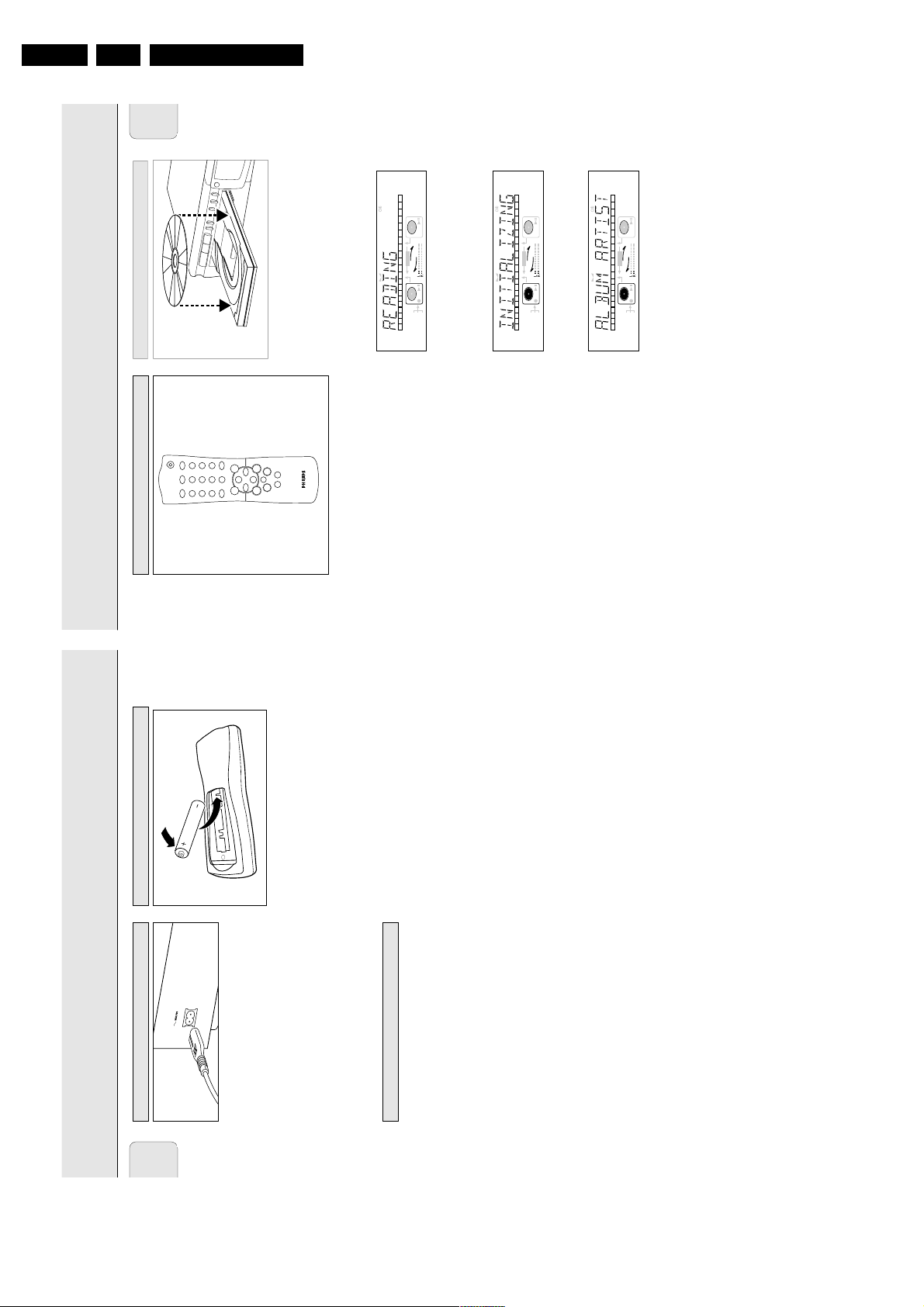
1 Press OPEN/CLOSE to open the disc tray.
➜ OPEN lights up.
2 Insert a CD, CDR or CDRW in the appropriate recess in the
tray, label side up.
3 Press OPEN/CLOSE to close the tray (see also Playing a CD).
➜ CLOSE lights up, followed by READING and the
display will show the type of disc you inserted.
•If you insert a blank or partly-recorded CDR or unfinalized
CDRW, the CD recorder will calibrate the disc for optimum
recording. During this process the display will first show
INITIALIZING and then the number of audio tracks.
Calibration can take up to 25 seconds.
• If a CDR(W) is finalized it will show
CD
on the display.
• If CD-text is available the TITLE/ARTIST will scroll by.
Note:
- Only Audio CDs will be accepted. If a non-audio disc is
inserted, the display shows
WRONG DISC/
USE AUDIO CD
.
- Reading an unfinalized disc in the CD recorder deck could
take approximately 1 minute.
- For recording it is important that the blank disc is completely
free from dust particles or scratches. (see maintenance).
REM
TRACK
REC
TIME
DIGITAL
OPTICAL
ANALOG
PROG
SHUFFLE
REPEAT
SCAN
I
I
CD
RW
CHANGER
SYNC MANUAL
RECORD
REMTOTAL
ALL
TRACK
TIME STEPTRACK
CD
RW
123456789
10 11 12 13 14 15
REM
TRACK
REC
TIME
DIGITAL
OPTICAL
ANALOG
PROG
SHUFFLE
REPEAT
SCAN
I
I
CD
RW
CHANGER
SYNC MANUAL
RECORD
REMTOTAL
ALL
TRACK
TIME STEPTRACK
CD
RW
REM
TRACK
REC
TIME
DIGITAL
OPTICAL
ANALOG
PROG
SHUFFLE
REPEAT
SCAN
I
I
CD
RW
CHANGER
SYNC MANUAL
RECORD
REMTOTAL
ALL
TRACK
TIME STEPTRACK
CD
RW
O
N
/
O
F
F
C
D
R
F
I
N
A
L
I
Z
E
O
P
E
N
/C
L
O
S
E
P
L
A
Y
/P
A
U
S
E
S
T
O
P
R
E
C
T
Y
P
E
R
E
C
O
R
D
ER
A
S
E
E
X
T
S
O
U
R
C
E
D
I
R
E
C
T
L
I
N
E
R
EC
O
R
D
I
N
G
D
OU
BLE SPEED
Inserting discs
SCAN
ABC DEF GHI
JKL MN OPQ
RST UVW XYZ
TRACK INCR.
MENU/
STORE
PROG.
ENTER CANCEL
CDR
2
9
;
KJ
56
CD
SPACE SCROLL
SHUFFLE REPEAT
1
2
3
456
7
8
9
0
Remote control commands
REMOTE CONTROL
English
14
1 Plug the power cord supplied into the MAINS connector on
the CD recorder, then into a mains socket.
2 Press ON/OFF.
➜ The CD recorder will switch on.
3 The recorder switches automatically to active mode.
Note: When the CD recorder is in the ‘OFF’ position, it is still
consuming some power. If you wish to disconnect your
player completely from the mains, withdraw the plug
from the AC outlet.
- Place the CD recorder on a solid, vibration free surface.
- Do not place the CD recorder near a source of heat or in
direct sunlight.
- Do not use the CD recorder under extremely damp
conditions.
- If the CD recorder is placed in a cabinet, make sure that a
2.5 cm space remains free on all sides of the CD recorder
for proper ventilation.
Important:
- Do not put the CD recorder on top of other equipment that
heats up the CD recorder (e.g. receiver or amplifier).
1 Open the battery compartment cover.
2 Insert 2 batteries (“AA”, LR-6 or UM-3; as supplied) as
shown.
3 Replace the cover.
Note: We recommend you use 2 batteries of the same type
and condition.
Batteries contain chemical substances, so they should
be disposed of properly.
Inserting batteries in the remote control
Setup recommendations
Power supply
INSTALLATION
Directions for use
Page 11
Directions for use
English
17
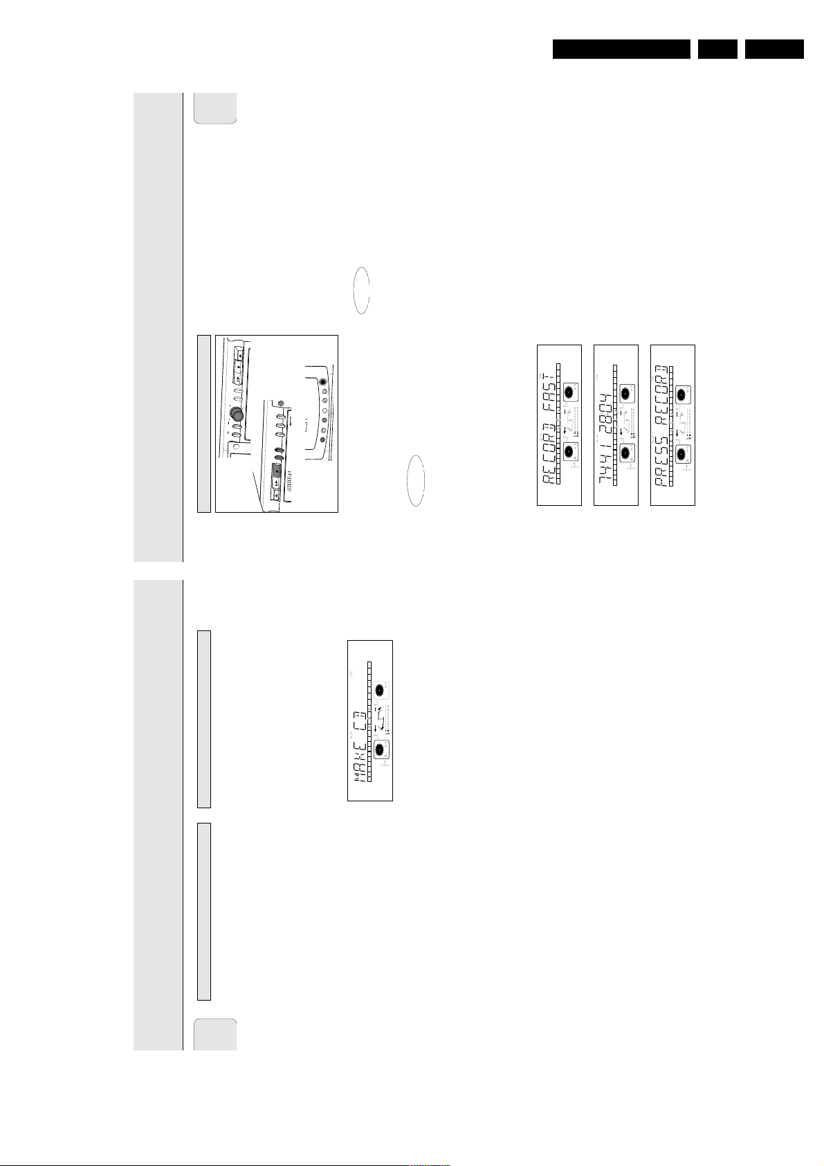
During high speed recording the sound is not audible.
Preparing for high speed recording
1 Make sure that the recording disc is absolutely free of
scratches and dust particles.
2 Press REC TYPE to choose the type of recording:
once: to select ‘RECORD FAST’ if you wish to make a
fast recording of a disc or programmed tracks;
three times: to select ‘MAKE CD’ if you wish to make a
fast recording of a disc or programmed tracks
and to automatically finalize the recording.
➜ The display first shows the selection.
The fRECORDg label starts blinking. After 3 seconds
the display shows the remaining CDR(W) recording time
on the left and total time of source on the right. (every 2
seconds PRESS RECORD is displayed.) The left
selection indicator is lit.
•If DOES NOT FIT appears on the display, there is not
enough recording space left on the CDR(W) disc.
You can press RECORD: only complete tracks that still fit on
the CDR(W) will recorded.orYou can press PROG to select one or more tracks for
recording (see programming):
- rotate the EASY JOG/ENTER key to the required track
number, then press the key (or ENTER on the remote
control)
or
- directly select the track number via the 10-keypad on the
remote control then press the ENTER key to confirm your
selection and go to the next step.
Start high speed recording
1 Press RECORD to start recording.
➜ WAIT lights up. The display shows the total remaining
time for the selected recording. High speed recording
starts. fRECORDg lights continuously.
•To check the track number and track time, press DISPLAY.
This can be done during recording.
•Recording will stop automatically.
Note: Copy prohibited tracks will be copied analog.
ANALOG
REC
is displayed.
2 To stop recording manually, press STOP.
➜ UPDATE lights up, fRECORDg goes out and
recording stops. (Minimal track length must be 4 seconds
otherwise silence will be added to the track.)
•If STOP was pressed within 3 seconds after RECORD, no
recording will take place.
After recording, the display shows UPDATE for several
seconds. The Total time indications can differ slightly.
However, no music information is lost.
Note: In this Recording mode, the Pause function is not
operative.
Important:
If you want to play the recorded CDR disc on any
regular CD player, it must first be finalized. See
finalizing discs.
Finalized CDRW discs play only on CDRW compatible
CD players.
REM
TRACK
REC
TIME
DIGITAL
OPTICAL
ANALOG
PROG
SHUFFLE
REPEAT
SCAN
I
I
CD
RW
CHANGER
SYNC MANUAL
REMTOTAL
ALL
TRACK
TIME STEPTRACK
CD
RW
RECORD
REM
TRACK
REC
TIME
DIGITAL
OPTICAL
ANALOG
PROG
SHUFFLE
REPEAT
SCAN
I
I
CD
RW
CHANGER
SYNC MANUAL
REMTOTAL
ALL
TRACK
TIME STEPTRACK
CD
RW
RECORD
REM
TRACK
REC
TIME
DIGITAL
OPTICAL
ANALOG
PROG
SHUFFLE
REPEAT
SCAN
I
I
CD
RW
CHANGER
SYNC MANUAL
REMTOTAL
ALL
TRACK
TIME STEPTRACK
CD
RW
RECORD
O
P
E
N
/
C
L
O
S
E
P
L
A
Y
/
P
A
U
S
E
S
T
O
P
R
E
C
T
Y
P
E
O
P
E
N
/
C
L
O
S
E
P
L
A
Y
/
P
A
U
S
E
S
T
O
P
E
X
T
S
O
U
R
C
E
E
RA
S
EF
I
NA
L
I
Z
E
C
D
R
R
E
C
O
R
D
EA
S
Y
J
O
G
ST
ORE
/
M
E
NU
C
A
N
CE
L/
D
E
LE
T
E
C
D
E
N
T
E
R
P
H
O
N
E
S
DISPLAY
SCROLL
DJ MODE
REPEAT
SHUFFLE
PROG
C
D
R
7
7
9
A
U
D
I
O
C
D
R
E
C
O
R
D
E
R
A
N
A
L
O
G
R
W
High speed recording from internal CD player
RECORDING
GB 11CDR779 3.
Recording modesRemarks about recording
RECORDING
English
Your recorder offers several recording modes.
You will soon discover how easy it is to make your own CDs.
For recording from internal CD-deck:
Nevertheless, it is advisable to use a CDRW disc for your first
try.
We will describe:
- RECORD FAST (high speed digital recording) - fast recording
- Recording from internal CD player deck: high speed or
of a disc or programmed tracks.
listen mode.
- Recording from an external CD player deck: syncronized
- REC LISTEN (normal speed digital recording) - listening to a
start with CD player or manual start. (analog or digital).
recording while making it.
- MAKE CD (high speed digital recording and auto-finalize) -
•If the disc is a CDRW and is already finalized you must
fast recording of a disc or programmed tracks. Recording
will be finalized automatically.
unfinalize it first.
disc!
Warning: No more recording possible after finalizing CDR
CDRWs.
•The recording procedure is the same for CDRs and
TIME STEPTRACK
REMTOTAL
TRACK
TIME
REC
REM
automatically search for the end of the last track, so that
•If the disc already contains recordings, the CD recorder will
PROG
RECORD
SYNC MANUAL
recording can start from there.
ALL
SHUFFLE
REPEAT
CD
RW
CHANGER
CD
RW
I
I
DIGITAL
OPTICAL
TRACK
SCAN
ANALOG
•CD text can be added to a recording in Stop mode and
For recording from external sources:
during recording.
appears, the track
ANALOG REC
will be recorded as analog, at normal speed. All other
- REC EXT DISC (automatic start of recording) - to make an
automatic recording of an external source simply by starting
the source.
recording from an external source.
- REC EXT MAN (manual start of recording) - to start a manual
Some remarks on recording:
- During high speed recording, the original recording quality
will be maintained.
automatically be increased during recording.
- When Auto track is on (default setting), track numbers will
- By programming tracks first, a compilation can be recorded.
- If a finalized CD recordable disc is inserted in the CD
recorder, FINALIZED CD will be displayed when REC
TYPE is pressed. Recording is not possible.
- If a finalized CD rewritable disc is inserted in the CD
displayed when the REC TYPE is pressed. If ENTER is
recorder, UNFINALIZE and PRESS ENTER will be
pressed, the disc will be unfinalized.
Note: If during recording
tracks will be copied normally (at double speed).
REC EXT
(Text information is not available on the output of the CD
player.)
•CD text can not be recorded from an external CD player.
internal CD player deck. (If not subjected to copy
protection.) This may take up to 2 minutes.
the disc, otherwise you will not be able to enter record
standby mode. DISC FULL then lights up.
•The CD recorder deck is able to record CD text from the
•There must be at least 7 seconds of recording time left on
•If the display indicates COPY PROTECT, no digital
recording can be made of the source material. Recording
will not start.
allows digital recording under specific conditions:
•The Serial Copy Management System (SCMS) only
- This means that it is not possible to make a digital copy
from a digital copy.
- Analog recording is always possible!
- The number of recordings from the original is unlimited.
•A maximum of 99 tracks can be recorded on a disc.
Minimum allowable track length is 4 seconds.
•Recordings from DAT or DCC players will not always stop
automatically.
Important:
If you want to play the recorded CDR disc on any
regular CD player, it must first be finalized. See
finalizing discs.
Finalized CDRW discs play only on CDRW compatible
CD players.
For recording from CD changers always use
.
DISC
16
Page 12
GB 12 CDR7793.
English
19
Important:
- Recording from CD-changers should always be started in the
Auto-Start mode.
- Only make analog recordings when digital recording is not
possible.
Preparing for manual recording
1 Make sure the disc is absolutely free of scratches and dust
particles.
2 Press EXT(ernal) SOURCE repeatedly until (depending on the
connection used):
➜ DIGITAL I, OPTICAL I or ANALOG lights up and
DIGITAL 1, OPTICAL or ANALOG appears on the
display.
•When Auto Track is On (default setting), track numbers will
automatically be increased during recording.
•To switch off the Auto Track function you have to enter
Menu mode.
If you wish to increase track numbers manually, press
TRACK INCR(ement) on the remote control. For further
instructions see Menu mode.
ON (Auto): The track increments are automatically taken over
from the digital source material or after 2.7 seconds
silence during analog recording.
OFF (Manual): While recording track numbers can be
incremented manually by pressing TRACK INCR(ement) on
the remote control. (Minimum track length is 4 sec.) (This
can also be done in Auto track ON mode.)
• Track numbers cannot be changed after recording.
Note: Auto track works only with Consumer Sources with a
digital output signal according to the IEC 958 (consumer
part) audio standard.
3 With the recorder stopped, press REC TYPE five times to
enter the Manual Record standby mode.
➜ Display shows REC EXT MAN followed by WAIT.
After a few seconds PRESS RECORD followed by the
remaining time and track number appear on the display.
4 Play the source first to set the optimal recording level on
the CD recorder.
5 Rotate the EASY JOG/ENTER key until, on the Record/Play
Level bar, all the blue segments are alight, but the red
segments do not light continuously during the loudest
passages.
➜ Display shows _XX DB (Decibel, e.g. -3DB).
6 Stop the source.
Start manual recording
1 To start recording, press RECORD on the CD recorder and
immediately start the source (from Pause or Stop-mode).
➜ d lights continuously. The track number and recording
time left appear on the display.
•If CHECK INPUT message also flashes, the digital
connection is incorrect.
•To record a 3-second silence at the start of a track, press
PAUSE on the CD recorder before starting the source.
• To check the total remaining recording time, press DISPLAY on
the CD recorder. (This can also be done during the recording.)
2 To stop recording, press STOP on the CD recorder.
➜ UPDATE lights up and d goes out.
• If STOP was pressed within 3 seconds after RECORD, no
recording will take place.
• To interrupt recording, press PAUSE on the CD recorder.
d starts to flash. Press PAUSE again to restart recording.
( A new track will always be made.)
After recording the display will show UPDATE for several
seconds.
Note: Recordings made analogously will stop after 20 seconds
silence. With
AUTO TRACK OFF
, the auto stop mode is
disabled.
Important:
If you want to play the recorded CDR disc on any
regular CD player, it must first be finalized. See
finalizing discs.
Finalized CDRW discs play only on CDRW compatible
CD players.
For recording from CD changers always use
REC EXT
DISC
.
REM
TRACK
REC
TIME
PROG
SHUFFLE
CHANGER
SYNC MANUAL
RECORD
REMTOTAL
ALL
TIME STEPTRACK
REM
TRACK
REC
TIME
PROG
SHUFFLE
CG
SYNC MANUAL
RECORD
REMTOTAL
ALL
TIME STEPTRACK
O
P
E
N
/
C
L
O
S
E
P
L
A
Y
/
P
A
U
S
E
S
T
OP
R
E
C
T
Y
P
E
O
P
E
N
/
C
L
O
S
E
P
L
A
Y
/
P
A
U
SE
S
TO
P
E
X
T
S
O
U
R
C
E
E
R
A
S
E
F
I
NA
L
I
Z
E
C
D
R
R
E
C
O
R
D
E
AS
Y
J
O
G
S
T
OR
E
/
M
E
NU
C
A
N
C
E
L/
D
E
L
E
TE
C
D
E
N
T
E
R
P
H
O
N
E
S
DISPLAY
SCROLL
DJ MODE
REPEAT
SHUFFLE
PROG
C
D
R
7
7
9
A
U
D
I
O
C
D
R
E
C
O
R
D
E
R
A
N
A
L
O
G
R
W
Manual recording from external CD player
RECORDING
English
18
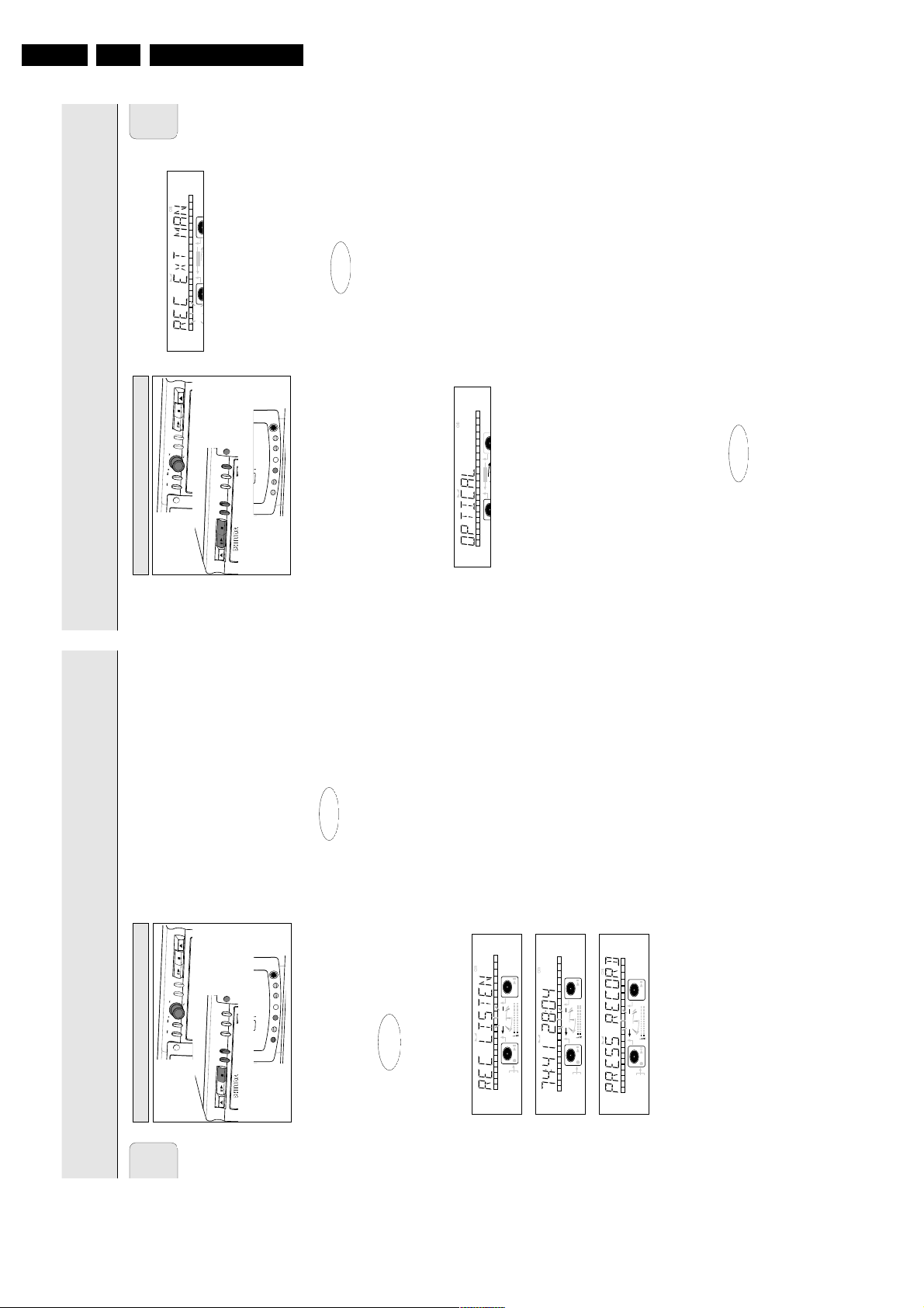
During Listen mode recording you listen to the recording
while you are making it.
Preparing for Listen mode recording
1 Make sure that the recording disc is absolutely free of
scratches and dust particles.
2 For recording, press REC TYPE twice:
➜ The display first shows the selection.
The fRECORDg label starts blinking. After 3 seconds
the display shows the remaining CDR(W) recording time
on the left and total time of source on the right. (every 2
seconds PRESS RECORD is displayed) The left
selection indicator is lit.
•If DOES NOT FIT appears on the display, there is not
enough recording space left on the CDR(W) disc.
You can press RECORD: only complete tracks that still fit on
the CDR(W) will recorded.orYou can press PROG to select one or more tracks for
recording (see programming):
- rotate the EASY JOG/ENTER key to the required track
number, then press the key (or ENTER on the remote
control)
or
- directly select the track number via the 10-keypad on the
remote control then press the ENTER key to confirm your
selection and go to the next step.
3 Play the source first to set the optimal recording level on
the CD recorder.
4 Rotate the EASY JOG/ENTER key until, on the Record/Play
Level bar, all the blue segments are alight, but the red
segments do not light continuously during the loudest
passages.
➜ Display shows _XX DB (Decibel, e.g. -3DB).
5 Stop the source.
Start Listen mode recording
1 To start recording, press RECORD.
➜ WAIT lights up. fRECORDg lights continuously and
the selected track or program is copied at normal speed.
The track number and the recording time left will appear.
•To check the track time, press DISPLAY. This can be done
during recording.
•Recording will stop automatically.
Note: Copy prohibited tracks will be copied analog.
ANALOG
REC
is displayed.
2 To stop recording, press STOP.
➜ UPDATE lights up, fRECORDg goes out and
recording stops. (Minimal track length must be 4 seconds
otherwise silence will be added to the track.)
•If STOP was pressed within 3 seconds after RECORD, no
recording will take place.
After recording, the display shows UPDATE for several
seconds. The Total time indications can differ slightly.
However, no music information is lost.
Note: In this Recording mode, the Pause function is not
operative.
Important:
If you want to play the recorded CDR disc on any
regular CD player, it must first be finalized. See
finalizing discs.
Finalized CDRW discs play only on CDRW compatible
CD players.
A
N
A
L
O
G
R
W
Listen mode recording from internal CD player
RECORDING
Directions for use
ALL
TIME STEPTRACK
REMTOTAL
TRACK
TIME
REC
REM
PROG
RECORD
SYNC MANUAL
SHUFFLE
REPEAT
CD
RW
CHANGER
CD
RW
I
I
DIGITAL
OPTICAL
TRACK
SCAN
ANALOG
S
E
N
O
H
O
C
E
R
D
C
O
I
D
U
A
9
7
7
R
D
C
P
DJ MODE
R
REPEAT
E
D
R
SCROLL
DISPLAY
SHUFFLE
PROG
L/
E
E
T
C
E
L
N
E
A
D
C
/
RE
NU
E
TO
M
S
R
R
E
D
T
C
N
E
G
O
J
Y
S
A
E
D
C
E
C
T
R
X
U
E
O
S
EF
S
A
R
E
E
Z
I
L
A
N
I
D
R
O
C
E
R
E
C
P
E
Y
R
T
P
P
O
T
TO
S
S
E
E
S
US
U
A
A
P
P
/
/
Y
Y
A
A
L
L
P
P
E
E
S
S
O
O
L
L
C
C
/
/
N
N
E
E
P
P
O
O
TIME STEPTRACK
REMTOTAL
TRACK
TIME
REC
REM
PROG
RECORD
SYNC MANUAL
ALL
TRACK
SHUFFLE
REPEAT
SCAN
CD
RW
CHANGER
CD
RW
I
I
DIGITAL
ANALOG
OPTICAL
TIME STEPTRACK
REMTOTAL
TRACK
TIME
REC
REM
PROG
RECORD
SYNC MANUAL
ALL
TRACK
SHUFFLE
REPEAT
SCAN
CD
RW
CHANGER
CD
RW
I
I
DIGITAL
ANALOG
OPTICAL
Page 13
Directions for use
English
21
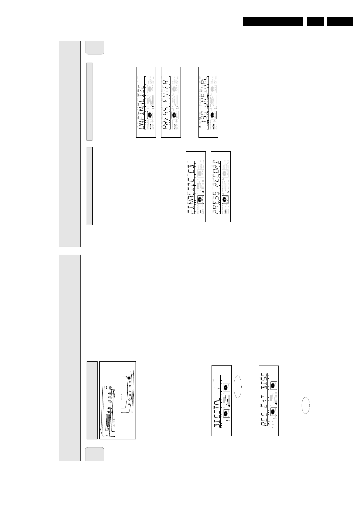
During finalizing the Table of Contents (TOC) is written to the
disc.
Finalizing is a simple procedure, necessary to:
- be able to play recordings on a CD PLAYER,
- avoid further unwanted recordings on a disc,
- avoid erasure of tracks on a CDRW,
- write CD text on a CDR(W).
Auto finalizing
Auto finalizing is possible when using the MAKE CD recording
function.
Manual finalizing
1 Make sure the disc (in the CD recorder deck) is absolutely
free of scratches and dust particles.
2 With the recorder stopped press FINALIZE.
➜ The display shows FINALIZE CD and PRESS
RECORD.
3 Press RECORD.
➜ XX XX FINAL and the approximate finalization time
appears on the display.
The display counts down through the finalization.
On completion, the total number of tracks and the total
time recorded appears on the display.
For CDR(W),
r
changes to
d
on display.
Finalizing will take at least 2 - 4 minutes.
Note:
- During finalization, the CD recorder accepts no operating
commands.
- When a CDR is finalized no more recordings can be added.
For CDRW discs only.
If you want to make more recordings (or erasures of tracks) on a
finalized disc you must unfinalize it first. The Table of Contents
(TOC) will be removed. (This is not possible for CDR discs.)
To unfinalize:
1 With the CD recorder stopped, press REC TYPE or ERASE.
➜ UNFINALIZE and PRESS ENTER will appear on
the display.
2 Press JOG (ENTER).
➜ The disc will now be unfinalized and can be recorded on
again and the Recording or Erasure mode is entered.
3 You can now start recording or erasing. If no further
recording or erasure is required press STOP 9.
Note:
- Unfinalizing will take approximately 1 minute 30 seconds.
- When unfinalizing a CDRW disc with text on it available,
this text will be transferred to the CD recorder memory. It
may occur that the text memory is full. The message
MEMORY FULL
/
FINALIZE CD
will be displayed.
To empty the recorders text memory you have to erase text
from it. This can be done in two ways:
1) Finalize one or more unfinalized discs for wich CD text is
available.
2) Delete text of unfinalized discs with the ‘memory view’
option in the Menu mode.
Unfinalizing CDRW discsFinalizing CDR & CDRW discs
RECORDING
A
N
A
L
O
G
R
W
GB 13CDR779 3.
RECORDING
recording starts at the beginning of the next track or after
•If, however, you start the source during a track, CD-SYNC
Autostart recording from external CD player
CD-SYNC
English
2.7 seconds of silence in analog recordings.
•To check the remaining recording time on the CDR(W), press
E
C
T
R
X
U
E
O
S
SEF
A
R
E
E
ALIZ
IN
D
R
O
C
E
R
E
C
P
E
Y
R
T
P
OP
T
S
STO
E
S
U
AUSE
A
Y / P
Y / P
PLA
PLA
E
E
S
S
O
O
L
L
/ C
/ C
N
N
E
E
P
P
O
O
DISPLAY. (This can also be done during recording.)
R
CD
REC EXT
and d go out.
SYNC
Finalized CDRW discs play only on CDRW compatible
CD players.
ALL
TRACK
SHUFFLE
REPEAT
SCAN
CD
RW
CHANGER
CD
RW
I
I
DIGITAL
ANALOG
OPTICAL
For recording from CD changers always use
3 With the CD recorder stopped, press REC TYPE four times:
.
DISC
start to flash and the display shows REC
SYNC
if you wish to record a complete disc or program.
➜ d and
ALL
TRACK
PROG
SHUFFLE
REPEAT
SCAN
CD
RW
TIME STEPTRACK
REMTOTAL
RECORD
CHANGER
CD
TRACK
RW
TIME
REC
I
I
REM
DIGITAL
ANALOG
OPTICAL
SYNC MANUAL
the total remaining time and START SOURCE.
EXT DISCand WAIT followed by the track number,
•If input label (DIGITAL I) flashes, the digital connection is
incorrect.
Start autostart recording
1 To start recording, press PLAY on the selected source.
lights continuously. The track number and track
SYNC
and
time appear on the display.
➜ The CD recorder automatically starts to record and d
20
resume, press RECORD on the CD recorder.
PLAY, no recording will take place.
recording level.
•The EASY JOG/ENTER key can be used to adjust the
S
E
N
O
H
P
E
D
O
M
J
D
T
A
E
P
E
R
ER
D
R
O
L
L
O
REC
R
C
D
S
C
IO
Y
D
A
L
P
AU
S
I
D
79
7
R
E
D
L
C
F
F
U
H
S
G
O
R
P
•The recorder stops automatically.
2 To stop recording manually, press STOP on the CD recorder.
The CD-SYNC feature enables you to make fast and easy
➜ UPDATE lights up and
recordings of a CD. Track increments are automatically
detected from the source material. Track increments cannot
•If STOP 9 was pressed within 3 seconds after pressing
be added manually. In analog source material a silence of 2.7
seconds or more is automatically detected as a track
•To interrupt recording, press PAUSE on the CD recorder.
increment.
➜ d starts to flash. (Autostart recording is disabled.) To
Preparing for autostart recording
1 Make sure the disc is absolutely free of scratches and dust
After recording the display will show UPDATE for several
seconds.
particles.
2 Press EXT(ernal) SOURCE repeatedly until (depending on the
Note: Auto track is always active.
digital connection used):
➜ DIGITAL I, OPTICAL I or ANALOG lights up and
Important:
If you want to play the recorded CDR disc on any
regular CD player, it must first be finalized. See
TIME STEPTRACK
REMTOTAL
TRACK
TIME
REC
REM
DIGITAL 1, OPTICAL or ANALOG appears on the
display.
finalizing discs.
PROG
RECORD
SYNC MANUAL
Page 14
GB 14 CDR7793.
English
23
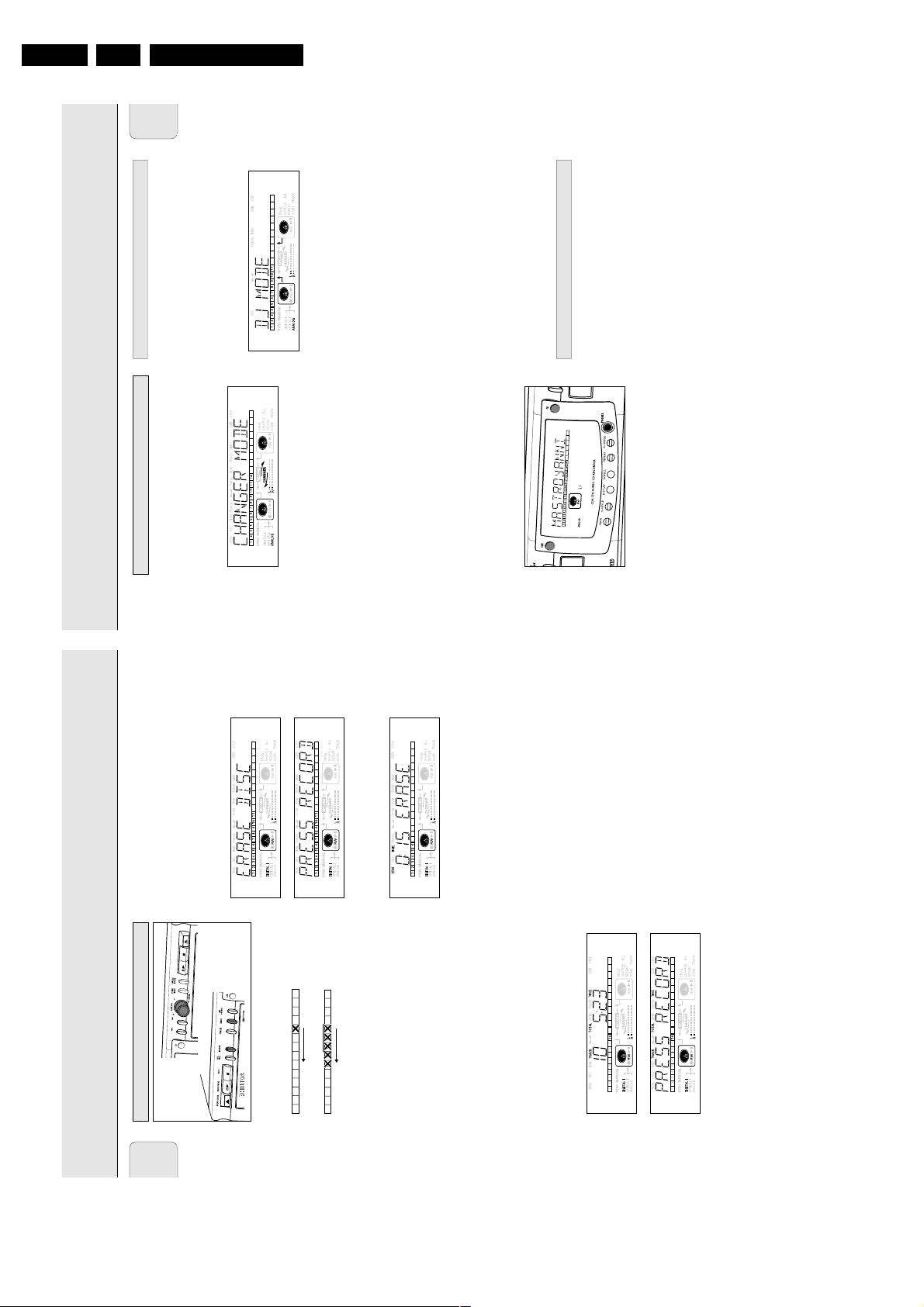
Your CD recorder is able to play the two decks sequentially
(CHANGER mode). This is the default setting.
1 Select Changer mode using the DJ MODE key.
➜ CHANGER MODE appears on the display and
iCHANGERh lights up.
2 On the deck you want to play, press PLAY/PAUSE 2;to
start CD play.
➜ 2 lights up, the track number and track time of the track
in play appear on the display.
➜ After playing the first disc the second disc will
automatically be played.
•Press DISPLAY once, twice or three times to see:
➜ remaining track time, total remaining time, permanent
text information (see Menu mode).
•To interrupt play temporarily, press PLAY/PAUSE 2;again.
➜ ; lights on the display.
•To continue play, press PLAY/PAUSE 2;again.
3 To stop play, press STOP 9.
➜ The number of tracks and the total playing time appear
on the display.
•If you want to see the information about the other deck,
press the CDR key or the CD key in the display frame.
With this double deck it is possible to play the CD recorder
deck and/or the CD player deck individually (at the same
time). In this case the extra CD output must also be connected
to an amplifier.
1 Select DJ mode using the DJ MODE key.
➜ DJ MODE appears on the display and j k lights
up.
2 On the deck you want to play, press PLAY/PAUSE 2;to
start CD play.
➜ 2 lights up and the track number and track time of the
track in play appear on the display.
•You can also play the two decks at the same time. By
pressing the CDR key or the CD key you can choose the
deck you want to listen to.
•Press DISPLAY once, twice or three times to see:
➜ remaining track time, total remaining time, permanent
text information (see Menu mode).
•To interrupt play temporarily, press PLAY/PAUSE 2;again.
➜ ; lights on the display.
•To continue play, press PLAY/PAUSE 2;again.
3 To stop play, press STOP 9.
➜ The number of tracks and the total playing time appear
on the display. If you want to see this information about
the other deck, press CDR or CD.
1 In stop mode press SCAN on the remote control.
2 The first 10 seconds of each track on the CD (or program if
set) are played.
3 Press SCAN again to return to normal CD play mode.
Intro Scan
Playing CDs on Deck 1 and/or Deck 2 (DJ mode)Play a 2-disc changer (Changer mode)
PLAYING
English
22
For unfinalized CDRW discs only.
You can erase:
- Tracks can only be erased from the end.
- With the EASY JOG you can erase more tracks.
Note: It is not possible to erase tracks within the
sequence.
- It is also possible to erase the entire disc at once.
To erase one or more tracks from the end:
1 Press ERASE once.
➜ The display shows the number of tracks and their total
playing time. ERASE TRACK and PRESS RECORD
lights up.
•If the disc is finalized,
CD
appears on the display after
inserting a CDRW in the recorder. The recorder will ask you
to confirm unfinalizing first. Confirm by pressing the EASY
JOG/ENTER key or ENTER on the remote control.
2 Select the track(s) you wish to erase by turning the EASY
JOG/ENTER key to the left.
➜ The selected track numbers start blinking on the track
bar.
➜ The display shows the remaining time after erasing the
selected track(s), the shown track will also be included
in the erasure of tracks.
3 Press RECORD.
➜ The display shows the total countdown time and
ERASE.
➜ After the selected track(s) have erased, the display
shows the remaining tracks and their total playing time.
To erase the entire disc:
1 In stop mode press ERASE twice.
➜ ERASE DISC and PRESS RECORD light up.
• If the disc is finalized,
CD
appears on the display after
inserting a CDRW in the recorder. The recorder will ask you
to confirm unfinalizing first. Confirm by pressing the EASY
JOG/ENTER key or ENTER on the remote control.
2 Press RECORD.
➜ The display shows the total countdown time and
ERASE The complete disc will be erased.
Erasure of a complete disc may take up to 15 seconds.
Erasing CDRW discs
RECORDING
Directions for use
910
678
5
4
3
2
1
910
678
5
4
3
2
1
Page 15
Directions for use
English
25
Only in Changer mode.
1 Select Changer mode, if nessesary, using the DJ MODE key.
2 Press SHUFFLE before or during CD play to start shuffle
play.
➜ The tracks on the CD (or program if set) play in random
order.
3 Press SHUFFLE again to disable the Shuffle mode.
➜ CD recorder goes to Stop mode.
Note: Shuffle is also cleared if you open the disc tray.
1 Press REPEAT one or more times during CD play.
➜ When
REPEAT TRACK
lights up, the current track plays
repeatedly. When
REPEAT ALL
lights up, the disc or
program plays repeatedly.
2 To return to normal play, press REPEAT one or more times
until:
➜ the
REPEAT
label disappears from the display.
Note:
- You can use shuffle in combination with
REPEAT ALL
or
programmed play of the 2-disc changer.
-
REPEAT
is also cleared if you open the disc tray.
Repeat CD, track or programShuffle (random order) play
PLAYING
GB 15CDR779 3.
PLAYING
SearchSelecting a track
English
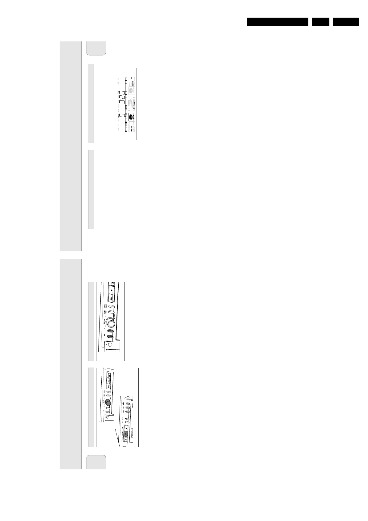
1 Hold down 5 or 6 (in play mode).
search is restricted to within the track being played at
➜ Play starts at the desired passage.
number appears on the display.
1 Turn the EASY JOG/ENTER key until the required track
Note: During Shuffle, Repeat Track or Programmed play,
➜ Play skips to the beginning of the selected track.
the time.
subsequent tracks, including tracks on the disc in the
or CDR as applicable.
➜ Play skips to the beginning of the selected track.
or
➜ Play skips to the beginning of the present, previous or
Select CDR or CD on the remote control and key in the
required track number using the numerical keys on the
remote control. For 2-digit track numbers, press the keys in
rapid succession. For tracks on the other disc, first press CD
or
other deck. (Changer mode only.)
Press ¡ or ™ on the remote control one or more times.
Selecting a track when CD play is stopped
1 Turn the EASY JOG/ENTER key until the required track
number appears on the display.
confirm or press PLAY/PAUSE 2;to start playing.
required track number using the numerical keys. For 2-digit
track numbers, press the keys in rapid succession. Play
2 Press EASY JOG/ENTER or ENTER on the remote control to
starts.
or
1 Select CDR or CD on the remote control and key in the
JOG/ENTER or ENTER on the remote control.
or
1 Briefly press ¡ or ™ one or more times.
2 Start playback by pressing PLAY/PAUSE 2;, EASY
24
times normal speed with sound at low volume, then
goes to 50 times normal speed with sound muted.
➜ The player first searches backwards or forwards at 10
2 Release the button at the desired passage.
Selecting a track during play
Page 16
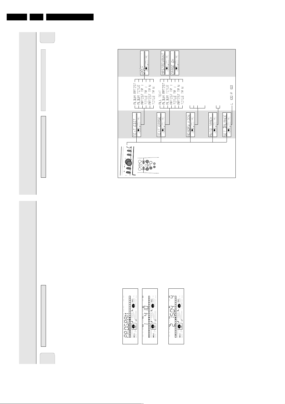
GB 16 CDR7793.
•In Menu mode you will have access to a number of features
which are not available via the regular keys (on the deck’s
front and the remote control).
•The TEXT submenus (A-B) allow you to give names to discs
and tracks. The disc and track names will be displayed
during playback.
•In the RECORDING submenus (D-E) you can set Auto Track
and Balance.
•All settings (except Balance) made in Menu mode will be
stored in the deck’s memory and can be called up and
changed at any time.
Menu active in Recording or Stop mode.
1 When using the remote control select first CDR.
2 Press STORE/MENU on the deck or the remote control to
enter Menu mode.
➜ TEXT EDIT appears on the display.
3 Rotate EASY JOG/ENTER to select the required submenus.
4 Press EASY JOG/ENTER to confirm selections.
5 Rotate EASY JOG/ENTER to select options in the submenus.
6 Press EASY JOG/ENTER to confirm selections.
7 Press STORE/MENU to store settings and return to the
submenu.
8 Press STOP 9 to store settings and exit Menu mode.
Note: Text can only be edited for unfinalized discs. (Finalized
CDRW discs must be unfinalized first.)
General operation of MenuRemarks about Menu mode
MENU MODE
English
27
E
A
S
Y
J
O
G
S
T
O
R
E
/
M
E
N
U
C
A
N
C
E
L
/
D
E
L
E
T
E
E
N
T
E
R
MENU/
STORE
PROG.
ENTER CANCEL
CDR
2
9
;
KJ
56
CD
"TITLE CD 1"
"TITLE CD 2"
"TITLE CD 3"
"TITLE CD n"ONOFF
MAIN MENU LEVEL 2LEVEL 1
A
B
C
D
E
REM
TRACK
REC
TIME
DIGITAL
OPTICAL
ANALOG
PROG
SHUFFLE
REPEAT
SCAN
I
I
CD
RW
CHANGER
SYNCMANUAL
RECORD
REMTOTAL
ALL
TRACK
TIME STEPTRACK
CD
RW
123456789
1011 12 13 14 15 16 17
REM
TRACK
REC
TIME
DIGITAL
OPTICAL
ANALOG
PROG
SHUFFLE
REPEAT
SCAN
I
I
CD
RW
CHANGER
SYNCMANUAL
RECORD
REMTOTAL
ALL
TRACK
TIME STEPTRACK
CD
RW
123456789
1011 12 13 14 15 16 17
REM
TRACK
REC
TIME
DIGITAL
OPTICAL
ANALOG
PROG
SHUFFLE
REPEAT
SCAN
I
I
CD
RW
CHANGER
SYNCMANUAL
RECORD
REMTOTAL
ALL
TRACK
TIME STEPTRACK
CD
RW
123456789
1011 12 13 14 15 16 17
REM
TRACK
REC
TIME
DIGITAL
OPTICAL
ANALOG
PROG
SHUFFLE
REPEAT
SCAN
I
I
CD
RW
CHANGER
SYNCMANUAL
RECORD
REMTOTAL
ALL
TRACK
TIME STEPTRACK
CD
RW
123456789
1011 12 13 14 15 16 17
REM
TRACK
REC
TIME
DIGITAL
OPTICAL
ANALOG
PROG
SHUFFLE
REPEAT
SCAN
I
I
CD
RW
CHANGER
SYNCMANUAL
RECORD
REMTOTAL
ALL
TRACK
TIME STEPTRACK
CD
RW
123456789
1011 12 13 14 15 16 17
REM
TRACK
REC
TIME
DIGITAL
OPTICAL
ANALOG
PROG
SHUFFLE
REPEAT
SCAN
I
I
CD
RW
CHANGER
SYNCMANUAL
RECORD
REMTOTAL
ALL
TRACK
TIME STEPTRACK
CD
RW
123456789
1011 12 13 14 15 16 17
REM
TRACK
REC
TIME
DIGITAL
OPTICAL
ANALOG
PROG
SHUFFLE
REPEAT
SCAN
I
I
CD
RW
CHANGER
SYNCMANUAL
RECORD
REMTOTAL
ALL
TRACK
TIME STEPTRACK
CD
RW
123456789
1011 12 13 14 15 16 17
REM
TRACK
REC
TIME
DIGITAL
OPTICAL
ANALOG
PROG
SHUFFLE
REPEAT
SCAN
I
I
CD
RW
CHANGER
SYNCMANUAL
RECORD
REMTOTAL
ALL
TRACK
TIME STEPTRACK
CD
RW
123456789
1011 12 13 14 15 16 17
•You can program up to 99 tracks to play in any desired
sequence.
•Tracks can be programmed more than once, but each time
counts as a track. (
STEP
)
•A program for playback can be made from both the disc in
the recorder deck and the disc in the player deck. A program
for recording can only be made from the disc in the player
deck.
Programming for playback
1 Select Changer mode or DJ mode using the DJ MODE key.
➜ CHANGER MODE or DJ MODE appears on the display.
2 Press CDR or CD to select the required deck.
➜ Selected key lights up.
3 Press PROG(ram) to enter Program mode.
➜
PROG
flashes and PROGRAM followed by track
information appears on the display.
4 Select the required track numbers by turning the EASY
JOG/ENTER key left or right and store by pressing ENTER.
or:
Key in a track number with the number keys on the remote
control and press ENTER to confirm. For 2-digit numbers,
press the keys in rapid succession.
➜ The track will be stored in the program.
➜ The track number, total program time and the number of
programmed tracks (
STEP
) are displayed.
5 Repeat step 4 for all tracks to be programmed.
6 Press STOP or PROG(ram) to end programming.
➜
PROG
lights continuously.
7 Press PLAY/PAUSE 2; to start programmed play.
Note:
- To review the program, press PROG(ram), followed by
5
or
6
with the CD player or CD recorder in stop mode.
- To add more tracks to the program, repeat steps 2 to 6.
- If you try to store more than 99 tracks,
PROG FULL
appears on the display.
Programming for recording
1 Press REC TYPE to select the required recording mode (see
‘Recording’).
2 Compile your programme as described in “programming for
playback”. (steps 3 to 5)
•Only tracks from the disc in the CD player can be stored.
3 Press RECORD to start recording.
Clearing a program
1 Press STOP 9 if necessary to stop programmed play.
2 Press STOP 9 again to clear the program.
➜
PROG
disappears from the display.
•The program is also cleared if you open the disc tray.
Erasing a track from a program
1 In Stop mode press PROG(ram) to enter Program mode.
2 Use 5 or 6 to select the track that has to be deleted.
➜ The track number and program step will be shown on
the display.
3 Press CANCEL/DELETE to erase the track from the program.
➜ The remaining program steps and the remaining playing
time of the program will be displayed.
4 Repeat step 2 and 3 for all tracks to be erased.
5 Press STOP 9 or PROG(ram) to end erasing.
➜
PROG
lights continuosly.
Remarks about programming
PROGRAMMING
English
26
Directions for use
Page 17
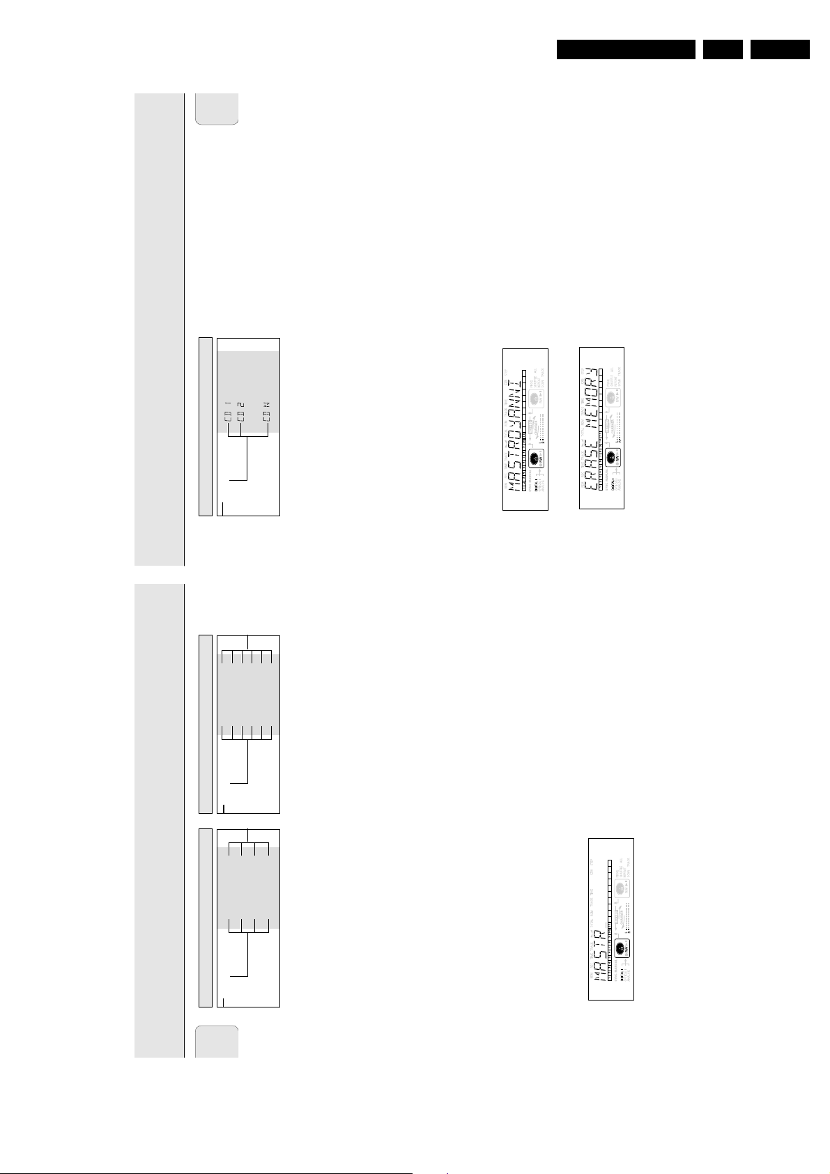
Directions for use
CD Text is stored in the recorders memory. When a CDR(W)
will be finalized the CD Text will be written on the disc and
removed from the recorders memory. With the MEMORY
VIEW function one can view/delete the CD Text in the
recorders memory per unfinalized disc. The amount of memory
used is displayed each time the tray opens with an
unfinalized CDR(W) inserted.
(e.g. MEMORY 9%)
1 Press STORE/MENU.
➜ TEXT EDIT appears on the display.
2 Rotate the EASY JOG/ENTER key to select the MEMORY
VIEW submenu.
➜ MEMORY VIEW appears on the display.
3 Press EASY JOG/ENTER to confirm.
➜ The first album title in the recorder memory appears on
the display.
4 Select the album title you wish to erase by rotating the
EASY JOG/ENTER key.
5 Press EASY JOG/ENTER to confirm.
➜ ERASE MEMORY appears on the display.
6 Press the EASY JOG/ENTER key to confirm the erasure of
the text for that particular disc.
➜ UPDATE appears on the display.
7 Press STORE/MENU to return to the submenu or STOP 9 to
exit.
Note:
- If there are no discs in the memory, the message
MEMORY
EMPTY
appears on the display.
- When the text memory of your CD recorder is full, the
message
MEMORY FULL
will appear, followed by
FINALIZE CD
. If you want to add a CD to the list of
discs for which text is stored, you have to erase a disc from
this list or finalize another disc. (“for which text is stored”)
-
MEMORY FULL
/
FINALIZE CD
may also appear when
unfinalizing a CDRW disc for which text was stored (see
‘Unfinalizing CDRW discs’). The same action(s) should be
taken in order to obtain memory space.
MEMORY VIEW
C. Reviewing CD Text in memory/memory view
MENU MODE/CD TEXT
English
29
GB 17CDR779 3.
ALL TEXT
ALBUM ARTIST
ALBUM TITLE
ARTIST TR N
TITLE TR N
NO TEXT
(When there is no text available the message NO TEXT
TEXT ERASE
MENU MODE/CD TEXT
B. Erasing text/text erase
ALBUM ARTIST
TEXT EDIT
A. Text input/text edit
ALBUM TITLE
ARTIST TR N
1 Press STORE/MENU.
TITLE TR N
CD Text can be added to a recording or changed.This can be
➜ TEXT EDIT appears on the display.
done in Stop mode or during recording.
2 Rotate the EASY JOG/ENTER key to select the TEXT ERASE
Text will be stored in the recorder memory and can be edited
submenu.
➜ TEXT ERASE appears on the display.
until the CDR is finalized. Text on a (unfinalized) CDRW can be
edited at any time.
appears on the display.)
➜ If text is available ALL TEXT appears on the display.
3 Press EASY JOG/ENTER to confirm.
➜ TEXT EDIT appears on the display.
1 Press STORE/MENU.
2 Press EASY JOG/ENTER to confirm.
the submenu: ALL TEXT, ALBUM ARTIST, ALBUM
4 Rotate EASY JOG/ENTER to select the required option in
➜ ALBUM ARTIST appears on the display.
3 Rotate EASY JOG/ENTER to select the required option in
ERASE OK appears on the display.
TITLE, ARTIST TR 1, TITLE TR 1, etc.
➜ The display will ask you to reconfirm your selection.
5 Press EASY JOG/ENTER to confirm.
the submenu: ALBUM ARTIST, ALBUM TITLE,
ARTIST TR 1, TITLE TR 1, etc.
➜ The first character space appears on the display.
4 Press EASY JOG/ENTER to confirm.
➜ UPDATE appears on the display.
6 Press EASY JOG/ENTER to reconfirm.
or by pressing the corresponding numeric/alphabet key on
5 Select the characters by rotating the EASY JOG/ENTER key
7 Press STORE/MENU to return to the submenu or STOP 9 to
the remote control.
exit.
6 Press EASY JOG/ENTER to store each character and move
to the next cursor position.
• With the 5 6 keys you can move to a required cursor
position.
• With the CANCEL key you can delete a character.
return to the submenu resume at 3 or STOP 9 to exit.
7 Press STORE/MENU to store a name you have entered and
Note:
- A maximum of 60 characters can be stored per item.
- By pressing the EASY JOG/ENTER key or ENTER on the
remote control without selecting a character first, you can
insert a space between characters.
- When an artist’s name has been stored for a certain track,
the name will automatically be copied for the next track.
The name can be confirmed by pressing STORE/MENU or a
new name can be entered as described above.
28
English
Page 18
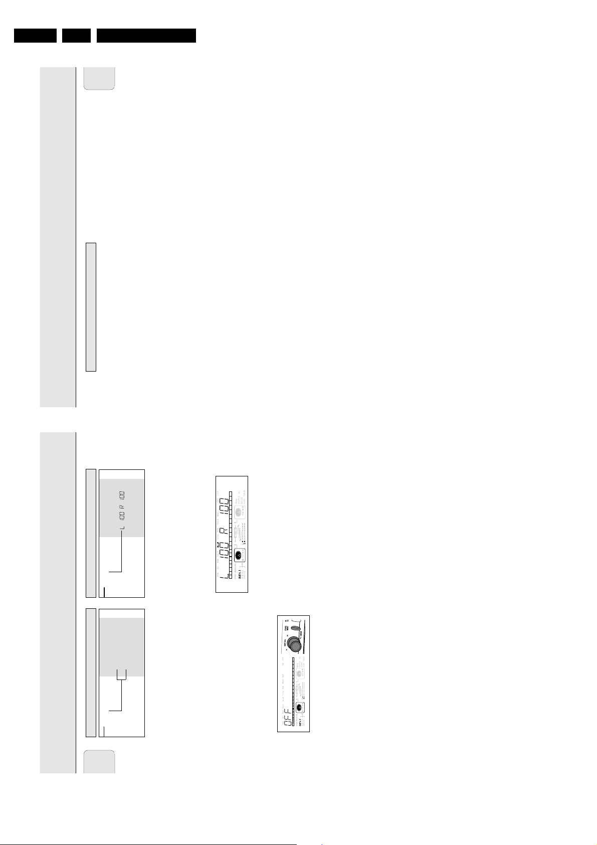
GB 18 CDR7793.
If your CD recorder is defective, it is wise to check this list
first. You may have forgotten a simple step.
Warning!
Under no circumstances should you attempt to repair
the CD recorder yourself as this will invalidate the
guarantee.
SYMPTOM • possible solution:
No power • ensure that the ON/OFF button is on (red led
on): the CD Recorder is in standby mode,
press any key to activate it
• ensure that the mains cable is plugged in
correctly
• switch the recorder OFF and then
immediately back ON
Auto track does not work
• check if auto track on is selected in the menu
• check if there are 2.7 seconds silence in
between the tracks (analog recording only)
• check if the source is a consumer source with
the digital output according to the IEC audio
standard
• source is DVD player (no track information)
No sound • check the audio connections
• if using an amplifier, try using a different
source
Amplifier sound is distorted
• check that the CD recorder analog output is
not connected to the amplifier Phono input
Play will not start
• ensure that the label of the CD is facing up
• clean the disc
• check that the disc is not defective by trying
another disc
Remote control does not work
• point the remote control towards the CD
recorder
• check the batteries and replace if necessary
• select the correct source first
Will not record
• clean the disc
• check if CDR(W) is an unfinalized disc
• check that the disc is recordable and replace
if necessary
• the disc is not an AUDIO disc (WRONG
DISC)
• wrong input source chosen. Input label
flashing (CHECK INPUT)
• text memory full (MEMORY FULL/
FINALIZE CD). When a CDRW has to be
unfinalized for recording. Erase text for other
disc(s) or finalize other disc(s) to obtain
memory space
• total remaining time not sufficient, try
programming tracks (see programming)
Recording is distorted
• make sure the recording level is correct
20 second pause between recordings
• see Autostart recording from external CD
player (CD-SYNC)
Player does not react
• switch the ON/OFF button on the front of the
player off and back on
DISC RECOVER on display
• a power failure has occurred during
recording, the CD recorder is attempting to
repair the disc
• if DISC ERROR then appears on the
display, the disc cannot be recorded further,
and cannot be finalized. But it can still be
played on the CD recorder or another CD
recorder
• on a CDRW disc, the track being recorded is
lost, but further recording and finalization can
still be done
TROUBLESHOOTING
FIXING PROBLEMS
English
31
1 Press STORE/MENU.
➜ TEXT EDIT appears on the display.
2 Rotate the EASY JOG/ENTER key to select the AUTO TRACK
submenu.
➜ AUTO TRACK appears on the display.
3 Press EASY JOG/ENTER to confirm.
➜ ON or OFF appears on the display.
4 Turn the EASY JOG/ENTER key to select Auto track ON or
OFF.
•When ON is selected, track numbers will be automatically
incremented during recording.
•When OFF is selected, you can number the recorded tracks
yourself.
5 Press EASY JOG/ENTER to confirm.
➜ AUTO TRACK appears on the display.
6 Press STORE/MENU to store settings and return to the
submenu or STOP 9 to exit.
1 Press STORE/MENU.
➜ TEXT EDIT appears on the display.
2 Rotate the EASY JOG/ENTER key to select the SET
BALANCE submenu.
➜ SET BALANCE appears on the display.
3 Press EASY JOG/ENTER to confirm.
➜
FE
and L 100 R 100 appear on the display.
4 Adjust recording balance by turning the EASY JOG/ENTER
key.
•Turn left: the figure left (
F
) counts down, right counts up.
•Turn right: the figure right (
E
) counts down, left counts up.
5 Press EASY JOG/ENTER to confirm.
6 Press STORE/MENU to store settings.
Note: The balance setting will not be stored permanently.
E. Balance (only active in Record/Standby mode)
D. Auto track increment/auto track
MENU MODE/RECORDING SETTINGS
English
30
Directions for use
SET BALANCE
AUTO TRACK
ON
OFF
Page 19
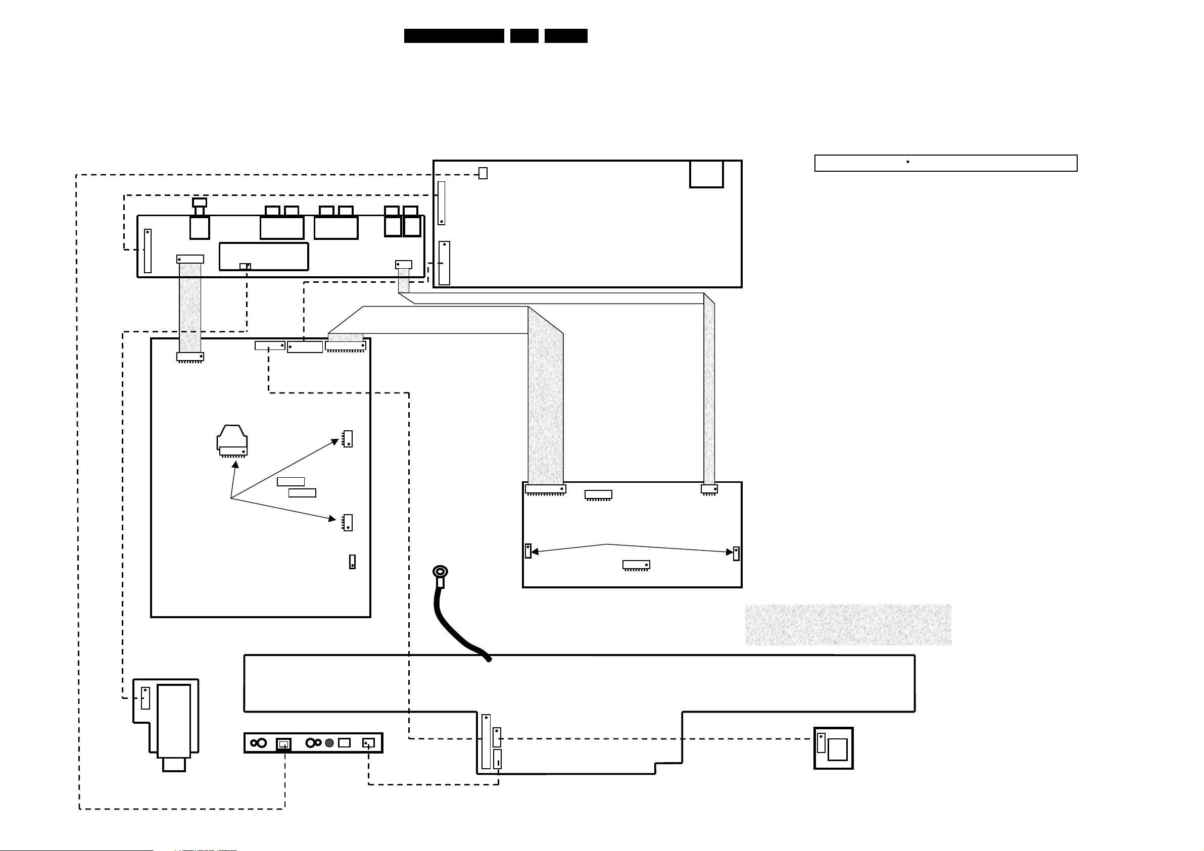
4. Mechanical instructions
Wiring diagram
WIRING DIAGRAM CDR779
Mechanical instructions
GB 19CDR779 4.
8001
3104 157 1168
8006
3104 157 1099
1
1400
1401
130
7
8010
1148
3104 157
30
1820
MAINBOARD CDR
3104 128 0648
8004
3104 157 11002
1400
1
3
HEADPHONE BOARD
3104 128 0590
3104 128 06621
1104
3
10
1
130
1000
Flex
Delivered with loader assy.
I/O BOARD
3104 128 0661
1
3104 157
1705
HP
8002
1105
1
111
1500
Cable
Connected to loader assy.
22
ON/OFF & STBY LED
3104 128 0590
1302
1200
1708
10
11
Pin 1 indicated by All Wires are 1/1.
7
207
1
1
1101
17
1
1220
1
1330
1
4
1
1300
1
2
3104 157
3104 157 1123
8003
3104 157 1149
8009
03881
205
11
8005
206
DISPLAY BOARD
3104 128 0590
1119
1
1
1122
3
1121
10
POWER SUPPLY UNIT
3122 427 21573
1000
1
1208
22
1
1002
4
Flex
Delivered with loader assy.
Cable
Connected to loader assy.
3104 157 1132
MAINBOARD CD
3104 128 0598
1006
11
Delivered with loader assy.
1
Flex
8007
7
1209
1
1001
1
4
3104 157
8008
8001
1 GROUND
2 +12V
3 GROUND
4+5V
5 GROUND
6-8V
7 Doesn't exist
CWAS 06EH/06EH 300 24S
8004
1 LEFT_HP_OUT
2 GROUND
3 RIGHT_HP_OUT
CWAS 03PH/03PH 440 26S
8005
1 GROUND
2 DSA_DATA_ CD
3 GROUND
4 DSA_ACK_CD
5 DSA_STR_CD
6 GROUND
7D5V
8 12V_CD
9 GROUND
10 IIS_WS_CD
11 IIS_BCLK_CD
12 GROUND
13 IIS_DATA_CD
14 GROUND
15 DOBM_CD
16 RESET_CD
17 LEFT_IN_CD
18 GROUND
19 RIGHT_IN_CD
20 KILL
21 SYS_CLK_8W
22 GROUND
CWAS FLEX 1mm 22 320 32S
Texture indicates text on flex
1200
1
11281
3
8002
1 VDC2
2VFTD
3 VDC1
4 GROUND
5+5V
6+5V
7GROUND
8GROUND
9GROUND
10 +12V
11 -8V
CWAS 11EH/11EH 240 24S
8007
1LEFT_CD
2GND
3RIGHT_CD
4GND
5 DOBM_CD
6 GROUND
7 KILL
CWAS FLEX 1.25mm 7 300 32S
8008
1+5V
2 IR_IN
3 GROUND
CWAS 03EH/03EH 240 24S
8009
1LED_ON
2GROUND
CWAS 02PH/02PH 120 26S
IR BOARD
3104 128 0590
8003
1 VDC2
2 VFTD
3 VDC1
4 SYS_RESET
5IIC_DATA
6GROUND
7IIC_CLK
8 DISPL_INT
9 GROUND
10 D5V
CWAS 10PH/10EH 440 26S
8006
1ON!
2 OFF!
CWAS 02EH/02EH 560 26S
8010
1 GROUND
2OPT_IN
3 DIG_OUT
4 GROUND
5DIG_IN_2
6DIG_IN_1
7 GROUND
8NC.
9 KILL_MAIN
10 DEEMP
11 MUTE
12 MICPRES_INTCOPY
13 LEVEL_A2
14 LEVEL_A1
15 LEVEL_A0
16 GROUND
17 PST3
18 +5Vd
19 IIS_DATA_ADC
20 IIS_BCLK_MIC
21 GROUND
22
IIS_WS_MIC
23 IIS_DATA_DAC
24 GROUND
25 IIS_BCLK_DAC
26 IIS_WS_DAC
27 GROUND
28 MIC_HPSEL
29 CL11_MIC
30 GROUND
CWAS FLEX 0.5mm 30 130
CL 06532151_001.eps
231100
Page 20
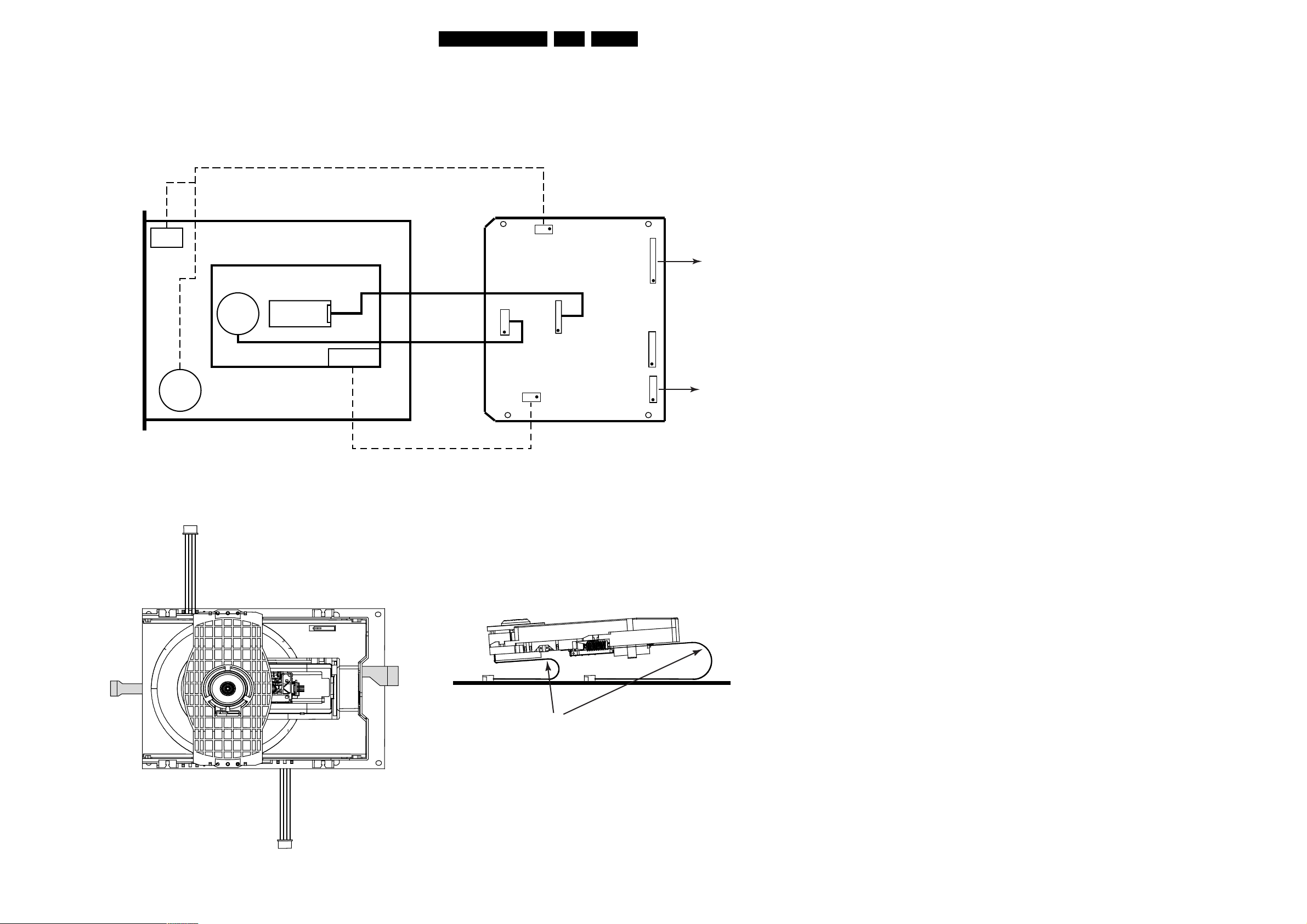
Mechanical instructions
Wiring CD
WIRING DIAGRAM CD LOADER VAL1250
GB 20CDR779 4.
Flex from
turn table motor
Tray
switch
Turn table
motor
Tray motor
Connector from tray motor
and tray switch
Connection tray motor
and tray switch
LOADER VAL1250
CDM VAM1250
OPU
LOADER VAL1250
Sledge motor
and switch
Flex from OPU
Flex from
turn table motor
Connection sledge motor
and sledge switch
Flex from OPU
CONNECTOR 1006
1 HALL +
2 W3 W+
4 V+
CONNECTOR 1002
1 HOMESW
2 SGND
3 TRAY+
4 TRAY5 HALL6 U+
1002
14
22
7 V8 U9 UCOIL
1208
1
11
1006
1
16
1000
1
MAIN BOARD CD
1001
14
16
1210
1
7
1209
1
To main board CDR
To CD out board
10 VCOIL
11 WCOIL
CONNECTOR 1000
1 VSUB
2 HFGND
3 VDD
4 RF
5 LDON
6 R2
7 R1
8 D4/D3
CONNECTOR 1001
1 HOMESW
2 SGND
3 SL-
4 SL+
CONNECTOR 1209
1 AUDIO R (RIGHT_CD)
2 GND
3 AUDIO L (LEFT_CD)
4 GND
5 DOBM5_CD (DOBM_CD)
6 GND
7 KILL
9 D2
10 D1
11 FTC
12 RW
13 FOC+
14 FOC15 RAD+
16 RAD-
CONNECTOR 1208
1 GND
2 CRIN (SYS_CLK_8W)
3 KILL
4 AUDIO R (RIGHT_IN_CD)
5 GND
6 AUDIO L (LEFT_IN_CD)
7 DSA_RST (SYS_RESET)
8 DOBM (DOBM_CD)
9 GND
10 SCLK (I2S_BCLK_CD)
11 GND
12 WCLK (I2S_WS_CD)
13 DATA (I2S_DATA_CD)
14 GND
CDM VAM1250
15 +12V
16 +5V
17 GND
18 DSA_ACK (DSA_ACK_CD)
19 DSA_STROBE (DSA_STR_CD)
20 GND
21 DSA_DATA (DSA_DATA_CD)
22 GND
Connector from sledge motor
and sledge switch
POSITION OF FLEX CONNECTIONS
MAIN BOARD CD
CL 96532086_002.eps
080999
Page 21
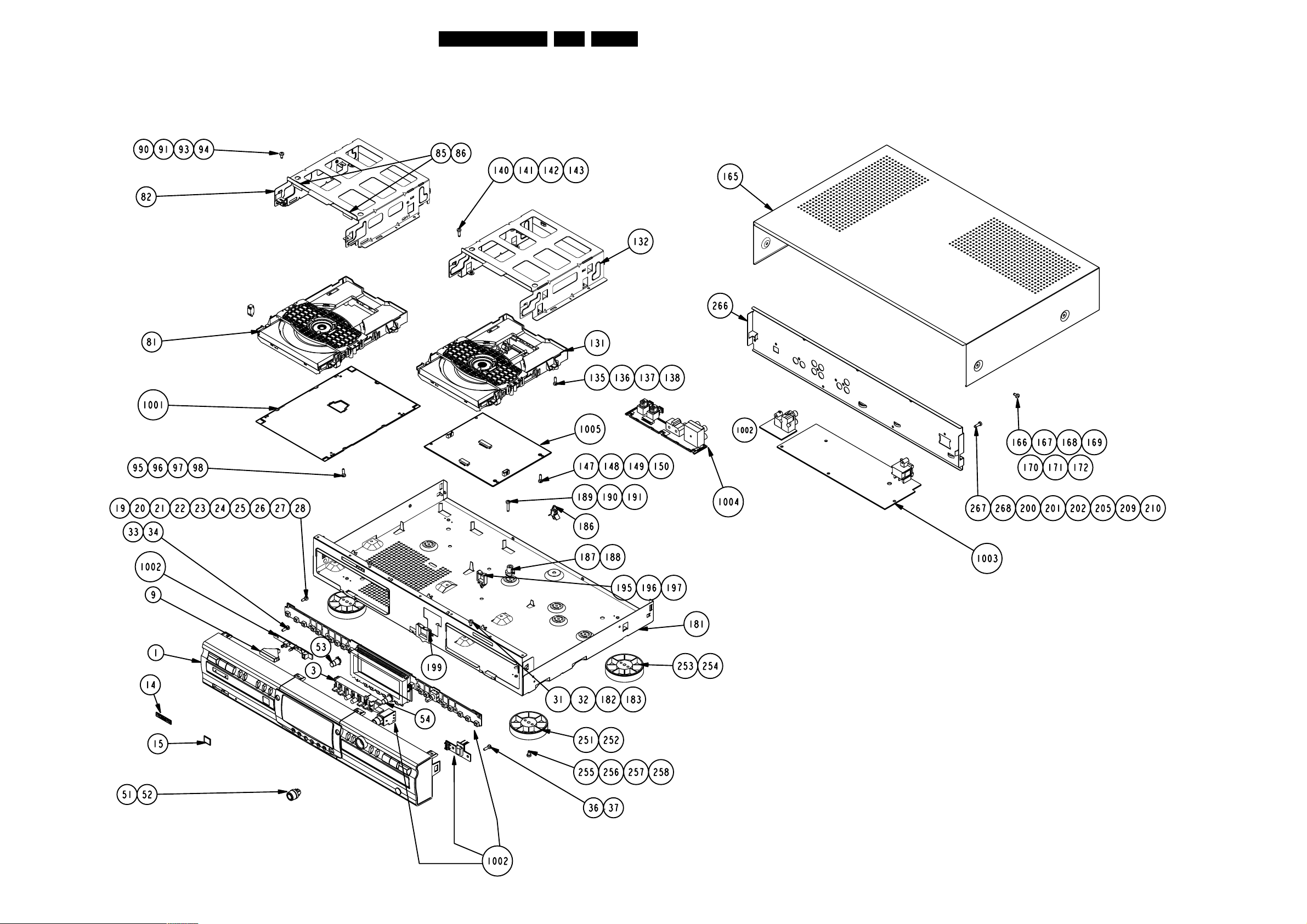
Exploded view CDR779
EXPLODED VIEW CDR779
Mechanical instructions
GB 21CDR779 4.
ON/OFF
& STBY LED
LOADER ASSY CDR
MAIN BOARD CDR
MAIN BOARD
CD
LOADER ASSY CD
CD OUT
BOARD
I/O BOARD
POWER SUPPLY UNIT
HEADPHONE
BOARD
IR
BOARD
DISPLAY
BOARD
DISPLAY ASSY
CL 06532151_015.eps
241100
Page 22
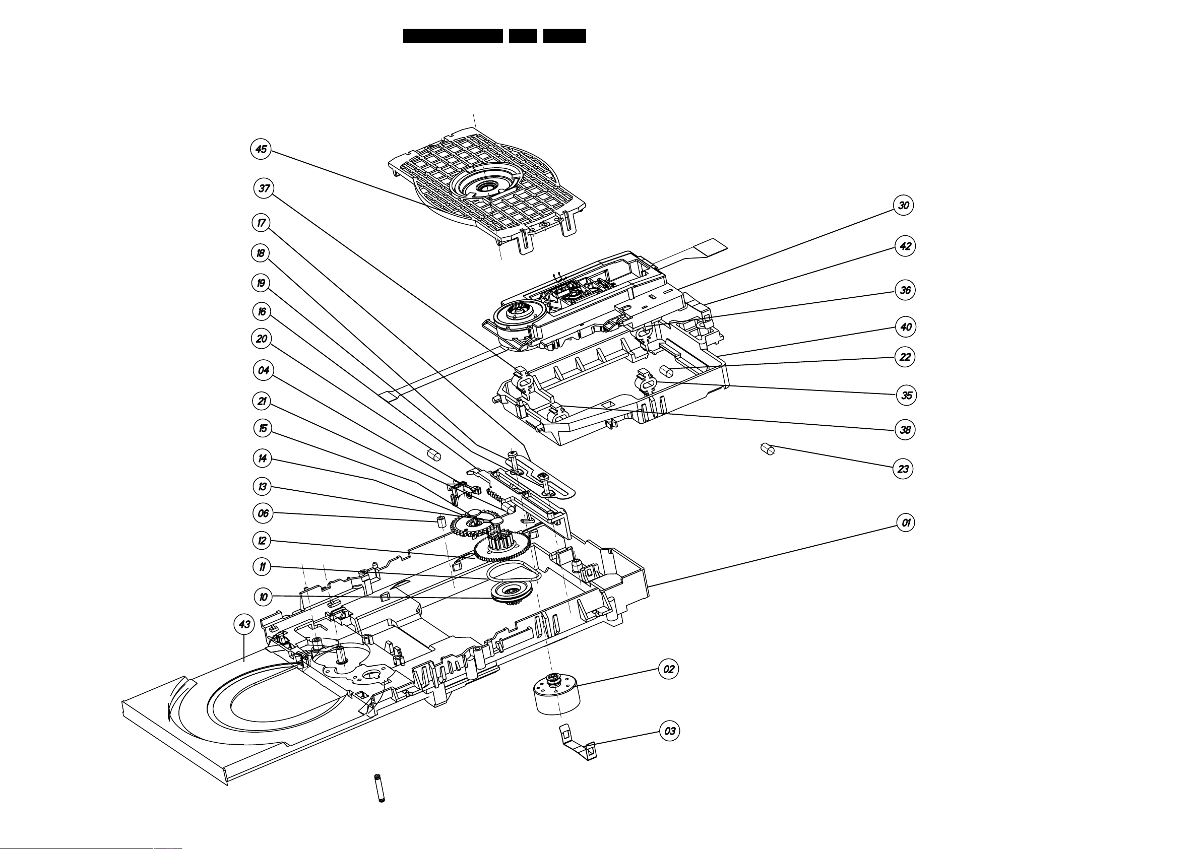
Exploded view CD
EXPLODED VIEW CD LOADER VAL1250
CLAMPER ASSY
SUSPENSION
RACK SPRING
Mechanical instructions
GB 22CDR779 4.
CDM VAM1250
SCREW
SCREW
RACK
RUBBER
SWITCH
RUBBER
PLUG
TRAY GEARWHEEL
PLUG
TULE
MOTORSPRING
SUSPENSION
SUB CHASSIS
RUBBER
SUSPENSION
SUSPENSION
RUBBER
CHASSIS ASSY VAL1250
RACK GEARWHEEL
PULLEY WHEEL
TRAY HORIZONTAL
BELT
TRAY MOTOR ASSY
MOTORSPRING
CL 96532086_004.eps
080999
Page 23
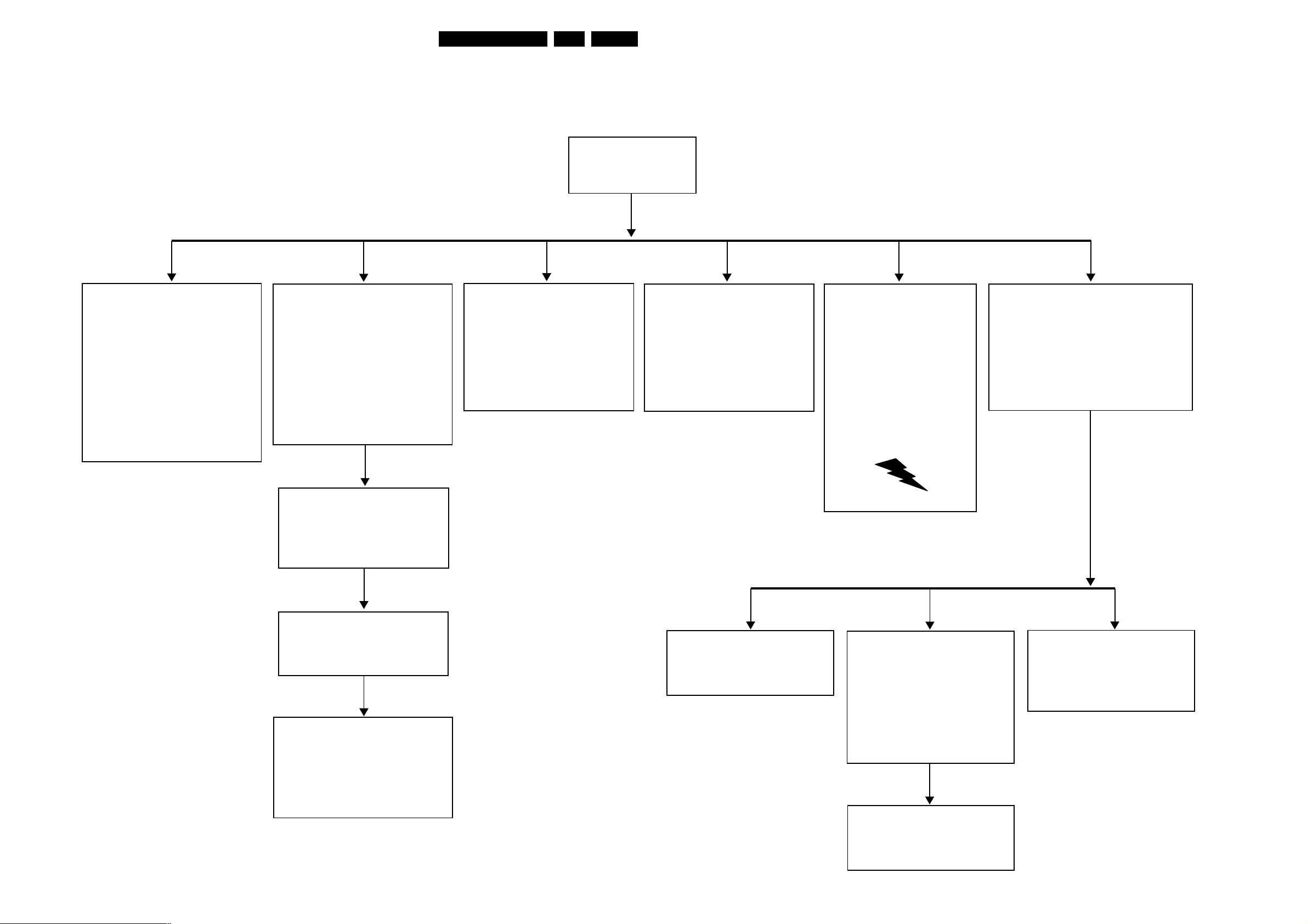
Dismantling 779
DISMANTLING INSTRUCTIONS CDR779
See exploded views for item numbers
Mechanical instructions
GB 23CDR779 4.
CDR module includes :
Loader 81
CDR main board 1001
Loader bracket 82
⇒
Put the CDR player's rear side facing you.
Undo the 3 wire connections on the CDR
⇒
main board 1001.
⇒
Undo the 2 flex connections on CDR main board.
⇒ Remove 4 screws 90,91,93,94
(loader bracket 82 → frame 181).
⇒
Lift CDR module at rear side to remove.
Attention : flexes are not part of the CDR module
and have to stay with CDR player in case
of CDR module exchange !
CD module includes :
Loader 131
CD main board 1005
Loader bracket 132
⇒
Put the CDR player's rear side facing you.
⇒ Remove 4 screws 140 → 143
(loader bracket 132 → frame 181).
⇒
Lift CD module at rear side to remove.
⇒
Undo the 2 flex connections on CD main board.
Attention : flexes are not part of the CD module
and have to stay with CDR player in case
of CD module exchange !
⇒
Remove 7 screws 166 → 172,
2 at each side and 3 at rear side.
Lift cover at rear side to remove.
⇒
CD out board 1002
⇒
Put CDR player's rear side facing you.
⇒
Undo flex connection to CD main board 1005.
⇒ Remove 2 screws 209, 210 connecting
the 2 I/O sockets to back plate 266.
⇒
Remove board.
Attention : flex is not part of the CD out board
and has to stay with CDR player in case
of CD out board exchange !
Cover 165
assembling
↑
↓
disassembling
I/O board 1004 Power supply unit 1003
⇒
Put CDR player's rear side facing you.
⇒
Undo flex connection to CDR main board 1001.
⇒
Remove 3 screws 200 → 202, connecting
the 3 I/O sockets to back plate 266.
⇒
Remove board.
Attention : flex is not part of the I/O board
and has to stay with CDR player in case
of I/O board exchange !
⇒
Put the CDR player's rear side facing you.
⇒
Undo the 2 wire connections on PSU.
⇒ Remove screw 205
(mains connector → back plate 266).
Remove 3 screws 189 → 191
⇒
(PSU board → frame 181).
⇒
Unlock snap on spacer 186.
⇒
Remove PSU.
WARNING: POSSIBILITY OF HIGH
VOLTAGE (300V) ON HEAT SINK,
EVEN AFTER REMOUNTING OF
PCB. DISCHARGE ELCAP 2121.
Front assy 1
⇒
Put the CDR player's front side facing you.
⇒
Remove 2 screws 31, 32
(ground wires
⇒
Remove 2 screws 182, 183
(front assy 1
Unlock front assy from frame by releasing 7 snaps :
⇒
start with 2 on the top and two on the sides
and end with 3 at the bottom.
⇒
After disassembly put in front of the set (service position).
→ frame 181).
→ frame 181).
CD main board 1005
⇒ Remove 4 screws 147 → 150
(CD main board → loader bracket 132).
Undo 2 flex and 2 wire connections
⇒
on CD main board.
⇒
Remove board.
CD loader assy 131
⇒ Remove 4 screws 135 → 138
(CD loader → loader bracket 132).
⇒
Remove loader.
CDM VAM1250
Remove clamper assy 45 by releasing 4 snaps
⇒
(2 on left 2 on right side) on chassis assy 1.
⇒
Open tray 43 by unlocking rack 16.
⇒
Undo wires of CDM VAM1250 from
wire retainers on sub chassis 40.
⇒ Unlock suspensions 35 → 38 from sub chassis 40.
⇒ Remove CDM VAM1250.
IR board 1002
Remove 2 screws 36 and 37
⇒
⇒
⇒
→ front assy 1).
(IR board
Undo wire connection on board.
Remove board.
Display board 1002
⇒
Remove easy jog knob 51 pulling it forward.
Remove 11 screws 19
⇒
(display board → front assy 1).
⇒
Release 2 snaps (1 on left and 1 on right side)
⇒
Undo the 3 wire connections on display board.
⇒
Remove display board.
Attention : when reassembling make sure
the wiring from display board to IR board is
positioned between FTD display and
middle key assy 3 !
→ 29
Headphone board 1002
⇒
Pull board out of front assy 1.
⇒
Slide board out of middle key assy 3.
⇒
Undo wire connection on board.
⇒
Remove board.
On/Off & Stby LED board 1002
⇒ Remove 2 screws 33 and 34
(on/off switch
⇒
Undo the 2 wire connections on board.
⇒
Remove power button 9 from on/off switch.
⇒
Remove board.
→ front assy 1).
CL 06532151_016.eps
241100
Page 24
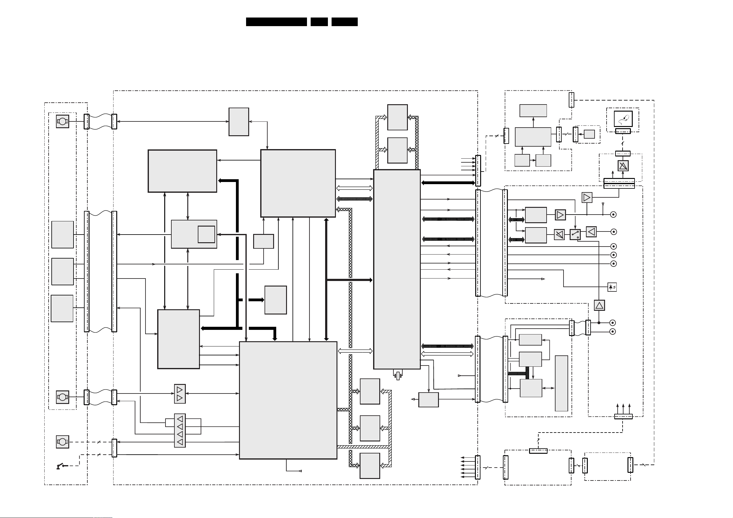
Block diagrams, Circuit diagrams and PWB’s
5. Block diagrams, Circuit diagrams and PWB’s
Blockdiagram 779
OVERALL BLOCK DIAGRAM CDR779
GB 24CDR779 5.
CDL 4009
LOADER ASSY
CDM3800
M
TURN
TABLE
LASER
&
FORWARD
SENSE
PHOTO
DIODES
RADIAL
FOCUS
M
SLEDGE
M
TRAY
TRAY
SWITCH
FLEX 11P
FLEX 30P
FLEX 10P
2 WIRES
2 WIRES
CDR MAIN BOARD
1330
DRIVE, HALL FEEDBACK
1000
IR, IW, IE
CAHF
A1LF, A2LF, B1LF, B2LF
C1LF - C4LF
RAD+, RADFOC+, FOC-
PCS PRE-AMP
NE532D
1220
SIN+, SINCOS+, COS-
1200
SL+, SL-
TR+, TR-
TRAYSW
POWER
DRIVER
BA5938FM
EFMTIM3
LO9805
EFM TIMING
GENERATOR
CONTROL
LINES
LASER
CONTROL
CONTROL
LINES
AEGER
TZA1020
ANALOG
ERROR SIGNAL
GENERATOR
FOR
RECORDABLE
7225
7240
RAD
FOCUS
SLEDGE
TRAY
7008
EFMDATA, EFMCLK, LWRT
CONTROL
LINES
7016
CONTROL
LINES
XDAC
M62364
CONTROL
LINES
7010
I2C BUS
ALPHA0
A1, A2, CALF
TLN, MIRN, FEN, REN, RE
REFSIN, SINPHI, REFCOS, COSPHI
VRA, VFO, VSL
TRAYIN, TRAYOUT
TRAYSWF
HALL
MOTOR
DRIVER
BA6856FP
7330
HIN WOBBLE
HF AMP
FILTER
I2C
EEPROM
M24C08
CDR60
SAA7392
DECODER
ENCODER
MOTOR CONTROL
OFFTRACK
LLP
CDR60PLL
7207
MACE2
SAA7399
BASIC ENGINE
PROCESSOR
ATIPSYNC
SYS-CLK-BE
(8.4672 Mhz)
7300
CONTROL
LINES
MAD0 - MAD7
MA8 - MA17
7270
ADDRESS
BUS
DOBM-CDR
SUBCODE BUS
I2S BUS 1
DATA
BUS
DSA-CDR
A1 - A20 D16 - D31
DIGITAL AUDIO
SIGNAL
PROCESSOR
7802
RAM
7208
FLASH
EPROM
7209
DEMUX
FLASH
ROM
7702
DRAM
DASP
MCF5244
33.8688 MHz
SYS-CLK-BE
(8.4672 Mhz)
ADDRESS
BUS
7703
1707
7701
7706A
DATA
BUS
SYS-RESET
I2C BUS
/2
74F74D
VDC2
VFTD
VDC1
+5V
MICPRES_INTCOPY
CL11
I2S BUS 2-DAC
I2S BUS 4-ADC
I2S BUS 3-CD
DSA-CD
SYS-RESET
DOBM-CD
SYS-CLK-8W (8.4672 Mhz)
VDC2
VFTD
VDC1
+5V
+12V
-12V
1820
1705
1708
1500
10 WIRES
FLEX 30P
FLEX 22P
11 WIRES
DISPLAY ASSY
1119
SLAVE DISPLAY
CONTROLLER
TMP87CH74F
KEYS
1401
MICPRES_INTCOPY
CL11
KILL-MAIN
1208
DECODER
SAA7324
CD PLAYER
0205
POWER SUPPLY
UNIT
1113
DISPLAY
15-BT-62GNK
EASY
JOG
I/O BOARD
7600
DAC
AD1855
7104
ADC
AD1877
7309
DAC
UDA1320
7207
uP
S87C654
7000
7103
1122
1050
7100,7102,7107
KILL
7 WIRES
0207
3 WIRES
7601
CD
DRIVE
1121
1209
0206
7401
FLEX
7P
2 WIRES
RC5
1200
7302
HEADPHONE
KILL
7103
1101
ON/OFF
STANDBY LED
1302
7102
KILL
ANALOG OUT
CDR/CD
CDR
ANALOG IN
EXTERNAL
DIGITAL IN1
EXTERNAL
DIGITAL IN2
DIGITAL OUT
CDR/CD
EXTERNAL
OPTICAL IN
7105
ANALOG OUT CD
DIG OUT CD
1400
3 WIRES
1104
HP-OUT
1101
1300
+5V+12V -8V
1400
2 WIRES
1300
CL 06532151_017.eps
241100
Page 25
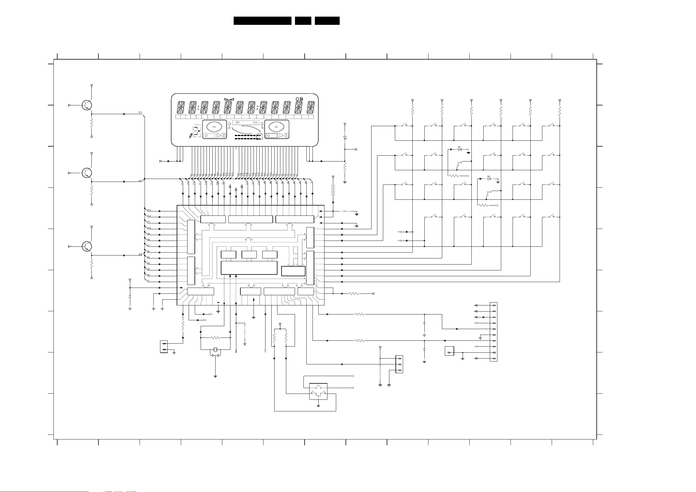
Display 779
Block diagrams, Circuit diagrams and PWB’s
GB 25CDR779 5.
123
DISPLAY BOARD - CIRCUIT DIAGRAM
A
V13
B
C
V14
D
V15
E
F
H
I
+5V
7203
BC847B
3122
82K
VFTD
+5V
7204
BC847B
3124
82K
VFTD
+5V
7100
BC847B
3106
82K
VFTD
1 11
F101
VDC2
F102
7104
TMP87CH74F
F127
F128
F129
F131
F134
F136
F139
F142
VFTD
2101
100n
TO ON/OFF &
STBY LED BOARD
F140
F143
F145
F147
F149
F174
F152
F153
GNDA
1
2
23456
1113
15-BT-60GNK
REM REC
12 34 567 8 9 10 11121314151617 181920
SYNC MANUAL
DIGITAL ||
OPTICAL||
ANALOG
1F+
2F+
3F+
47
46
45
F100
F114
65
V23
V24
66
V25
V26
67
68
V27
V28
69
V29
70
V30
71
V31
72
V32
73
V33
74
V34
75
76
V35
77
V36
VKK
78
-SCK1
79
SI1
80
SO1
GNDA
F159
F166
1
3109
560R
GNDAGNDA
1121
PH-B
45678
TIME TRACK TOTAL REM TRACK TIME FADE STEP
1G
2G
42
41
403G394G385G376G367G35
F103
F115
P03
F104
F116
V21
V20
V22
8-Bit h. break. v.
80k pull
down
8-Bit h. breakdown v.
out. port w. latch P9
source open
drain 80k p.d.
5-Bit h. breakd. v.
out w. latch PD
8-Bit Input/Output
(tri-state)
P04
P05
4
5
3
F170
F171
CDLED
F164
CD
L
R
14G2815G
10G3211G3112G3013G
33
29
V15
F106
F105
F118
V16
V15
V17
8-Bit high breakdown voltage 8-Bit high breakdown v.
output port with latch output port with latchout w. latch P8
80k pull down
VFT driver circuit (automatic display)
XIN
XOUT
VSS
8
7
9
GNDA
F162
V19
P0
P06
CDRLED
RW
8G349G
F117
V18
P07
3112
39K
1110
GNDA
RECORD
F109
F121
5051525354555657585966061626364
V9
V10
Program
Counter
-STOP
-INT0
F158
INTERRUPT
CD
RW
P9
P1016P1117P1218P1319P1420P1521P1622P1723P1824P19
15
F110
F122
F123
V6
V7
V8
8-Bit Input/Output
(tri state)
TC2
-INT1
-DV0
A
+5V
3113
10K
F167
F111
V5
8-Bit A/D
Converter
P1
TC4
3114
10K
F168
CHANGER
P21
NC
P20
27
25
26
V13
V14
F107
F108
F119
F120
V11
V12
V13
V14
P6-P9 source open drain
ROMRAM
CPU
sink open
-RESET
10 11 12 13 14 15 16 17 18 19220
RESETN
3-Bit In/Output
with latch P2
XTIN
XTOUT
F157
GNDA
2102
22n
GNDA
drain
TEST
PROG A-B
+
SHUFFLE ALL
REPEAT DISC
SCAN TRACK
P1
P2
3F-
8P39P410P511P612P713P814
6
7
3
F112
F125
F124
V4
V2
V3
P6P7
80k pull down80k pull down
4-Bit In/Output
8-Bit Input/Output
3-B. I/O P3
sink o.drain
INT4
INT2
TC1
21 22 23 24
B
54
3
1F-
2F-
1
2
F165
F113
414243444546474849
V1
V0
VDD
VAREF
VASS
AIN13
AIN12
AIN11
AIN10
(tri-state) P5
AIN7
P4
AIN6
AIN5
AIN4
AIN3
AIN2
(tri-state)
AIN1
AIN0
-SCKO
SCA
SCL
1050
MT16MT2
27
GNDA
7
40
39
38
37
36
35
34
33
32
31
30
29
28
27
26
25
F155
F161
VFTD
6100
BZX284-C3V3
VDC1
3125
3K3
+5V
GNDA
5100
BLM21
F126
2100
100n
3107
4K7
B
A
GNDA
GNDA
3108
100R
3111
100R
2111
100n
F130
F132
F135
F137
F141
F144
F146
F148
F150
F151
F154
F163
1
89
+5V
+5V
GNDA
GNDA
B
A
1
2
3
1101
PLAY /
PAUSE
1109
EVQ21
ERASE
1117
EVQ21
SCROLL
F138
F133
1122
EH-B
9
+5V
3100
4K7
SOURCE
REPEAT
2106
22p
GNDA
2104
22p
GNDA
10 11 12 13
1114
EVQ21EVQ21
REC.
START
1111
EVQ21
EXT.
1120
EVQ21
1115
EVQ21
MENU
+5V
4K7
F160
3101
F172
CD SELECT
1131-A
3115
560R
0100
1105
EVQ21
STOP
1131-B
SKHQ
CDRLED
1125
EVQ21
MODE
1118
EVQ21
CANC /
F156
INTERRUPT
1
GND WIRE
GNDA
SKHQ
DJ
DEL
RESETN
IIC_DATA
VDC2
VFTD
VDC1
IIC_CLK
+5V
3102
4K7
GNDA
GNDA
F173
CD SELECT
1130-A
3116
560R
F169
1106
EVQ21
OPEN/
CLOSE
1103
EVQ21
PROG
1130-B
SKHQ
1126
EVQ21
PLAY
1
2
3
4
5
6
7
8
9
10
SKHQ
CDLED
CD
+5V
GNDA
1119
EH-B
3103
4K7
1107
EVQ21
REC.
TYPE
1102
EVQ21
SHUFFLE
1104
EVQ21
PREV
1127
EVQ21
STOP
CD
TO MAINBORD
+5V
3104
4K7
1108
EVQ21
FINALIZE
1116
EVQ21
DISPLAY
1112
EVQ21
NEXT
1128
EVQ21
O / C
CD
+5V+5V
3105
4K7
PB DISPLAY - 4230
3104 123 4230
10
CL 06532151_002.eps
12
241100
13
0100 G10
1050 H7
1101 B9
1102 C12
1103 C11
1104 C12
1105 B10
1106 B11
1107 B12
1108 B12
A
1109 C9
1110 G4
1111 C10
1112 C12
1113 A3
1114 B10
1115 D10
1116 C12
1117 C9
1118 D10
1119 F11
1120 C10
B
1121 G3
1122 H9
1125 C10
1126 D11
1127 D12
1128 D12
1130-A D11
1130-B C11
1131-A C10
1131-B B10
2100 D7
C
2101 F2
2102 G5
2104 G10
2106 G10
2111 H8
3100 B9
3101 B10
3102 B11
3103 B11
3104 B12
3105 B13
3106 E1
D
3107 F8
3108 G8
3109 G4
3111 G8
3112 G4
3113 G6
3114 G6
3115 C10
3116 D11
3122 B1
3124 C1
3125 C8
E
5100 D7
6100 B8
7100 E1
7104 D3
7203 A1
7204 C1
F100 C3
F101 B2
F102 C2
F103 D4
F104 D4
F
F105 D4
F106 D5
F107 D5
F108 D5
F109 D5
F110 D6
F111 D6
F112 D6
F113 D7
F114 D3
F115 D4
F116 D4
GG
F117 D4
F118 D4
F119 D5
F120 D5
F121 D5
F122 D6
F123 D6
F124 D6
F125 D6
F126 D7
F127 D3
F128 D3
H
F129 D3
F130 D7
F131 D3
F132 D7
F133 E9
F134 E3
F135 E7
F136 E3
F137 E7
F138 E9
F139 E3
I
F140 E3
F141 E7
F142 E2
F143 E3
F144 E7
F145 E3
F146 E7
F147 E3
F148 E7
F149 F3
F150 F7
F151 F7
F152 F3
F153 F3
F154 F7
F155 G7
F156 G10
F157 G5
F158 G5
F159 G3
F160 G10
F161 G7
F162 G5
F163 H7
F164 G4
F165 C7
F166 G3
F167 H6
F168 H6
F169 G11
F170 G4
F171 G4
F172 B10
F173 C11
F174 F3
Page 26
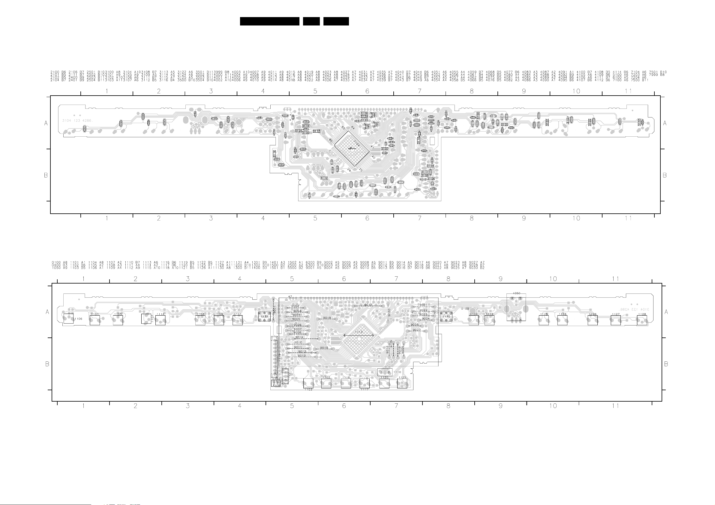
Block diagrams, Circuit diagrams and PWB’s
Display 779
DISPLAY BOARD - BOTTOM VIEW
GB 26CDR779 5.
DISPLAY BOARD - TOP VIEW
CL 06532151_003.eps
241100
Page 27
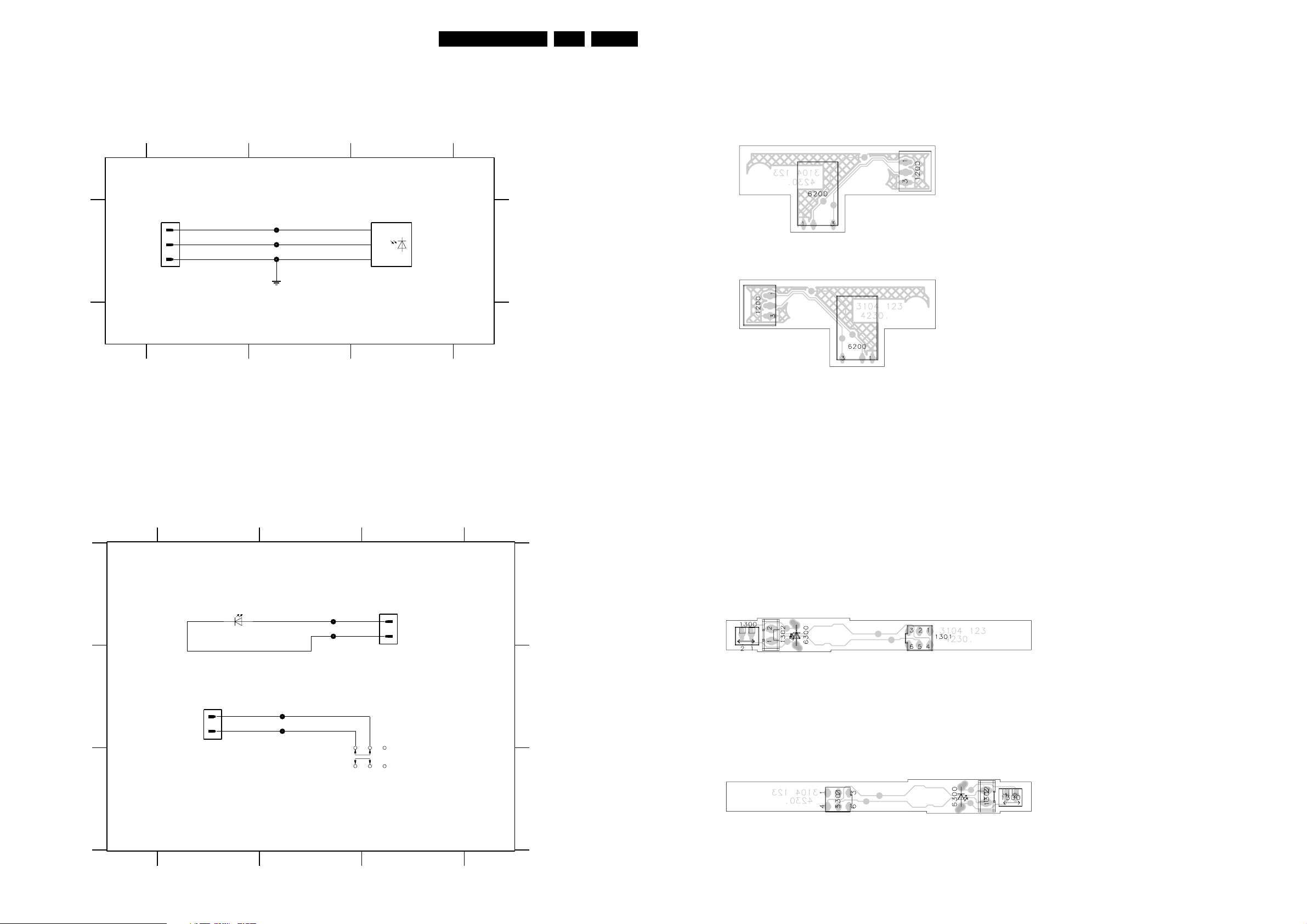
Block diagrams, Circuit diagrams and PWB’s
IR on/off
IR BOARD CDR779 - CIRCUIT DIAGRAM
123
1200 A1
6200 A3
F200 A2
F201 A2
F202 A2
GB 27CDR779 5.
IR BOARD - FRONT VIEW
1200
EH-S
AA
1
2
3
F200
F201
F202
2
VS
3
OUT
1
GND
6200
TSOP1736
IR BOARD - BACK VIEW
TO DISPLAY
BOARD
12
GNDB
3
PB DISPLAY - 4230
3104 123 4230
ON/OFF & STBY LED BOARD CDR779 - CIRCUIT DIAGRAM
123
1300 A3
1301 C3
1302 B1
6300 A1
F300 A2
A
6300
LTL-1CHPE
F300
F301
F301 A2
F302 B2
A
F303 B2
1
1300
PH-B
2
TO DISPLAY
BOARD
ON/OFF & STBY LED BOARD - FRONT VIEW
B
C
TO PSU
1302
EH-B
1
2
F302
F303
4
6
1301
SPPH23
251
3
ON/OFF & STBY LED BOARD - BACK VIEW
C
PB DISPLAY - 4230
3104 123 4230
B
CL 06532151_004.eps
241100
Page 28
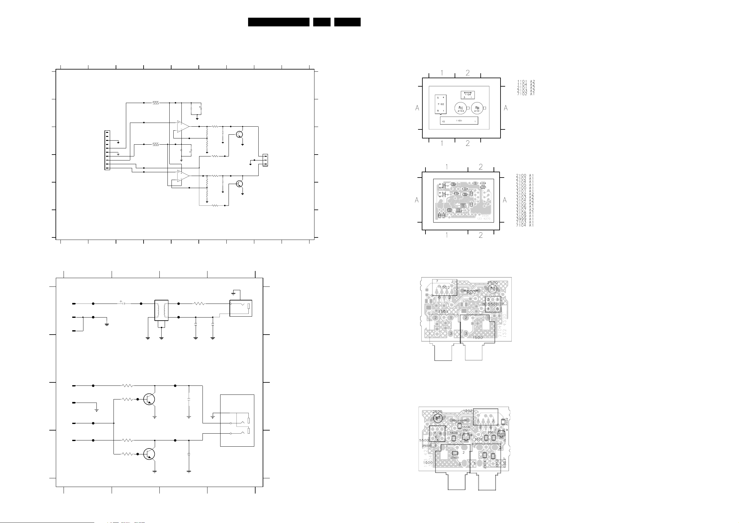
Block diagrams, Circuit diagrams and PWB’s
HPCD out
HEADPHONE BOARD - CIRCUIT DIAGRAM
1234
A
3100
F100
10R
B
F104
1101
1
PH-B
NC
2
NC
3
C
D
4
5
6
7
8
9
10
GND
NC
+12V
GND
-12V
HPRIGHT
KILL
HPLEFT
3101
F106
10R
F110
F111
E
56789
F101
7102-A
3
8
NJM4556AD
2
4
F105
F107
2102
100n
7102-B
5
8
NJM4556AD
6
4
F114
GB 28CDR779 5.
1101 C2
1104 C8
2100 B5
2101 B6
2102 C5
2103 C5
2104 C6
2105 D6
3100 B4
3101 C4
A
3102 C6
3103 C6
3104 D6
3105 E6
3106 B6
3107 D6
3108 D6
2100
2101
100n
22u
F102
1
3102
7k5
3103
10K
2103
22u
7
3104
7k5
3105
10K
F103
3106
82R
2104
1n
F108
3108
1K2
3107
82R
2105
1n
F115
3109
1K2
7103
BC818
1104
PH-B
3
F109
2
1
F113F112
7104
BC818
3109 E6
7102-A B5
7102-B D5
7103 C7
B
7104 E7
F100 B4
F101 B5
F102 B6
F103 B7
F104 B4
F105 C5
F106 C4
F107 C5
F108 D6
F109 D8
F110 D4
C
F111 D4
F112 D6
F113 D7
F114 E5
F115 E6
D
E
HEADPHONE BOARD - TOP VIEW
HEADPHONE BOARD - BOTTOM VIEW
F
CDR779 HP
3104 123 4270.2
123
456789
CD OUT BOARD - CIRCUIT DIAGRAM
12
5500
7CHA
1502-3
F500
DIGININT
52044
A
3
1502-4
F501
2500
10u
52044 4
1502-2
52044
2
B
TO CD MAIN BOARD
1502-7
7
52044
RIGHT2
1502-6
52044
C
6
F505
GNDD
3501
180R
3502
2K2
F508
GNDD
1502-1
F506
KILL
52044 1
1502-5
52044 5
LEFT2
D
F507
3503
180R
3504
2K2
F509
DIGOUTCOIL
F502
34
2
1
78
GNDD
GNDD GNDD
7500
BC847B
GNDD
7501
BC847B
34
GNDD
1
2
3
1500
YKC21-3416
DIGITAL OUT CD
ANALOG OUT CD
1501
YKC21-3613
3
2
1
6
F510
F511
F503
F504
GNDD
2503
220p
2504
220p
3500
68R
33n
2501
GNDD
GNDD
2502
33n
F
CD OUT BOARD - TOP VIEW
1500 A4
1501 C4
1502 A1
1502 A1
1502 A1
1502 C1
1502 C1
A
1502 C1
1502 D1
2500 A2
2501 A3
2502 A4
2503 C3
2504 D3
3500 A3
3501 C2
3502 C2
B
3503 D2
3504 D2
5500 A2
7500 C2
7501 D2
F500 A1
F501 A1
F502 A2
F503 A3
F504 A3
F505 C1
F506 C1
F507 D1
F508 C2
F509 D2
F510 C3
F511 D3
CD OUT BOARD - BOTTOM VIEW
C
D
GNDD GNDD
12
PB DISPLAY - 4230
3104 123 4230
34
CL 06532151_005.eps
241100
Page 29
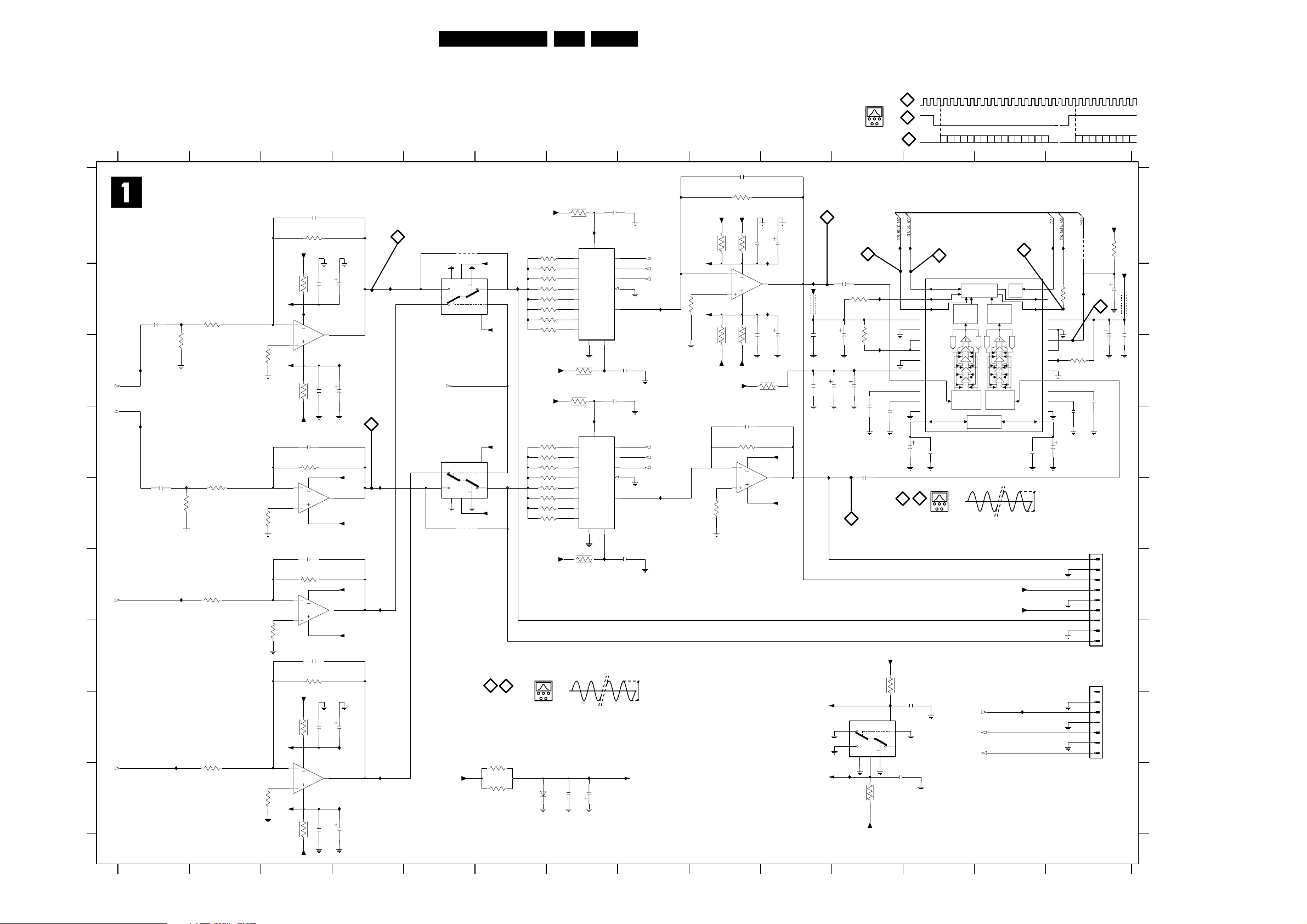
I/O board: Ext DAC
12345678910111213 14
EXT DAC
A
B
2109
100u
C
D
E
F
G
H
I
I121
CDR_RIGHTIN
CDR_LEFTIN
I125
2137
100u
CD_RIGHTOUT
CD_LEFTOUT
12345678910111213 14
I137
I116
I132
Block diagrams, Circuit diagrams and PWB’s
2102
10p
3102
51K
-9Va
2106
2107
22n
47R
OP275GS
7103-A
47R
4
OP275GS
8
7103-B
4
OP275GS
8
7105-B
10p
51K
47R
47R
1
I117
2122
22n
7
7
2145
22n
7105-A
OP275GS
1
I123
2153
22n
47u
47u
2146
47u
47u
2123
-Vaa
+Vaa
-Vab
+Vab
I134
2154
I127
3124
51K
3140
51K
3119
51K
3148
51K
51K
3137
51K
3125
10K
3143
10K
3157
10K
10K
-Vaa
+Vaa
3149
-Vab
+Vab
3111
I115
4
2
8
3
3129
+9Va
2132
10p
3134
51K
6
5
2140
10p
3147
51K
6
5
2143
3150
-9Va
3152
4
2
8
3
3158
+9Va
GB 29CDR779 5.
1,4112MHz
21
44,1KHz
20
0.5uS/DIV
2100
10p
3100
+5Va
3101
47R
14
I109
1
2
MICPRES_INTCOPY
7
8
Vss
Vee
Y1
Y0
7101-B
74HC4053D
3107
-5Vay
6
E
Vdd
16
I110
Z
15
S
10
+5Vay
3108
3109
3110
3112
3114
3117
3118
3120
+5Va
-5Vai
22K
15K
10K
6K8
4K7
3K3
2K4
1K6
13
14
15
12
1
5
2
4
3130
47R
15
22K
I128
I133
I139
7101-C
74HC4053D
Y0
5
Y1
3
8
-9Va
I129
3131
3133
3135
3136
3138
3139
3141
3144
15
+5Vay
16
Vdd
S
9
Z
4
E
Vee7Vss
6
-5Vay
3145
14
1ms/DIV
31543153
470R
3155
470R
6100
13
15K
14
10K
15
6K8
12
4K7
1
3K3
5
2K4
2
1K6
4
-5Vai
0V
SBC442 TEST CD
1kHz/-30dB
2151
22n
BZX284-C5V1
I101
Y0
Y1
Y2
Y3
Y4
Y5
Y6
Y7
3127
47R
I124
Y0
Y1
Y2
Y3
Y4
Y5
Y6
Y7
3146
47R
GND
GND
I138
16
8
16
8
VCC
VCC
47u
2152
2101
22n
7102
74HCT4051D
11
S0
10
S1
S2
E_
Z
VEE
7
I122
2124
22n
7107
74HCT4051D
11
S0
10
S1
S2
E_
Z
VEE
7
I131
9
6
3
2118
22n
9
6
3
2141
22n
LEVEL_A0
LEVEL_A1
LEVEL_A2
LEVEL_A0
LEVEL_A1
LEVEL_A2
300mVpp
-5Vai
I113
I130
-Vac
3116
10K
+Vac
I/O BOARD LAYOUT.3 - CIRCUIT DIAGRAM 1
-5Vai
3103
3121
+5Va
10K
3142
2
3
47R
47R
+5Va
6
5
10K
-9Va
3104
3122
+9Va
4
8
2129
10p
3132
10K
22n
47R
OP275GS
7100-A
2111
22n
47R
4
OP275GS
8
7100-B
2103
I107
I114
3128
4R7
16
2104
47u
+Vac
47u
-Vac
2112
I108
5100
2119
+5Vd
BLM21
2113
10n
100n
2120
I126
1
7
2108
100u
2114
21
3115
4K7
3123
4K7
4u7
I119
4u7
47u
2121
2126
2136
100u
17
+5Vay
7101-A
74HC4053D
Y0
12
Y1
13
Vee7Vss
8
I135
-5Vay
3156
-5Vai
3104 123 4249.3
19
{IIS_BCLK_ADC,IIS_WS_ADC,CL11,IIS_DATA_ADC,PST3}
I102
I111
I118
470p
2127
470p
16
+5Va
47R
3151
2144
I136
22n
16
Vdd
S
11
Z
14
E
6
2149
22n
47R
LEFT CHANNEL
I103
20
7104
AD1877
LRCK1
WCLK2
BCLK3
DVDD4 DVDD2 25
DGND15 DGND2 24
RDEDGE6 RESET_ 23
S|M_7
384|256_8
AVDD9
VINL10 VINR 19
CAPL111
CAPL212
AGNDL13 AGNDR 16
VREFL14 VREFR 15
2130
4u7
17
1ms/DIV
SERIAL OUTP
INTERFACE
3-STAGE
FIR DEC
FILTER
D
A
C
SINGLE TO
DIF INPUT
CONV
VOLTAGE
REFERENCE
2133
100n
0V
SBC442 TEST CD
1kHz/-30dB
DOBM_CD
CD_LEFTOUT
CD_RIGHTOUT
D
D
A
A
C
C
3-STAGE
FIR DEC
FILTER
SINGLE TO
DIF INPUT
CONV
CLK
DIV
D
A
C
+12Va
-12Va
I104
19
CLKIN 28
TAG 27
SOUT 26
MSBDLY_ 22
RLJUST 21
AGND 20
CAPR1 18
CAPR2 17
2134
100n
Adjustable with easy jog
via IC's 7102, 7107
I100
RIGHT CHANNEL
MSBMSB LSB
I105
3113
47R
3126
I120
4K7
2128
470p
2131
4u7
1
2
3
4
5
6
7
8
9
1
2
3
4
5
6
7
CL 06532151_006.eps
3105
I112
1100
1101
18
2125
470p
2115
PH-B
+5Vd
2155
52044
3106
4K7
+5Vd
4u7
5101
4u7
2116
241100
BLM21
10n
A
B
C
D
E
F
G
H
I
1100 F14
1101 G14
2100 A9
2101 A7
2102 A3
2103 A10
2104 A10
2106 B3
2107 B4
2108 B11
2109 B1
2111 B10
2112 B10
2113 B10
2114 C11
2115 C14
2116 C14
2118 C8
2119 C10
2120 C10
2121 C11
2122 C3
2123 C4
2124 C7
2125 C14
2126 D11
2127 D11
2128 D14
2129 D9
2130 D12
2131 D14
2132 D3
2133 D12
2134 D13
2136 D11
2137 E1
2140 F3
2141 F8
2143 G3
2144 H10
2145 H3
2146 H4
2149 I10
2151 I7
2152 I7
2153 I3
2154 I4
2155 B14
3100 A9
3101 A7
3102 A3
3103 A9
3104 A9
3105 A14
3106 A14
3107 A5
3108 A6
3109 B6
3110 B6
3111 B3
3112 B6
3113 B14
3114 B6
3115 B11
3116 B9
3117 B6
3118 B6
3119 B2
3120 B6
3121 C9
3122 C9
3123 B11
3124 B2
3125 C3
3126 C14
3127 C7
3128 C10
3129 C3
3130 C7
3131 D6
3132 D9
3133 D6
3134 D3
3135 D6
3136 D6
3137 E2
3138 E6
3139 E6
3140 E2
3141 E6
3142 E9
3143 E3
3144 E6
3145 E5
3146 F7
3147 F3
3148 F2
3149 G3
3150 G3
3151 G9
3152 H3
3153 I2
3154 I6
3155 I6
3156 I9
3157 I3
3158 I3
5100 B10
5101 B14
6100 I6
7100-A B9
7100-B E9
7101-A H9
7101-B B5
7101-C D5
7102 A8
7103-A C3
7103-B E3
7104 B12
7105-A I3
7105-B G3
7107 D8
I100 H13
I101 A7
I102 A11
I103 A12
I104 A13
I105 A14
I107 B10
I108 B10
I109 B4
I110 B6
I111 B11
I112 B14
I113 B8
I114 B10
I115 B3
I116 B1
I117 C4
I118 C11
I119 C11
I120 C14
I121 C1
I122 C7
I123 I4
I124 D7
I125 D1
I126 D10
I127 E1
I128 E4
I129 E6
I130 E8
I131 F7
I132 F1
I133 F4
I134 H4
I135 I9
I136 H10
I137 H1
I138 I7
I139 I4
Page 30
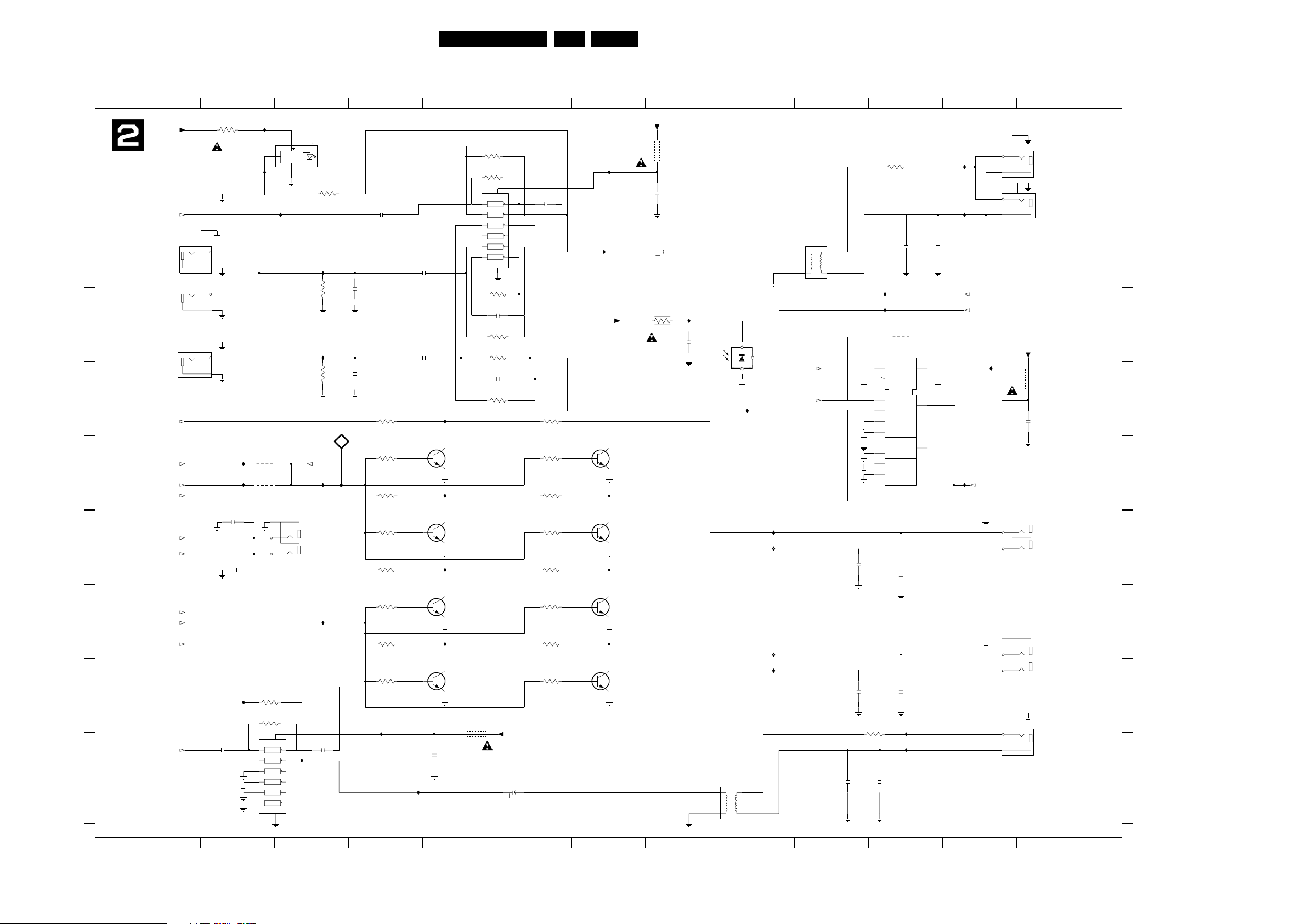
I/O board: Cinch
Block diagrams, Circuit diagrams and PWB’s
GB 30CDR779 5.
A
CINCH
B
DIG IN 1
C
DIG IN 2
D
E
F
G
H
I
3104 123 4249.3
123456789101112
+5Vd
DIG_OUT
CDR_RIGHTOUT
KILL_PSU
KILL_MAIN
CDR_LEFTOUT
CDR_RIGHTIN
CDR_LEFTIN
CD_RIGHTOUT
KILL
CD_LEFTOUT
DOBM_CD
3200
4R7
2200
33p
5
3
4
YKC21-3271
1200-B
7
8
YKC21-4079
1201-C
3
1
2
YKC21-4079
1201-B
I218
I219
2215
33p
2217
33p
CDR ANALOG IN
2222
22n
I201
7200
GP1F32T
2
1
DRIVER
I205
3
I207
-8V during play
3218
3219
3
1
2
YKC21-3342
1205-A
3233
3K3
3236
3K3
14
VCC
1A
1Y
2
1
2A
2Y
4
3
3A
3Y
6
5
4A
4Y
8
9
5A
5Y
10
11
6A136Y
12
7211
GND
74HCU04D
7
3202
I210
I214
3205
100R
3206
75R
3211
75R
2208
150p
2212
150p
2203
22n
100R
2207
22n
2211
22n
I217
1A
1
2A
3
3A
5
4A
9
5A
11
6A126Y
13
74HCU04D
7201
3K3
3204
3K3
VCC
14
GND
3207
3K3
2209
22n
3209
3K3
3210
3K3
2213
22n
3213
3K3
1Y
2Y
3Y
4Y
5Y
7
2202
2
22n
4
6
8
10
32153214
100R
I204
I209
+5Vd
1
KILL
I220
I230
2223
22n
3216
1K2
3220
100R
3223
1K2
3225
3227
1K2
3229
100R
3231
1K2
I235
I239
I223
I228
I232
2221
22n
7203
BC847B
7205
BC847B
7207
BC847B
7209
BC847B
5203
BLM21
+5Vd
2224
10u
3217
1K2
3221
100R
3224
1K2
3226
100R100R
3228
1K2
3230
100R
3232
1K2
7204
BC847B
7206
BC847B
7208
BC847B
7210
BC847B
I/O BOARD LAYOUT.3 - CIRCUIT DIAGRAM 2
+5Vd
5202
2206
10u
3208
4R7
BLM21
2201
22n
I212
2210
22n
1
6200
GP1F32R
3
IR
2
I216
5201
7CHA
34
2
1
6
78
MICPRES_INTCOPY
I224
I226
I233
I234
5200
7CHA
34
2
1
6
78
DOBM_CD
2225
33n
2216
33p
2219
33p
3235
68R
I211
I213
1
15
2
3
5
6
11
10
14
13
3203
68R
3237
7202
74HC157D
G1
EN
MUX1~
1
3222
I237
I238
2226
33n
2204
33n 33n
16
VCC
8
GND
4
7
9
12
2218
33p
2220
33p
1200-A
YKC21-3271
I203
I208
2205
I221
1
2
4
5
YKC21-4079
1201-A
DIG OUT CDR/CD
DIG_IN1
OPT_IN
I215
DIG_IN2
6
4
5
YKC21-3342
1205-B
ANALOG OUT CDR/CD
1207
YKC21-3071
3
2
1
ANALOG OUT CD
1
2
YKC21-3394
1208
13
5
6
+5Vd
5204
BLM21
2214
22n
3
DIG OUT CD
CL 06532151_007.eps
12345678910111213
241100
1200-A A12
1200-B B2
1201-A B12
1201-B D1
1201-C C1
1205-A F3
1205-B F12
1207 G12
1208 I12
2200 A2
2201 A8
2202 A6
A
2203 A4
2204 B11
2205 B12
2206 B8
2207 B5
2208 B4
2209 C6
2210 C8
2211 C5
2212 D4
2213 D6
2214 D13
2215 F2
B
2216 F11
2217 F2
2218 F11
2219 H11
2220 H11
2221 I5
2222 I2
2223 I3
2224 I6
2225 I10
2226 I11
3200 A2
C
3202 A5
3203 A11
3204 A5
3205 A3
3206 B3
3207 C6
3208 C8
3209 C6
3210 C6
3211 D3
3213 D6
D
3214 D4
3215 D6
3216 E4
3217 E6
3218 E2
3219 E2
3220 E4
3221 E6
3222 E11
3223 F4
3224 F6
3225 F4
E
3226 F6
3227 G4
3228 G6
3229 G4
3230 G6
3231 H4
3232 H6
3233 H2
3235 H11
3236 H2
3237 C11
5200 B10
F
5201 I9
5202 A8
5203 H5
5204 D13
6200 C9
7200 A3
7201 B5
7202 C11
7203 E5
7204 E7
7205 F5
G
7206 F7
7207 G5
7208 G7
7209 H5
7210 H7
7211 I3
I201 A2
I203 A12
I204 A7
I205 A2
I207 A3
I208 A12
H
I209 B7
I210 B3
I211 C11
I212 C8
I213 C11
I214 C3
I215 D12
I216 D9
I217 D5
I218 E2
I219 E2
I220 E3
I221 E12
I
I223 E5
I224 F9
I226 F9
I228 F5
I230 G3
I232 G5
I233 G9
I234 H9
I235 H4
I237 H11
I238 I11
I239 I4
Page 31
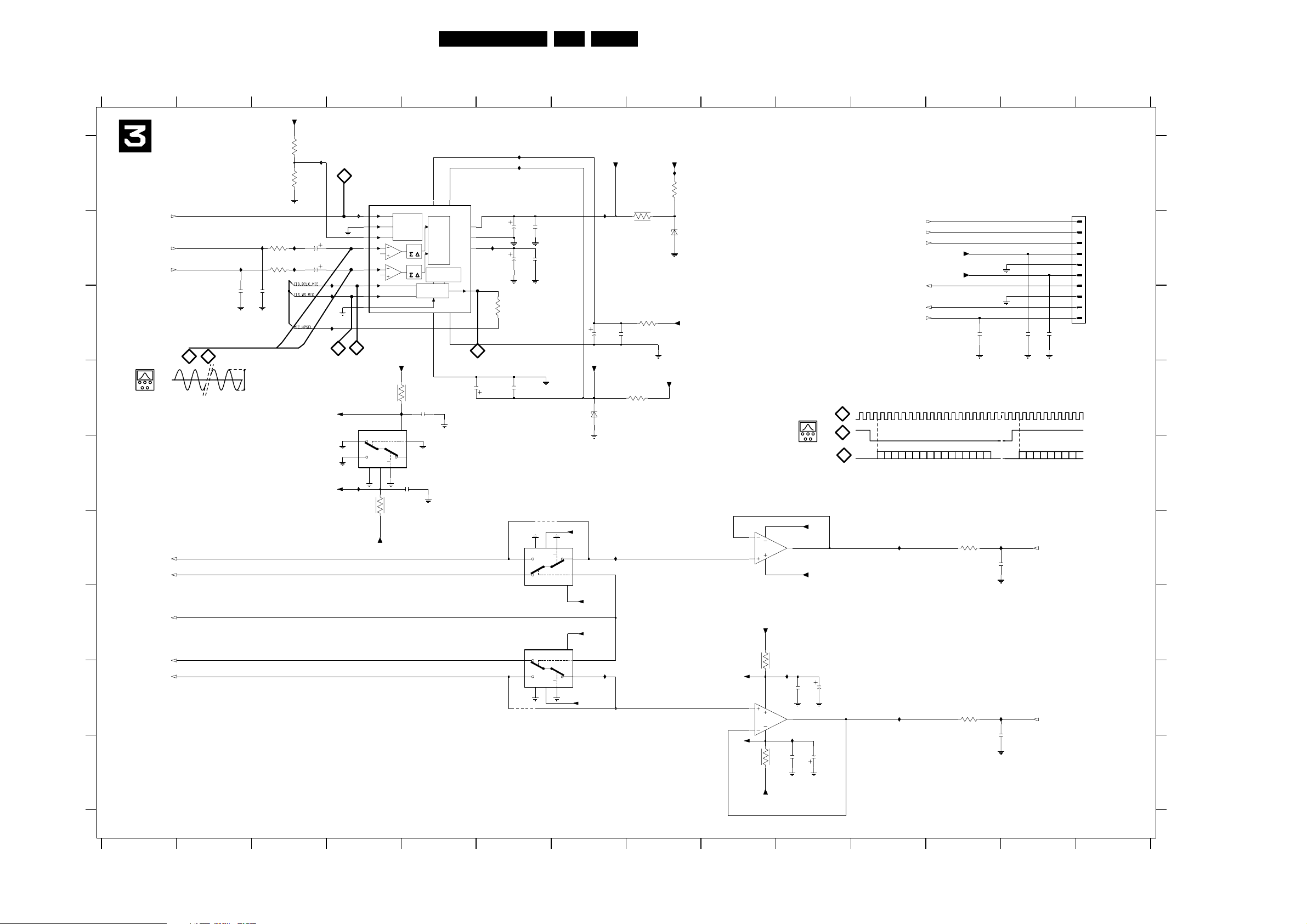
Block diagrams, Circuit diagrams and PWB’s
I/O board: Mic ADC
GB 31CDR779 5.
1
A
B
MIC ADC
CL11_MIC
MIC_LEFTIN
MIC_RIGHTIN
2
I311
1n
2308
C
23
24
0V
D
1ms/DIV
SBC442 TEST CD
1kHz/-30dB
Adjustable with
pot 3109 on
headphone & mic
board
E
F
CDR_RIGHTOUT
CD_RIGHTOUT
G
MIC_HPSEL
CD_LEFTOUT
CDR_LEFTOUT
H
HP SELECT
3 4 5 6 7 8 9 10 11 12 13 14
+3V3d
3300
47K
3301
47K
I309
I308
3305
12K
I312
3307
12K
1n
2325
{MIC_HPSEL,IIS_WS_MIC,IIS_BCLK_MIC}
2304
47u
2307
47u
I301
I315
22
I313
I316
25
+5Vax
-5Vax
11.2896MHz
7300
UDA1360TS
I304
8 SYSCLK
14 FSEL
7 PWON
1 VINL
3 VINR
BCK
11
12 WS
6 SFOR
26
7301-A
74HC4053D
Y0
12
Y1
13
Vee7Vss
E
8
6
I317
47R
3317
-5Vai
CLOCK
CONTROL
ADC
ADC
+5Va
47R
3313
I318
16
Vdd
S
11
Z
14
2316
22n
16
VDDA9VDDD
DC-CANCEL
FILTER
DIGITAL
INTERFACE
VSSD
10
2313
22n
FILTER
DECIMATION
VSSA
15
5VREFP
4VREFN
2VREF
13DATAO
27
2311
47u
I310
3310
47R
I300
I302
2301
47u
2305
47u
2312
100n
Y1
1
Y0
2
74HC4053D
74HC4053D
Y0
5
Y1
3
3321
7301-B
7301-C
8
2302
100n
2306
100n
3318
7
Vee8Vss
Vee7Vss
+3V3a
I306
2310
2309
100n
47u
+3V3d
3314
100R
6301
UDZ-3.3B
-5Vax
6
E
Z
15
S
10
Vdd
16
16
Vdd
S
9
Z
4
E
6
I322
+5Vax
+5Vax
I325
-5Vax
3304
47R
3311
1R
+5Vd
+5Va
I303
3302
82R
6300
UDZ-3.3B
+3V3a
+Vad
-Vad
HP_LEFTOUT
KILL
HP_RIGHTOUT
MIC_RIGHTIN
MIC_LEFTIN
MICPRES_INTCOPY
1,4112MHz
26
44,1KHz
25
0.5uS/DIV
4
6
5
+9Va
3
2
3320
3322
8
47R
8
4
47R
OP275GS
7302-B
I326
7302-A
OP275GS
I328
7
2317
22n
1
2319
22n
-Vad
+Vad
2320
47u
47u
27
2318
LEFT CHANNEL
I320
I327
-9Va
+9Va
3323
1K
3324
1K
2300
100p
I323
2321
I324
2322
2326
RIGHT CHANNEL
MSBMSB LSB
1n
1n
100n
2327
HP_RIGHTOUT
HP_LEFTOUT
100n
1300
PH-B
1
2
3
4
5
6
7
8
9
10
TO HEADPHONE & MIC BOARD
I
1300 B13
2300 C12
2301 B6
2302 B6
2304 B3
2305 B6
2306 B6
2307 B3
2308 C2
2309 C7
2310 C8
2311 D6
2312 D6
A
2313 D5
2316 E5
2317 H10
2318 H10
2319 I10
2320 I10
2321 F12
2322 I12
2325 C3
2326 C13
2327 C13
3300 A3
B
3301 A3
3302 A8
3304 A8
3305 B3
3307 B3
3310 C6
3311 C8
3313 D4
3314 D8
3317 E4
3318 F6
C
3320 H9
3321 H6
3322 I9
3323 F12
3324 H12
6300 B8
6301 D7
7300 A4
7301-A D4
7301-B G6
7301-C G6
7302-A H9
D
7302-B F9
I300 A6
I301 A3
I302 A6
I303 A8
I304 A4
I306 A7
I308 B3
I309 B3
I310 B6
I311 B2
I312 B3
E
I313 B4
I315 C4
I316 C4
I317 E4
I318 D5
I320 F11
I322 F7
I323 F13
I324 H13
I325 H7
I326 H10
F
I327 H11
I328 H10
G
H
I
-9Va
3104 123 4249.3
I/O BOARD LATOUT.3 - CIRCUIT DIAGRAM
CL 06532151_008.eps
1234567891011121314
241100
Page 32
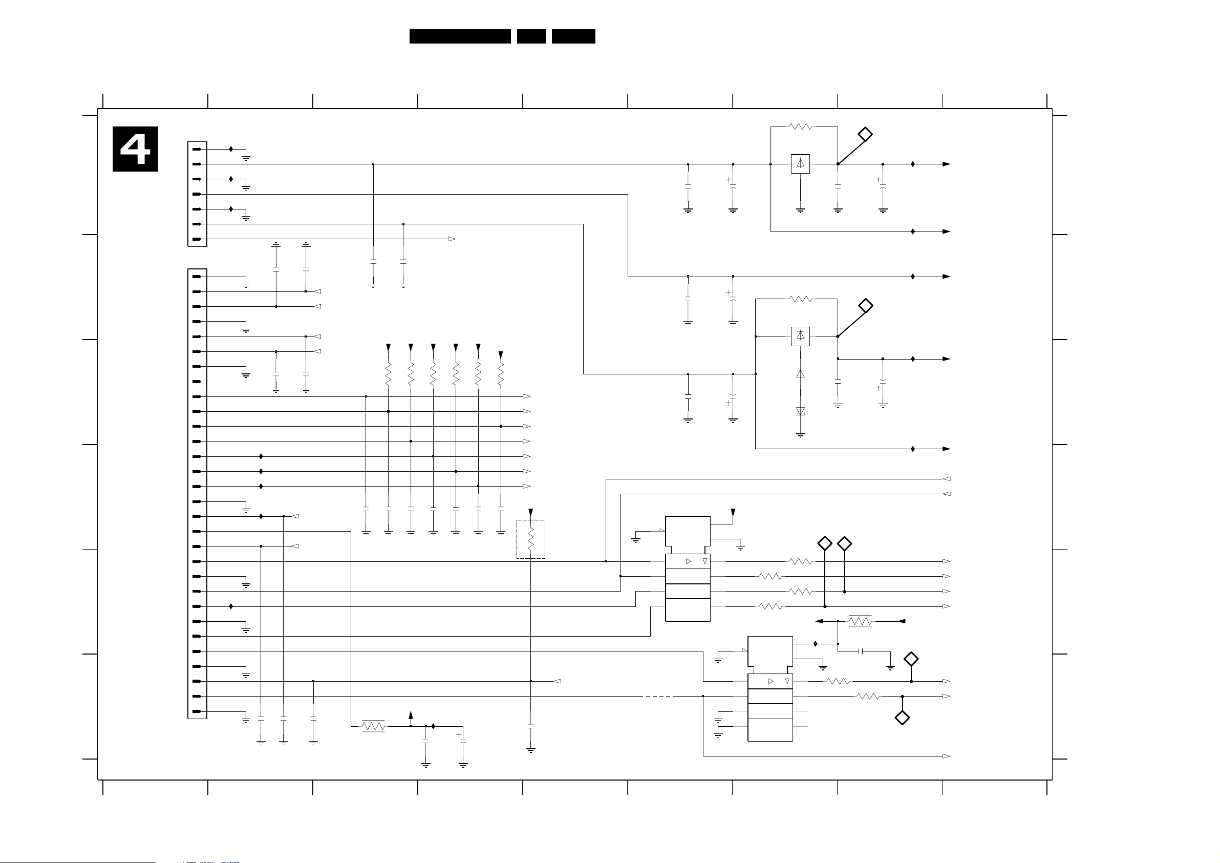
Block diagrams, Circuit diagrams and PWB’s
I/O board: Power supply
GB 32CDR779 5.
A
B
C
D
E
F
123456789
POWER SUPPLY
1400
EH-B
TO PSU
TO CDR MAIN
BOARD
1401
1
2
3
4
5
6
7
1
2
3
4
5
6
7
8
9
10
11
12
13
14
15
16
17
18
19
20
21
22
23
24
25
26
27
28
29
30
3104 123 4249.3
I404
I405
I411
I413
I407
I408
I409
I410
2423
2413
2415
100p
100p
100p
2424
100p
2414
2416
100p
PST3
IIS_DATA_ADC
2429
100p
OPT_IN
DIG_OUT
DIG_IN2
DIG_IN1
22n
2428
100n
100n
2427
+5Vd +5Vd +5Vd +5Vd +5Vd
10K
10K
3404
2417
3411
4R7
3403
100p
2418
100p
+5Vd
2419
100p
I412
2410
3405
2420
100n
10K
3406
100p
KILL_PSU
2421
2411
10K
3407
100p
2422
47u
+5Vd
10K
3408
100p
2425
10K
+5Vd
100p
3412
2426
18
16
14
12
2401
2405
2407
+5Vdx
4u7
100u
4u7
7403-B
74HC244D
19
11
13
15
17
3414
47R
3416
47R
EN
KILL_MAIN
DEEMP
MUTE
MICPRES_INTCOPY
LEVEL_A2
LEVEL_A1
LEVEL_A0
10K
OPTION
MIC_HPSEL
22n
1
2
4
6
8
4400
2400
2404
2406
7403-A
74HC244D
EN
GND
Vcc
100n
100n
100n
20
10
I/O BOARD LAYOUT.3 - CIRCUIT DIAGRAM 4
3400
0R0
7400
L78M09
1
3
IN
OUT
GND
2
2402
3401
0R0
7401
MC7905
2
3
IN
OUT
GND
1
6401
BAS216
2408
6400
BZX284-C3V9
5
3413
47R
3415
47R
+5Vdx +5Vd
I414
20
Vcc
10
GND
3418
9
7
5
3
47R
3
100n
2
100n
6
3417
4R7
2412
100n
3419
47R
2403
2409
I400
47u
I401
I402
I403
47u
I406
7
4
11.2896MHz
+9Va
+12Va
+5Va
-9Va
-12Va
IIS_BCLK_MIC
IIS_WS_MIC
IIS_BCLK_ADC
IIS_WS_ADC
IIS_DATA_DAC
IIS_BCLK_DAC
IIS_WS_DAC
CL11
CL11_MIC
CL 06532151_009.eps
241100
A
B
C
D
E
F
1400 A1
1401 B1
2400 A6
2401 A6
2402 A7
2403 A8
2404 B6
2405 B6
2406 C6
2407 C6
2408 C7
2409 C8
2410 F4
2411 F4
2412 E8
2413 B2
2414 B2
2415 C2
2416 C2
2417 D3
2418 D3
2419 D3
2420 D4
2421 D4
2422 D4
2423 F2
2424 F2
2425 D4
2426 F5
2427 B3
2428 B3
2429 F2
3400 A7
3401 B7
3403 C3
3404 C3
3405 C4
3406 C4
3407 C4
3408 C4
3411 F3
3412 D5
3413 E7
3414 E7
3415 E7
3416 E7
3417 E8
3418 F8
3419 F8
4400 F6
6400 C7
6401 C7
7400 A7
7401 B7
7403-A D6
7403-B E7
I400 A8
I401 A8
I402 B8
I403 C8
I404 A2
I405 A2
I406 C8
I407 D2
I408 D2
I409 D2
I410 D2
I411 A2
I412 F4
I413 E2
I414 E7
12345
6789
Page 33
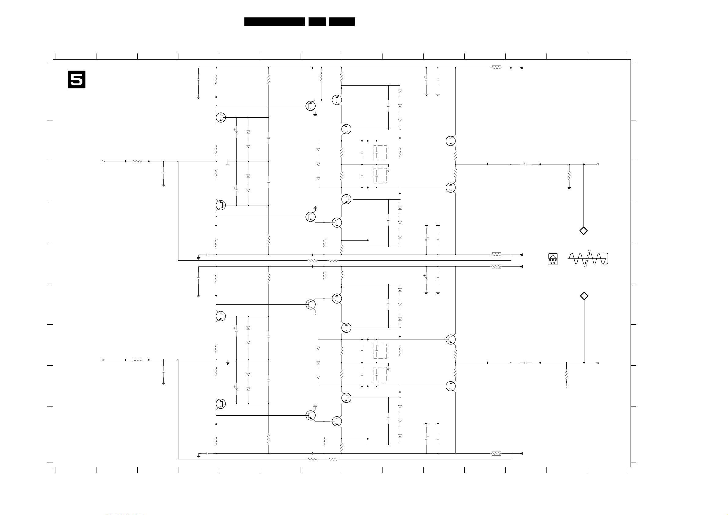
Block diagrams, Circuit diagrams and PWB’s
I/O board: DAC filter
1234567891011121314
DAC FILTER_L
A
I/O BOARD LAYOUT.3 - CIRCUIT DIAGRAM 5
B
I514I513
FILTER_L
C
D
E
F
3508
2K
68n
2520
DAC FILTER_R
G
H
I
3104 123 4249.3
FILTER_R
I547
3530
2K
I548
68n
2521
2500
22n
2510
22n
7501
BC848B
BC858B
7508
2509
22n
7511
BC848B
BC858B
7518
2519
22n
330R
330R
330R
330R
3501
1K2
I503
3504
I529
3518
1K2
3523
1K2
I537
3526
I563
3540
1K2
3516
3538
2526
2528
2530
2532
GB 33CDR779 5.
2500 A4
7518 H4
2501 A10
7519 I8
2502 A10
7520 A7
2503 B8
I500
BC858B
BC848B
1K
3549
68R
1K
BC858B
BC848B
1K
3550
68R
7502
7507
7512
7517
3503
150R
I504
BC858B
7500
3505
3K3
3511
3K3
7509
BC848B
3519
150R
3525
150R
I538
BC858B
7510
3527
3K3
3533
3K3
7519
BC848B
3541
150R
I509
2503
270p
2506
270p
I523
I543
2513
270p
2516
270p
I557
I531
I565
2522
390p
2523
390p
2524
390p
2525
390p
2534
OPTION
OPTION
2535
2536
OPTION
OPTION
2537
100n
100n
100n
100n
6501
BAS216
6503
BAS216
6504
BAS216
I507
3506
12K
I524
6508
BAS216
6510
BAS216
6511
BAS216
6514
BAS216
6516
BAS216
6517
BAS216
I541
3528
12K
I558
6521
BAS216
6523
BAS216
6524
BAS216
2501
100u
2507
100u
2511
100u
100u
2517
2502
22n
2508
22n
2512
22n
2518
22n
7503
BC848B
3507
68R
3513
68R
BC858B
7505
7513
BC848B
3529
68R
3535
68R
BC858B
7515
I515
I549
3502
2K2
6500
BAS216
47u
100n
2527
6502
BAS216
6509
BAS216
2529
2531
2533
3517
2K2
3524
2K2
3539
2K2
100n
100n
100n
6512
BAS216
47u
6513
BAS216
47u
6515
BAS216
6522
BAS216
6525
BAS216
47u
I532
3521
1K8
I535
I566
3543
1K8
3545
BC858B
7520
6505
BAS216
6506
BAS216
6507
BAS216
7521
BC848B
BC858B
7522
6518
BAS216
6519
BAS216
6520
BAS216
7523
BC848B
1K
3546
3547
3548
3500
2R2
3520
2R2
3522
2R2
3542
2R2
I501
+9Va
2504
100u
-9Va
+9Va
2514
100u
-9Va
I516
1ms/DIV
I550
10K
3512
10
0V
SBC442 TEST CD
1kHz/-30dB
11
10K
3534
CL 06532151_010.eps
A
B
CDR_LEFTOUT
C
D
320mVpp
E
F
G
CDR_RIGHTOUT
H
I
241100
2504 C12
2506 C8
2507 D10
2508 D10
2509 E4
2510 E4
2511 E10
2512 E10
2513 G8
2514 G12
2516 H8
2517 I10
2518 I10
2519 I4
2520 C3
2521 H3
2522 B8
2523 C8
2524 G8
2525 H8
2526 B5
2527 B6
2528 C5
2529 C6
2530 G5
2531 G6
2532 H5
2533 H6
2534 A9
2535 D9
2536 F9
2537 I9
3500 A11
3501 A5
3502 A6
3503 A8
3504 B5
3505 B8
3506 B9
3507 B10
3508 B2
3511 C8
3512 C13
3513 C10
3516 C4
3517 D6
3518 D5
3519 E8
3520 E11
3521 E7
3522 E11
3523 E5
3524 E6
3525 E8
3526 G5
3527 G8
3528 G9
3529 G10
3530 G2
3533 H8
3534 H13
3535 H10
3538 H4
3539 I6
3540 I5
3541 I8
3542 I11
3543 I7
3545 A7
3546 E7
3547 E7
3548 I7
3549 E7
3550 I7
6500 B5
6501 A9
6502 B5
6503 A9
6504 A9
6505 B7
6506 C7
6507 C7
6508 D9
6509 C5
6510 D9
6511 D9
6512 C5
6513 G5
6514 F9
6515 G5
6516 F9
6517 F9
6518 G7
6519 G7
6520 H7
6521 H9
6522 H5
6523 I9
6524 I9
6525 H5
7500 A8
7501 A4
7502 B7
7503 B10
7505 C10
7507 C7
7508 D4
7509 D8
7510 F8
7511 F4
7512 G7
7513 G10
7515 H10
7517 H7
7521 D7
7522 F7
7523 I7
I500 A7
I501 A12
I503 A5
I504 A8
I507 B9
I509 B8
I513 B2
I514 B3
I515 B11
I516 B12
I523 C8
I524 C9
I529 D5
I531 D8
I532 E7
I535 E7
I537 F5
I538 F8
I541 G9
I543 G8
I547 G2
I548 G3
I549 G11
I550 G12
I557 H8
I558 H9
I563 I5
I565 I8
I566 I7
12
3456789
10 11 12 13 14
Page 34
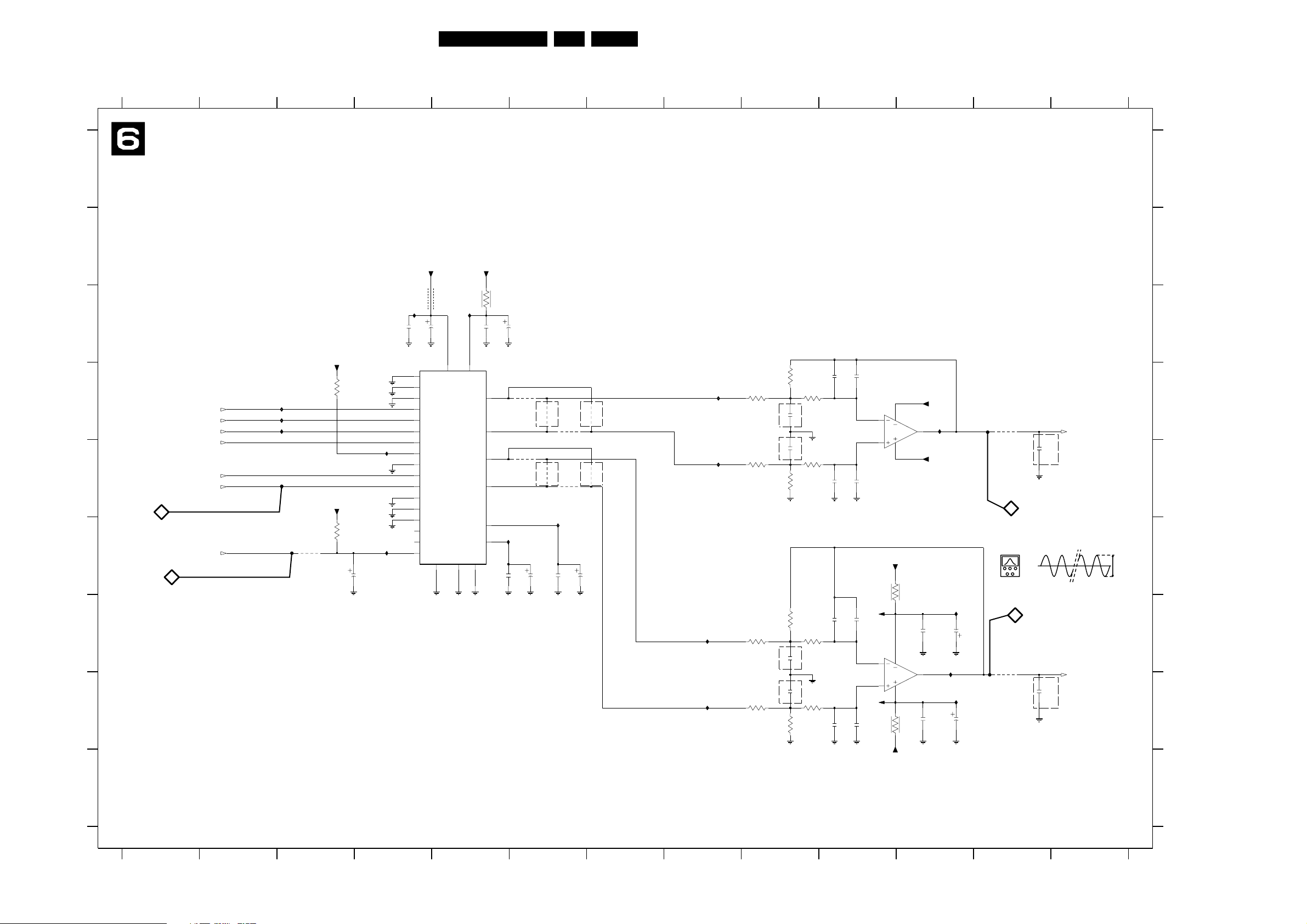
I/O board: DAC
Block diagrams, Circuit diagrams and PWB’s
GB 34CDR779 5.
1234
5 6 7 8 9 10 11 12 13
DAC
A
B
+5Vd
5600
BLM21
I605
C
+5Vd
10K
3603
D
E
IIS_DATA_DAC
IIS_WS_DAC
IIS_BCLK_DAC
CL11
DEEMP
MUTE
12
F
PST3
13
I604
I602
I603
I600
3601
+5Vd
3602
1K
2626
4u7
I608
I606
2601
10
6
7
27
25
26
2
21
20
9
23
3
4
5
8
22
24
100n
2600
7600
AD1855
96|48_
384|256_
X2MCLK
SDATA
L|RCLK_
BCLK
MCLK
IDPM0
IDPM1
DEEMP
MUTE
CLATCH
CCLK
CDATA
ZEROR
ZEROL
PD|RST_
DGND
150u
DVDD
1
G
H
I617
28
18
AVDD
OUTL+
OUTL-
OUTR+
OUTR-
FILTR
FILTB
AGND115AGND2
11
+5Va
3607
2612
2R2
2611
150u
100n
2K4
3604
3621
17
OPTION
3622
3626
3623
3627
16
3625
12
OPTION
13
3624
3628
OPTION
OPTION
I607
I610
3605
1K8
3609
1K8
OPTION
OPTION
2603
2604
3611
3606
1K8
1n
1n
3610
1K8
2K4
2602
2606
330p
330p
2622
2623
220p
220p
-Vaf
4
2
8
3
1
OP275GS
7601-A
I609
+Vaf
3608
2605
10n
OPTION
FILTER_L
8
2610
10u
I616
2607
100n
2608
10u
I612
I615
3614
1K8
3617
1K8
OPTION
OPTION
3613
2616
2617
3619
2K4
1n
1n
2K4
3615
1K8
3618
1K8
2613
2621
330p
330p
2624
2625
-Vaf
220p
+Vaf
220p
-9Va
2R2
3612
I611
I613
I614
2615
2620
47u
47u
2614
100n
4
6
7
OP275GS
8
5
7601-B
2619
100n
2R2
3620
1ms/DIV
9
3616
0V
SBC442 TEST CD
1kHz/-30dB
FILTER_R
2618
10n
OPTION
350mVpp
14
I601
19
100n
2609
2600 C4
2601 C4
2602 D10
2603 D9
2604 E9
2605 E12
2606 E10
2607 F6
2608 F6
2609 F5
2610 F6
2611 C5
A
2612 C5
2613 G10
2614 G11
2615 G11
2616 G9
2617 H9
2618 H12
2619 H11
2620 H11
2621 H10
2622 D10
2623 E10
B
2624 G10
2625 H10
2626 F3
3601 F3
3602 F3
3603 D3
3604 D9
3605 D9
3606 D9
3607 C5
3608 D12
C
3609 E9
3610 E9
3611 E9
3612 F10
3613 G9
3614 G9
3615 G9
3616 G12
3617 H9
3618 H9
3619 H9
3620 H10
D
3621 D6
3622 D6
3623 D6
3624 D7
3625 E6
3626 E6
3627 E6
3628 E7
5600 C4
7600 D4
7601-A E11
7601-B H11
E
I600 E3
I601 F5
I602 D3
I603 D3
I604 D3
I605 C4
I606 F4
I607 D8
I608 E4
I609 D11
I610 E8
F
I611 G11
I612 G8
I613 G11
I614 H11
I615 H8
I616 F6
I617 C5
G
H
+9Va
I
3104 123 4249.3
1
I/O BOARD LAYOUT.3 - CIRCUIT DIAGRAM 6
2345678910111213
CL 06532151_011.eps
241100
I
Page 35
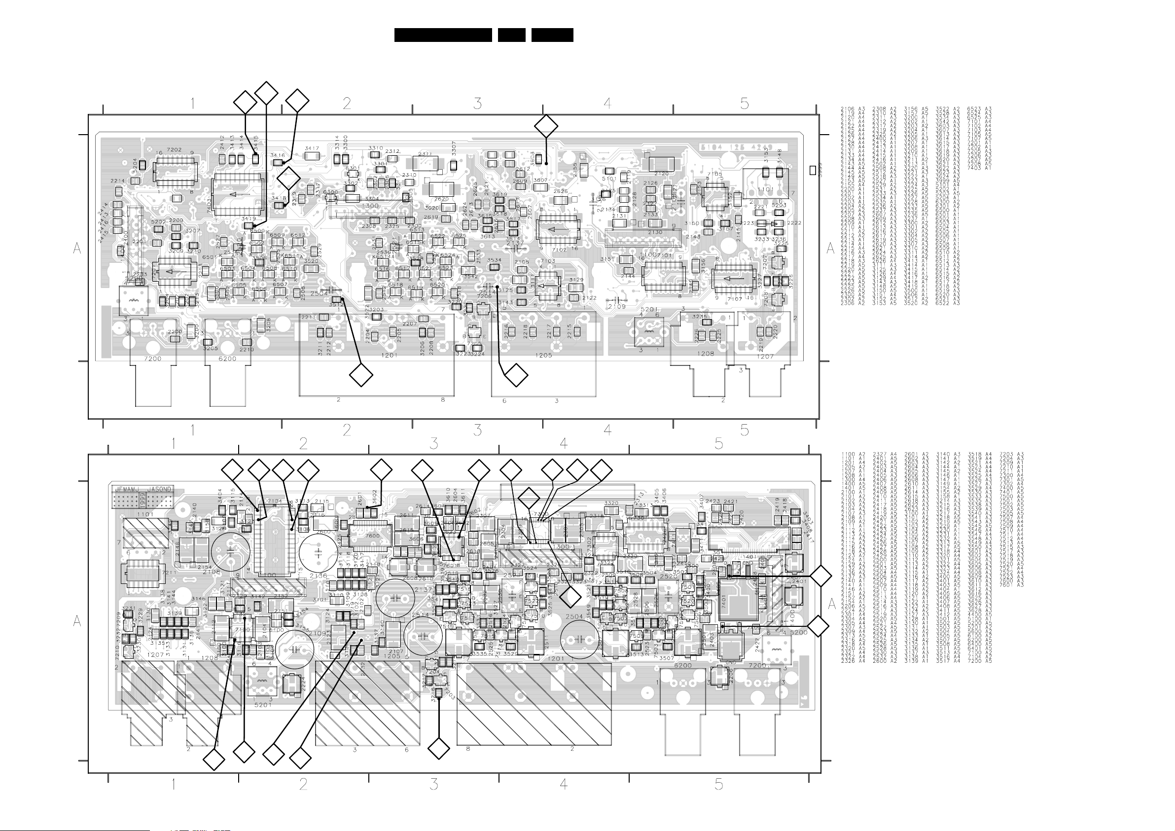
Layout I/O board
Block diagrams, Circuit diagrams and PWB’s
GB 35CDR779 5.
6
I/O BOARD LAYOUT.3 - BOTTOM VIEW
4
5
12
7
10
11
I/O BOARD LAYOUT.3
- TOP VIEW
20
21
19
18
13
27
89
23
25
26
24
2
22
3
16
17
14
15
1
CL 06532151_012.eps
241100
Page 36
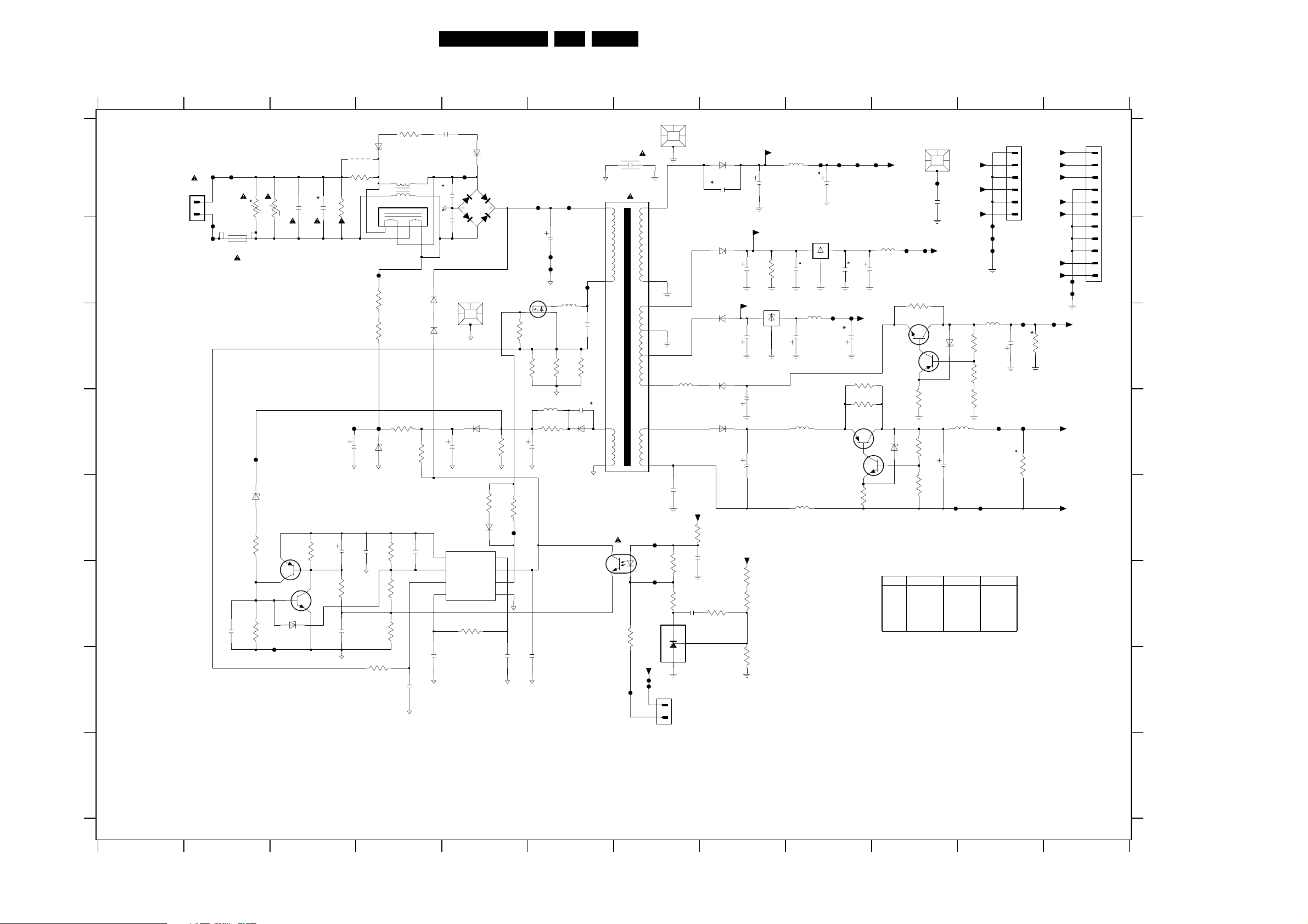
PSU CDR3-ECU
Block diagrams, Circuit diagrams and PWB’s
GB 36CDR779 5.
123456789101112
POWER SUPPLY UNIT CDR3-ECO
F100
F103
1
2
F101
F102
1120
T2.0A H 250V
2150
100n
3120
6141
3142
BC857B
3150
2322593
V
F121
UDZ-20B
10R
7141
1K5
F122
V
3119
6150
UDZ-4.7B
G
A
B
C
D
E
F
H
0101
HCS0528
2120
220n
3141
7150
BC847B
2119
10K
3117
F109
2141
3151
2106
0101 A2
0125 B5
0205 A12
0206 G7
A
B
C
D
G
H
0207 A11
0208 A10
0260 A7
1120 B2
2102 G4
2104 E4
2106 F3
2109 G4
2111 G5
2119 A3
2120 A3
2121 B6
2125 A5
2126 B5
2127 C6
2128 A5
2129 D3
2130 D6
2131 A7
2133 D5
2134 D5
2141 E3
2142 E4
2150 F2
2161 G5
2201 E7
2202 F7
2210 A8
2213 A9
2220 D8
2221 E7
2222 D10
2230 B8
2231 B9
2232 B9
2234 B9
2240 C8
2242 C9
2243 C9
2250 D8
2252 C11
2253 A8
2260 A10
3102 F5
3103 E5
3104 E4
3105 F4
3106 F4
3109 G4
3110 D5
3111 D4
3112 D6
3113 E5
3117 A3
E
3119 B3
3120 A2
3122 A4
3123 B4
3124 A4
3125 C5
3126 C6
3127 C6
3128 C6
3129 D4
3134 C4
3141 E3
F
3142 E2
3150 F2
3151 F3
3201 E7
3202 F8
3203 F7
3204 F8
3205 F8
3206 G8
3207 F7
3208 F7
3220 D11
3221 E10
3222 D10
3223 E9
3224 D9
3225 C9
3229 C11
3230 B8
3232 C11
3233 D11
3234 D10
3235 B10
3236 C11
5120 A4
5121 A4
5125 B6
5130 D6
5131 A6
5210 A9
5220 D11
3124
470R
6100
9122
F108
F125
4u7
2142
BZX79-C15
UF1922P4
12
43
5120
5121
CU15D3
3
4
18K
3123
18K
3134
3129
6129
BZX84-C24
3104
100n
3105
3106
3109
1K
10K
15K
15K
1K
2109
3122
2R7
680K
2129
T
2u2
56K
4n7
1
2104
2
3111
330p
2128
33n
F104
2125
43
2126
0125
HEATSINK
6106
1N4006
6107
1N4006
2134
68R
7110
UC3842A
1n
1
COMP
2
Vfb
3
Isense6OUTPUT
4
RtCt
1n8
2102
2n2
2n2
1SS355
100u
3102
22K
6101
1
6102
2
6130
BZX79-C15
S1NB80
3103
6133
Vref
VCC
GND
3110
33R
1SS355
8
7
5
2161
STP3NB60FP
10K
3125
3126
10K
2133
3113
270R
F110
2111
100n
5131
F111
2127
3128
2130
6132
BYD33D
CQY80NG
1R5
7131
CT283D3
2
5
470p
7
9
F219
F105
F106
2121
100u
F107
F112
7125
5125
83R
1R
1R
3127
5130
68u
3112
22R
100u
100n
: Reserved Item Number
*
HEATSINK
2131
2n2
3203
100R
-8Vr
0260
F215
F216
17
15
11
13
10
14
16
18
F217
F218
1
2
0206
2221
3207
3208
5255
1
2
EH-B
1u
47n
1K
470R
2202
22n
+12Vr
3
BYW98-200
BYD33D
BYD33J
BYD33D
10R
3201
2201
100n
3204
10K
7201
TL431CLP
6210
SB360
2253
6230
6240
6250
6220
2230
-8Vr
2240
2250
2220
+5Vr
3202
3205
3206
2210
+12Vr
1m
L7908
IN2OUT
220u
100u
330u
3K3
220R
3K3
2m2
3230
7249
GND
+5Vr
1
0205
1
2
3
4
5
6
7
8
9
10
11
F213
F214
VFTD
VDC2
VDC1
CL 06532151_013.eps
EH-B
241100
F220
F221
F222
F212
5250
10u
12K
5K6
470R
F210
USA
Reserved
CU15D3
Jumper
1
2
3
4
5
6
0207
2252
F207
10u
F209
3220
EH-B
VDC2
VFTD
VDC1
+5V
+5V
+12V
-8V
F208
3236
0208
F224
F223
F202
F201
5210
6u8
2213
7260
1IN3
OUT
GND
2231
5225
5226
4u7
4u7
5240
10u
100u
2
F205
2232
F206
2243
BC327-25
7254
BC847B
2234
3225
68R
3224
68R
7253
3223
1K
3
2242
+5V
F230
F204
F203
5230
2u2
22u
should be YK type
3235
-8V
390R
3K3
7251
BC337-40
7252
BC857B
3K3
3234
3222
6202
2121 100u 220u
3122
5120
5121
9122
0101 Unpolarized
1K2
UDZ-2.7B
1K2
3221
Euro WW
47u
Reserved
UF1922P
Reserved
Jumper
+12V
+5V
10n
2260
2222
-8V
+12V
6201
3232
UDZ-22B
3229
3233
5220
10u
100u
F211
2R7
Reserved Reserved
CU15D3
Reserved
Unpolarized Polarized
5225 D9
5226 E9
5230 B10
5240 C9
5250 C11
5255 C7
6100 A4
6101 A5
6102 A5
6106 B4
6107 C4
6129 D4
6130 D5
6132 D6
6133 E5
6141 E2
6150 F3
6201 C10
6202 D10
6210 A8
6220 D8
6230 B8
6240 C8
6250 C8
7110 E5
7125 B6
7131 F6
7141 F3
7150 F3
7201 G7
7249 B8
7251 C10
7252 C10
7253 D9
7254 D9
7260 B9
9122 A4
F100 A2
F101 A2
F102 B2
F103 B2
F104 A5
F105 A6
F106 A6
F107 B6
F108 B4
F109 D3
F110 E5
F111 B6
F112 B6
F121 D2
F122 F3
F125 D4
F201 A9
F202 A9
F203 B10
F204 B10
F205 C9
F206 C9
F207 C11
F208 C12
F209 D11
F210 D11
F211 E10
F212 E11
F213 B12
F214 B12
F215 E7
F216 F7
F217 G7
F218 G7
F219 G7
F220 B11
F221 B11
F222 B11
F223 A9
F224 A10
F230 A10
12
3456789101112
Page 37
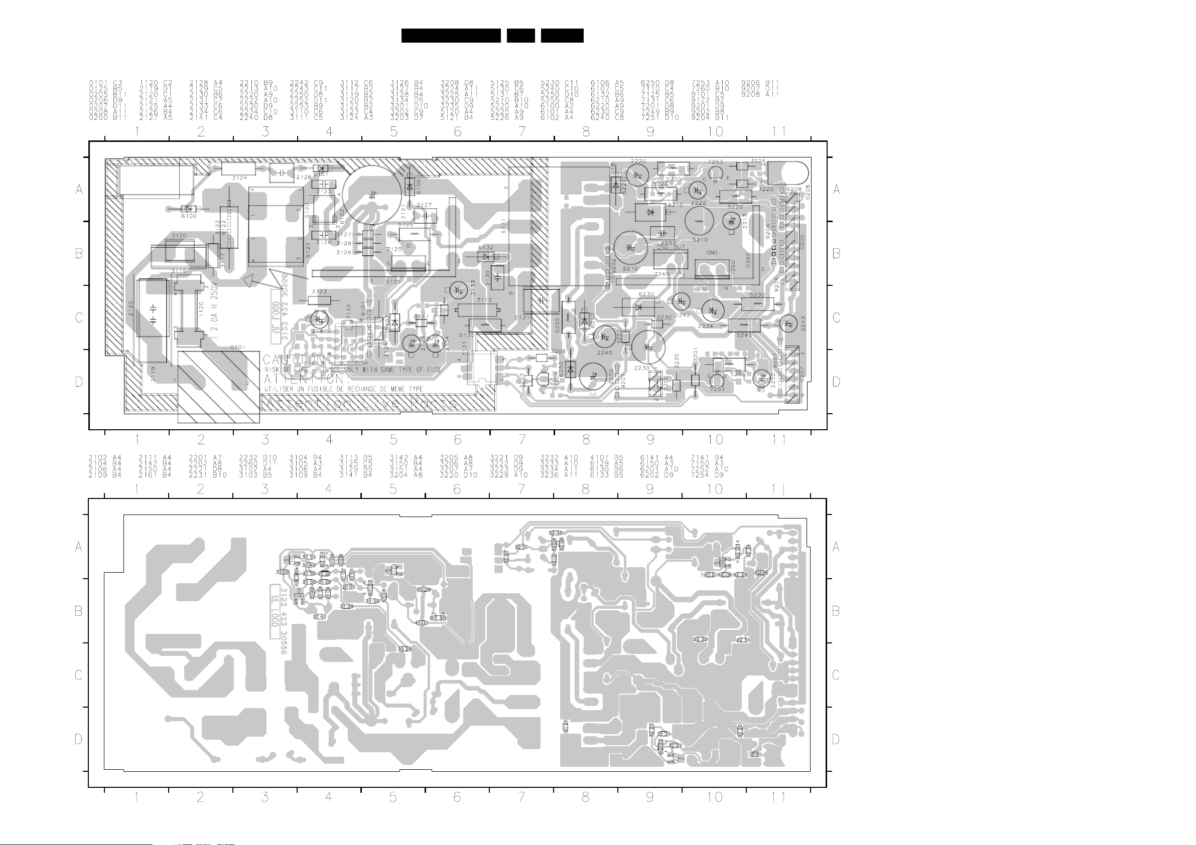
Block diagrams, Circuit diagrams and PWB’s
Layout PSU CDR3-ECO
POWER SUPPLY UNIT CDR3-ECO - TOP VIEW
GB 37CDR779 5.
POWER SUPPLY UNIT CDR3-ECO - BOTTOM VIEW
CL 06532151_014.eps
241100
Page 38
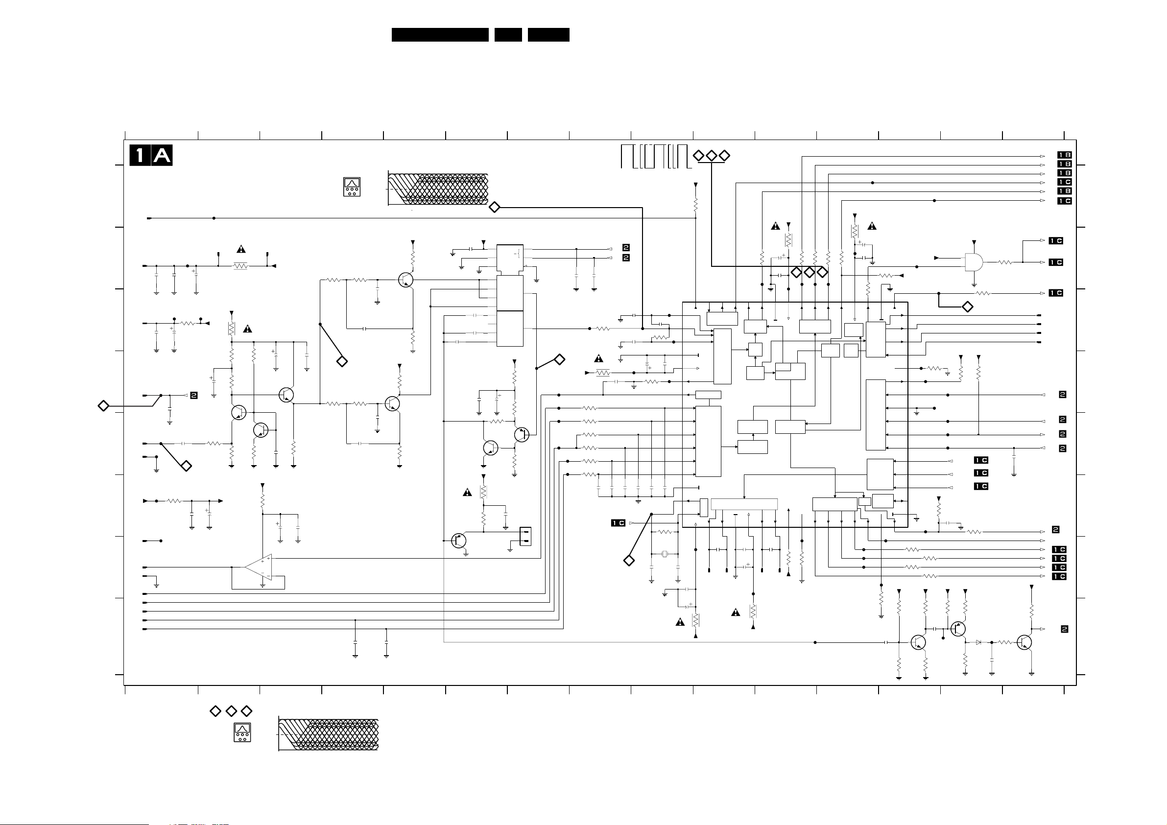
Block diagrams, Circuit diagrams and PWB’s
CD main board: Decoder & servo processor part
1000-1 C1
1000-11 G1
1000-12 D1
1000-2 E1
1000-3 B1
1000-4 E1
1000-5 A1
1000-6 H1
1000-7 H1
1000-8 H1
1000-9 H1
1003 F7
1004 G9
1009 C15
1010 C15
1011 C15
1012 C15
1021 G10
1022 G11
1023 G11
1028 B2
1029 B3
1050-1 G1
1050-2 G1
2128 B12
2130 B6
2131 B12
2132 B11
2133 B1
2134 B1
2135 B1
2137 B8
2138 B8
2139 B11
2140 C4
2141 C6
2142 C9
2143 C4
2145 C9
2146 C6
2147 C1
2148 C1
2149 C6
2150 C9
2151 D3
2152 D3
2155 D9
2156 D2
2157 D8
2159 D1
2160 D6
2161 D6
2162 E4
2163 E1
2166 E3
2167 E14
2168 F8
2170 F81000-10 G1
2172 F9
2173 F9
2174 F1
2175 F2
2178 G10
2182 F3
2183 F3
2184 G9
2185 G9
2186 G10
2189 G9
2191 H9
2200 H4
2201 H4
2230 H14
2232 H131020 G10
2236 F6
2280 F14
2285 G10
2286 G11
3160 A9
3161 B12
3162 B11
3164 B15
3169 B5
3171 B13
3172 B11
3174 B4
3177 C2
GB 38CDR779 5.
3178 C8
3179 C1
3180 C5
3181 C9
3182 D2
3183 D2
3184 D8
3185 D14
3186 D14
3187 D2
3188 D5
3189 D7
3190 D9
3191 D4
3192 D42154 D9
3194 D8
3195 E8
3196 E6
3197 E8
3198 E2
3199 E3
3200 E8
3201 E22164 E4
3203 E5
3204 E8
3205 E72169 F8
3208 F12171 F9
3212 F9
3213 F3
3214 F14
3219-A G13
3219-B G13
3219-C G13
3219-D G13
3220 G11
3225 H10
3229 H9
3265 H15
3266 H14
3267 H13
3268 H14
3269 H14
3270 H152233 H13
3274 B12
3275 B12
3276 B11
3279 B2
3280 F13
3281 F6
3282 G11
3283 G123168 B12
3285 H13
3286 H13
3287 H133173 B4
7000 C93176 C14
7006 D3
7007 E7
7008 E2
7009 D5
7010 E6
7011 E2
7023 B5
7024 F6
7025 B7
7130 H15
7131 H14
7132 H13
7311-A G2
F139 A12
F143 A13
F146 A23193 D7
F147 B1
F149 B13
F151 C13
F154 C1
F155 C2
F156 C8
F157 C3
F159 C9
F160 D13202 E2
F162 D7
F163 D14
F164 D7
F165 D133206 E8
F166 E7
F167 E143211 F6
F168 E14
F170 E1
F171 E7
F172 E14
F173 E1
F174 E7
F175 E7
F177 F1
F178 F9
F180 G1
F181 F13
F182 G13
F183 G12
F184 G11
F190 H14
F191 H11
F192 H143273 B11
F302 B12
F303 B11
F304 B11
F305 B11
F306 B12
F308 B11
F309 C9
F310 C9
F311 D133284 D13
F312 D9
F313 D7
F314 D9
F315 D136003 H14
F318 G12
F319 G97005-B B14
F321 G12
F322 G12
F324 G10
A
B
C
D
CD-DA, CD-R : 5V
CD-RW : 0V
8
F
G
H
12345
CD MAIN BOARD - CIRCUIT DIAGRAM 1A
DECODER & SERVO PROCESSOR PART
CONN. 1000 : TO CDM VAM1250
F147
100n
3179
4u7
RW
HFGND
HFGND
1K
1
2174
2135
F155
22u
22n
HFGND
F146
1028
+5VHF
2156
HFGND
3198
47R
2175
1
1
+5VHF
47u
7008
BFS20
HFGND HFGND
+5VHF
47u
LDON
1000-5
5
VDD
1000-3
3
2133
HFGND
VSUB
1000-1
1
2147
HFGND
F160
RW
1000-12
12
RF
F170
1000-4
4
HFGND
F173
1000-2
2
HFGND
F177
+5V
F180
FTC
1000-11
11
1
1050-1
2
1050-2
1000-10
10
1000-9
9
1000-8
8
1000-7
7
1000-6
6
PB CD MAIN 4236
CDR99
3104 123 4236
2134
470n
HFGND
F154
2148
470n
HFGND
47n
2159
HFGND
2163
33n
3208
4R7
12345
3279
3177
3182
3187
3201
TDA1308T
2
1R
1R
390R
390R
7011
BFS20
1K2
7311-A
1
3183
3202
10K
22K
+5VHF
100R
8
4
1029
1
2151
HFGND
2166
3213
2182
3
2
+5VHF
47u
47n
6789101112 15
4
6
5
eyepattern
2.5V
0,5us/DIV
3173
3174
430R
430R
2140
HFGND
2
2164
180p
2201
HFGND
2143
330p
3192
430R
2162
HFGND
1n5
F157
100n
2152
HFGND
7006
BFS20
3191
430R
1K5
3199
HFGNDHFGND
10u
2183
100n
180p
100p
2200
HFGND
+5VHF
3188
3203
560p
7009
BFS20
HFGND
>800mVpp
+5VHF
2K7
3169
7023
BFS20
2K7
3180
HFGND
2K7
2K7
HFGND
HFGND
390p
2149
680p
BF824
7024
HFGND
2130
100n
HFGND
2141
2n2
2146
1n5
BC848B
HFGND
7010
+5VHF
22n
3281
3211
16
7
8
1
5
2
4
12
14
15
11
2160
HFGND
HFGND
+12V
1K
3
74HCT4052D
VCC
VEE
GND
0
1
2
3
+5VHF
47u
1K
3196
BC858B
2R2
2236
HFGND
HFGND
2161
7007
7025
10
0
0
4x
9
3
1
6
G4
22n
22n
HFGND
3
13
HFGND
2137
HFGND
F156
9
3189
3193
3205
100n
1003
1
2
F313
390R
180R
10K
F162
F164
F166
F171
F174
F175
+3V3
3194
10K
3195
10K
3197
10K
3200
10K
3204
10K
3206
10K
PULSE DENSITY MODULATION
S1
S2
2138
2142
3178
3184
2R2
2168
22n
HFGND
220p
HFGND
HFGND
100n
2157
2169
220p
HFGND
2170
F310
2150
47n
F312
220p
2171
HFGND
CRIN
1K
7
8.4672MHz
47u
220p
3190
30K
2172
F178
33p
2184
47p
2145
3181
22K
2155
2154
2173
220p
3212
1M
1004
CX-5F
8M4672
HFGND
F309
F314
F159
100n
220p
7000
SAA7324
LDON
1
HFREF
2
HFIN
3
ISLICE
4
VSSA1
5
VDDA1
6
IREF
7
VRIN
8
D1
9
D2
10
D3
11
D4
12
R1
R2
13
VSSA2
14
15
CROUT
CRIN
16
33p
2185
2189
100n
2191
47u
+5VHF
3160
VDDA2
F319
3229
10K
63
64
V1
VERSATILE
INTERFACE
VREF GEN.
ADC
TIMING
LN19LP
17
18
1
1020
2R2
+3V3
FRONT
END
2285
1n5
V5
V4
61V462
CONTROL
CONTROL
FUNCTION
PRE-
PROCESSING
BITSTREAM DAC
VNEG21VPOS
20
2178
100n
2186
1
47u
1021
+3V3
60
MOTO2
MOTOR
DIG.
PLL
EFM
DEMOD
F324
3225
3172
F303
59
MOTO1
22RN23
1
1022
2R2
100R
VSSD3
RP
2286
1n5
+3V3
2R2
3162
2132
3273
3276
100R
47u
2139
100n
58
ADDR
PROCESSOR
1
100R
6
4
5
F305
F304
F308
57
56
55
SL
FO
VDDD2C
OUTPUT
STAGES
ERROR
CORR.
SRAM
AUDIO
SER. DATA
INTERFACE
SELPLL
TEST1
CL16
25 31
26
24
F184
10K
10K
3220
3282
1023
+3V3
F191
3274
F306
RA
DATA
F139
+3V3
2R2
3161
2128
47u
2131
F302
3275
100R
100R
100n
3168
100R
51
53
54
52
CFLG
DOEM
VDDD1P
EBU
INTERF.
PEAK
SUBCODE
DET.
SER. DATA
LOOPBACK
INTERF.
VERSAT.
KILL
WCLK
SCLK
EF
28
29
27
30
F318
F321
F322
13 14
3171
+5V
10K
50
49
CL11|4
48
SBSY
VSSD2
PROCESSOR
INTERFACE
MICROCONTROLLER
INTERF.
TEST2
F183
3283
SFSY
SUB
RCK
TEST3
STATUS
SILD
RAB
SCL
SDA
RESETn
SCLI
SDI
WCLI
V2|V3
VSSD1
KILL
32
F182
+5VHF +5VHF
10K
3286
2232
100n
3287
HFGND
47
46
45
44
43
42
41
40
39
38
37
36
35
34
33
3219-D
47R
3219-B
47R
150K
47K
F149
F311
F315
F181
3285
3267
HFGND
F143
+5V
3284
F165
3219-C
47R
3219-A
47R
2233
7132
BC848B
F151
0R
VPROC
3280
4K7
1n5
1K
F163
F167
F168
F172
10K
2280
100n
+5VHF
3268
F190
7005-B
74HCT08D
4
5
+5V
3185
SCLK_IN
DATA_IN
WCLK_IN
+5VHF
3269
100K
1K
HFGND
+5VY
14
7
3176
100R
10
11.2896MHz
+5V
4K7
3186
3214
0R
100R
BC858B
7131
6003
BAS216
3266
HFGND
4K7
6
F192
2230
4n7
3164
47R
3265
100K
2167
DOBM5_CD
DOBM5_CD
100n
+5VHF
HFGND
3270
7130
BC848B
SL
FO
RA
V4
MOT1
CFLG
A
B
CL11
1009
1
1010
1
1011
1
1012
1
C
D
SILD
SCL
SDA
RESET
EE
F
MUTE
EF
SCLK
WCLK
DATA
CL16
10K
HFDET
G
H
13 14 156789101112
9
eyepattern
2.5V
0,5us/DIV
CL 96532086_015.eps
080999
Page 39
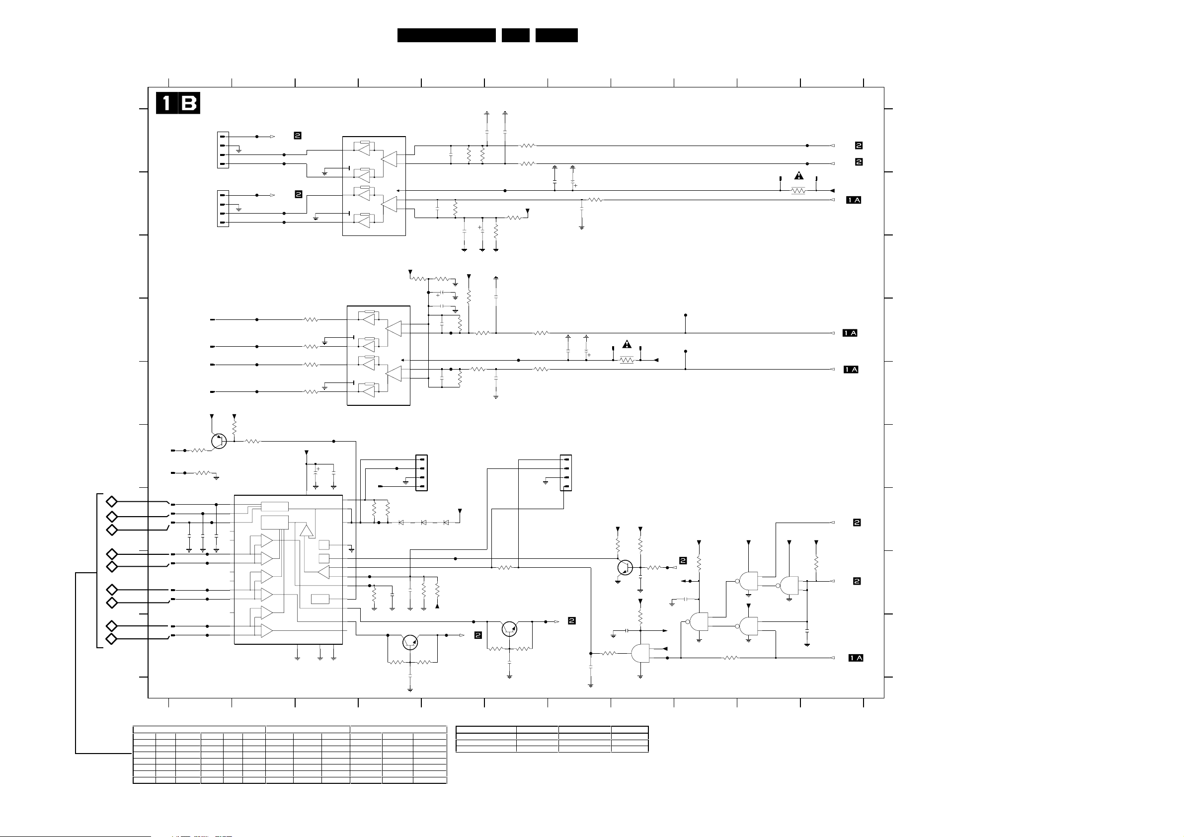
Block diagrams, Circuit diagrams and PWB’s
CD main board: Servo drivers part
123456
CD MAIN BOARD - CIRCUIT DIAGRAM 1B
SERVO DRIVERS PART
1002
A
TO TRAY
SWITCH
& MOTOR
B
TO SLEDGE
SWITCH
HOMESW
SGND
TRAY+
TRAY-
HOMESW
SGND
SL-
SL+
1001
& MOTOR
C
RAD+
1000-15
WCOIL
VCOIL
UCOIL
2113
V+
V-
W+
W-
1000-16
1000-14
1000-13
BC858B
7019
3102
47R
3117
F114
100n
PGND
47R
RAD-
2112
F124
F125
F129
F132
FOC-
FOC+
+5V
F116
PGND
F120
F123
15
16
14
13
PGND
F113
100n
2111
PGND
D
TO CDM
VAM1250
E
1006-1
F101
1
F
11
12
G
13
14
15
H
16
17
18
19
I
HALL+
F106
5
HALL-
1006-5
1006-11
11
1006-10
10
9
1006-9
1006-6
U+
6
U-
8
1006-8
1006-4
4
7
1006-7
1006-3
3
2
1006-2
TO TURN TABLE
MOTOR
PB CD MAIN 4236
CDR99
3104 123 4236
1
100n
F103
PH-B
1
2
SGND
3
4
PH-B
1
2
SGND
3
4
+5V
22K
3100
7020
3
A3
5
A2
A1
7
1
NC1
2
NC2
9
H1+
10
H1-
4
NC3
6
NC4
11
H2+
12
H2-
15
NC5
13
H3+
14
H3-
3101
22K
F112
F133
F136
F138
F145
DRIVER
GAIN
CONTROL
+
-
+
-
+
-
+
-
+
-
+
-
TRAYSW
F107
F109
HOMESW
F115
F117
234567891011
GND
+5V
VCC
8
PGND
SGND
3148
0R
3152
0R
3155
0R
3159
0R
47u
PGND PGND
25
-+
H BIAS
MT1
5V8
16
SGND
14
13
5V8
5V8
12
10
5V8
5V8
SGND
5V8
5V8
SGND
5V8
F100
100n
2105
BA6856FB
RNF
VM2
VM1
REV
REV
PS
PS
EC
+
ECR
-
CNF
VH
FG1
FG2
FG3
MT2
29 30
PGNDPGND
TDA7073A
3
4
9
TDA7073A
16
3
14
13
12
4
10
9
2104
28
27
26
24
23
22
21
20
19
18
17
16
PGND
F300
F301
F118
100K
PGND
1008
1
1R
3135
3146
F131
VDD
PGND
100n
PGND
7021
-
+
+
-
1V6
1V6
VDD
F104
1R
3134
6002
BYG50D
2119
3107
560R
15
11
+3V3
7022
-
+
+
-
PH-B
100n
PGND
7031
BC847B
10n
1
2
5
6
7
8
1
2
15
11
6
7
1
2
3
4
5V
5V
1V6
1V6
3142
270R
5
1V6
1V6
8
1005
6001
BYG50D
2118
PGND
3106
180R
2282
47K
F128
3144
2109
3145
270R
2120
2121
100n
BYG50D
47K
+5V
22u
2122
2126
6000
3143
F130
22n
F135
F140
2103
12n
10n
F119
3136
+12V
1n
3149
3158
1K2
100n
+3V3
3114
3147
1K
1K2
T2
F127
2115
8K2
150K
3156
12K
2116
3150
12K
3115
2100
4K7
22u
100n
270R
2123
2127
3105
560R
2102
F111
3138
330p
330p
3140
0R
7030
BC847B
10n
100n
3137
270R
F137
3104
180R
2281
3103
47K
3116
47K
+3V3
3151
12K
3157
12K
GB 39CDR779 5.
SGND
PGND
F126
789
SGND
47u
100n
2106
SGND
1
2
3
4
1321
2107
3132
22K
2110
100n
F134
RA
SGND
47u
2125
100n
2124
PH-B
BC848B
T1
F121
3139
10K
22n
2117
1024
7301
3113
1025
1
1
3154
1R
+5V+5V
1K
10K
3110
3130
10K
2220
100n
+5V
3278
100R
2114
100n
7005-D
14
74HCT08D
12
11
13
7
F141
+12V
FO
+5V
F108
F122
+5VX
+5VY
+5V
STBY
2108
100n
F110
6
100R
7110-B
14
74HCT00D
7
3277
10 11
F102
F105
1026
1
3131
+5VX +5V
14
11
7
MOT1
1R
7110-D
74HCT00D
12
13
100n
SL
+5VX
7110-C
14
74HCT00D
9
8
10
7
+5VX
3141
0R
7110-A
74HCT00D
14
1
3
2
7
4
5
1027
10K
TRAYIN
TRAYOUT
1
+12V
SL
RA
FO
MOT_UP
3129
MOT_SW
2221
MOT1
1000-13 E1
1000-14 E1
1000-15 D1
1000-16 D1
1001 B1
1002 A1
1005 F5
1006-1 F1
1006-10 G1
1006-11 G1
1006-2 I1
1006-3 I1
1006-4 H1
A
1006-5 F1
1006-6 G1
1006-7 H1
1006-8 H1
1006-9 G1
1008 F4
1024 D8
1025 D8
1026 B10
1027 B11
1321 F7
B
2100 A5
2102 A6
2103 A5
2104 F3
2105 F3
2106 B7
2107 B7
2108 H9
2109 B5
2110 B7
2111 G1
2112 G1
C
2113 G1
2114 I8
2115 B5
2116 B5
2117 I7
2118 H4
2119 H4
2120 C5
2121 D5
2122 D5
2123 C6
2124 D7
D
2125 D7
2126 E5
2127 E6
2220 H8
2221 I11
2281 I6
2282 I4
3100 F1
3101 F2
3102 F1
3103 A6
E
3104 I6
3105 I6
3106 I5
3107 I4
3110 G8
3113 G8
3114 A5
3115 A5
3116 A6
3117 F1
3129 H11
3130 H8
F
3131 B10
3132 B7
3134 G4
3135 G4
3136 B5
3137 B6
3138 B6
3139 I7
3140 H6
3141 I9
3142 C4
3143 H5
G
3144 H5
3145 C5
3146 H4
3147 C5
3148 D3
3149 D5
3150 D5
3151 D6
3152 D3
3154 D8
3155 E3
H
3156 E5
3157 E6
3158 E5
3159 E3
3277 H9
3278 I8
6000 G5
6001 G5
6002 G4
7005-D I8
7019 F1
7020 G2
I
7021 A4
7022 D4
7030 H6
7031 I4
7110-A H10
7110-B H9
7110-C H10
7110-D H11
7301 H8
F100 F3
F101 F1
F102 A11
F103 A2
F104 F4
F105 A11
F106 F1
F107 A2
F108 H8
F109 A2
F110 H9
F111 B6
F112 B2
F113 G1
F114 G1
F115 B2
F116 G1
F117 B2
F118 G4
F119 H5
F120 H1
F121 I7
F122 I8
F123 H1
F124 H1
F125 H1
F126 I6
F127 I5
F128 C5
F129 I1
F130 I5
F131 I4
F132 I1
F133 D2
F134 D9
F135 D5
F136 D2
F137 D6
F138 D2
F140 E5
F141 D9
F145 E2
F300 H4
F301 H4
Input conditions conn 1006 pin Outputs conn 1006 Test points on driver
684 732 9 10 11 18 17 16
U+ U- V+ V- W+ W- UCOIL VCOIL W COIL HALL_U HALL_V HALL_W
L M H M M M 6V 0V 0V 0V 5V
H M L M M M 0V 6V 6V 5V 0V
M M L M H M 0V 6V 0V 0V 5V
M M H M L M 6V 0V 6V 5V 0V
H M M M L M 0V 0V 6V 5V 0V
L M M M H M 6V 6V 0V 0V 5V
Input voltage Level Tolerance Unit
H2.80.1V
M2.50.1V
L2.20.1V
CL 96532086_016.eps
080999
Page 40
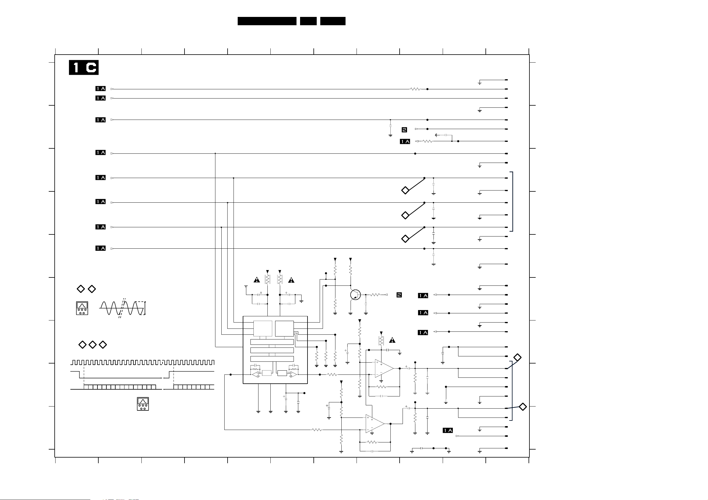
Block diagrams, Circuit diagrams and PWB’s
CD main board: Audio part
1234567
CD MAIN BOARD - CIRCUIT DIAGRAM 1C
AUDIO PART
A
B
C
D
E
G
H
F
I
23
24
0V
2ms/DIV
20 21 22
2,1168MHz
SCL
44,1KHz
WCLK
LEFT CHANNEL
DATA
PB CD MAIN 4236
CDR99
3104 123 4236
1234567891011
V4
CFLG
DOBM5_CD
CL11
SCLK
WCLK
DATA
CL16
GENERAL PURPOSE TEST
TRACK 10 1KHz 0dB
0.5uS/DIV
5Vpp
32
RIGHT CHANNEL
MSBMSB LSB
F194
DATA
AGND
2180
22u
2187
100n
7309
UDA1320ATS/N2
BCK
2
WS
DIGITAL
INTERFACE
3
DATAI
VOLUME/MUTE/DE-EMPHASIS
6
SYS
CLK
14
VOL
VSSA5VSSD
AGND
+3V3
A3V3
4R7
4R7
3215
F185
F186
13
VDDA4VDDD
CONTROL
INTERFACE
INTERPOLATION
NOISE SHAPER
DAC DAC
VREF-DAC
AGND
2203
3216
22u
2188
100n
2181
1215
1u
AGND
APPSEL
APPL0
APPL1
APPL2
APPL3
VOR
F189
2204
100n
GB 40CDR779 5.
8 9 10 11
CONN. 1208 : TO CDR MAIN BOARD
CONN. 1209 : TO CD OUT BOARD
1210-3
3
CFLG
DOBM
LASEROFF
CRIN
CL11
SCLK
WCLK
DATA
CL16
V4
1210-10
1208-14
1208-10
1208-11
1208-12
1208-22
1208-13
1210-11
1210-12
1210-13
1210-14
1210-15
1210-16
1210-4
1208-8
1210-8
1208-2
1210-7
1208-9
1210-9
1210-6
1210-5
1208-3
1209-7
1209-1
1208-4
1209-2
1208-5
1209-3
1208-6
1209-6
1209-5
1209-4
4
10
14
8
8
2
7
9
10
11
I2S
12
BUS
22
13
9
6
5
11
12
13
14
15
16
G
3
23
7
1
4
ANALOG
2
OUT
5
24
3
6
6
5
4
F142
3153
100R
F148
F150
LASEROFF
47p
2218
CRIN
100R
F152
F158
20
F161
21
F169
22
F176
+3V3
+3V3
F317
10K
F179
10K
71
11
10
9
F352
8
16
3254
22K
0R
F195
3235
F351
0R
AGND
2235
3236
3241
22K
F350
0R
47u
AGND
3217
7310
BC847B
3227
3237
AGND
A3V3
3361
3248
3258
2234
100R
F196
22K
22K
3218
AGND
47u
1K
A3V3
3271
3233
3243
F197
5
6
2190
100R
F187
22K
22K
100n
3260
47K
2214
100p
3226
10K
3
2
8
4
A12V
3263
8
4
3245
47K
2202
100p
7120-B
TDA1308T
AGND
MUTE
2R2
100n
2216
7120-A
TDA1308T
F199
AGND
7
F198
1
AGND
AGND
2197
47u
AGND
2208
47u
AGND
F188
10K
F193
10K
32423256
AGND
AGND
2252
1n
3175
2199
2211
47p
47p
47p
47p
WCLK_IN
SCLK_IN
DATA_IN
47p
AGND
47p
F354
2219
47p
2153
2158
2165
2176
2217
F353
DOBM5_CD
F355
F307
F320
F323
F325
F329
47p
GND
GND
GND
GND
GND
1208-10 C11
1208-11 C11
1208-12 D11
1208-13 D11
1208-14 A11
1208-2 B11
1208-22 D11
1208-3 G11
1208-4 H11
1208-5 H11
1208-6 I11
A
1208-8 B11
1208-9 C11
1209-1 H11
1209-2 H11
1209-3 H11
1209-4 I11
1209-5 I11
1209-6 I11
1209-7 G11
1210-10 A11
1210-11 F11
B
1210-12 F11
1210-13 F11
1210-14 F11
1210-15 F11
1210-16 G11
1210-3 A11
1210-4 A11
1210-5 E11
1210-6 E11
1210-7 C11
1210-8 B11
1210-9 D11
C
2153 C9
2158 D9
2165 D9
2176 E9
2180 F5
2181 F6
2187 F5
2188 F6
2190 F8
2197 H9
2199 H9
2202 H8
D
2203 H6
2204 H6
2208 H9
2211 I9
2214 I8
2216 G8
2217 G9
2218 B8
2219 B10
2234 G7
2235 I7
E
2252 I9
3153 A9
3175 B9
3215 F5
3216 F6
3217 E7
3218 E7
3226 F8
3227 F7
3233 G8
3235 G7
3236 G7
F
3237 G7
3241 H7
3242 H9
3243 H8
3245 H8
3248 I7
3254 I7
3256 I9
3258 I7
3260 I8
3263 G8
3271 G8
3361 H7
7120-A G8
7120-B I8
7309 F5
7310 F7
F142 A9
F148 B9
F150 B9
F152 C9
F158 C9
F161 D9
H
F169 D9
F176 E9
F179 F7
F185 F6
F186 F5
F187 G8
F188 G9
F189 H6
F193 H9
F194 H5
F195 H7
F196 H7
I
F197 G8
F198 I8
F199 H8
F307 B10
F317 E7
F320 F10
F323 F10
CL 96532086_017.eps
F325 G10
F329 G10
F350 G7
F351 G7
F352 G7
F353 H10
F354 I9
F355 I10
080999
Page 41
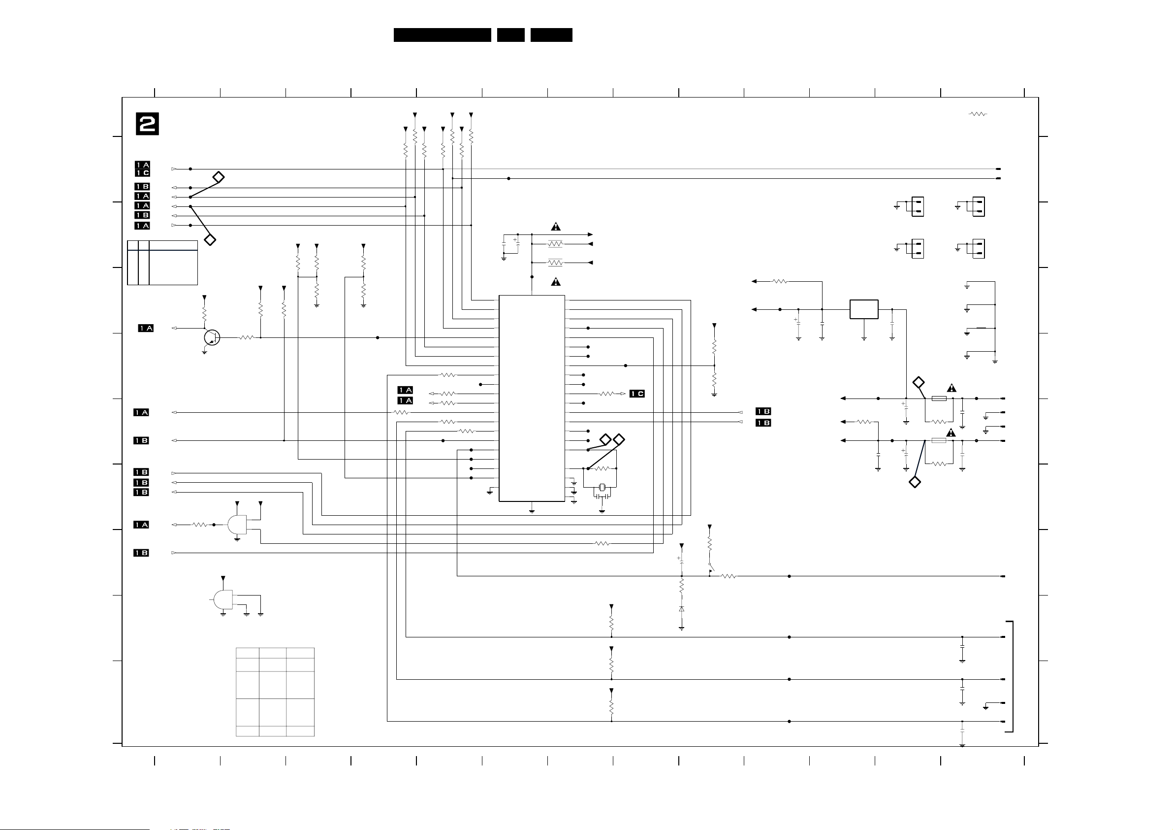
Block diagrams, Circuit diagrams and PWB’s
CD main board: Microprocessor part
GB 41CDR779 5.
A
B
S2 S1
C
D
E
F
G
H
I
PB MAIN CD-4236
CDR99
3104 123 4236
MUTE
MOT_SW
HFDET
000
n=1 disc start up
n=1 disc play
1
11
n=2 disc play
RESET
MOT_UP
TRAYSW
TRAYIN
TRAYOUT
HOMESW
+12V
10K
3311
7210
3326
3327
2305
7211
3329
3330
2308
3309
uP3V3
3115
3
VPROC
VPROC
VPROC
10K
3300
10K
10K
3305
3304
+5V
1K
1K
3310
0R
3351
+5V
3346
3352
10K
0R
F210
3353
100R
DSA_ACK
SDA
SILD
DSA_DATA
DSA_STROBE
DSA_STROBE
VPROC
VPROC
10K
3306
3318
100R
100R 3319
3354
100R
3355
100R
F217
VPROC
3302
VPROC
10K
3307
3356
100R
3303
10K
F221
F223
F224
F226
10K
F213
2300
7202
S87C654
37
P0-0|AD0
36
P0-1|AD1
35
P0-2|AD2
34
P0-3|AD3
33
P0-4|AD4
32
P0-5|AD5
31
P0-6|AD6
30
P0-7|AD7
40
P1-0
41
P1-1
42
P1-2
43
P1-3
44
P1-4
1
P1-5
2
P1-6|SCL
3
P1-7|SDA
4
RST
29
EAn|VPP
27
ALE|PROGn
26
PSENn
28
NC1
DSA_RST
F201
100n
2301
47u
F207
VCC
VSS
38
P3-0|RxD
P3-1|TxD
P3-2|INT0n
P3-3|INT1n
P3-6|WRn
P3-7|RDn
16
3308
2R2
3311
2R2
P2-0
P2-1
P2-2
P2-3
P2-4
P2-5
P2-6
P2-7
P3-4|T0
P3-5|T1
XTAL1
XTAL2
NC2
NC3
NC4
H401
1
2
VPROC
+5V
+3V3
A3V3
18
19
20
F209
21
22
F211
23
F212
24
25
F240
5
F241
7
8
F242
9
10
11
F216
12
F218
13
F222
15
F225
14
6
39
17
1M
1205
3331
100R
3328
100R3320
29 30
CST
VPROC
3335
VPROC
3337
VPROC
3339
F250
LASEROFF
12MHz
VPROC
2309
10K
10K
10K
3334
BAS216
VPROC
VPROC
3332
4u7
EVQ21
100R
6201
3357
3358
10K
1K
0R
1322
+3V3
T1
T2
3333
100R
3359
0R
F208
F228
F229
F230
F231
2302
7204
LD1117
OUT
GND
1
3360
0R
IN
F214
2306
3
2
10u
100n
2327
+5V
A12V
+12V
CONN. 1208 : TO CDR MAIN BOARD
F219
330n
2303
+12V
100n
2304
2307
H403
1
2
28
220u
100u
27
1 456789101112
2
CD MAIN BOARD - CIRCUIT DIAGRAM 2
MICROPROCESSOR PART
F200
+3V3
1K
7203
3350
1K
7005-C
74HCT08D
26
25
3312
7005-A
74HCT08D
F227
3
+5VY
14
8
7
+5VY
14
7
10
9
VPROC
TRAY
3314
10K
T1
T2
VPROC
+5V
1
2
3313
10K
uP5V
3208
3326
3327
3329
3330
3114
VPROC
3342
STBY
SCL
RW
F202
F203
S1
F204
S2
F206
BC848B
+5V
1206
MP
3344
1207
MP
3345
13
3999
1K
MUTE
1210-1
1
2
1
2
100n
100n
47p
47p
47p
H402
H404
F215
F220
1
1210-2
2
1208-16
1208-1
1208-17
1208-15
1208-7
1208-19
1208-21
1208-20
1208-18
16
1
17
15
7
19
DSA
BUS
21
20
18
ON_TRACK
HFGND
HFGND
PGND
SGND
1A
2325
0R
1A
2326
0R
2320
2321
2322
1205 F7
1206 D12
1207 E12
1208-1 E13
1208-15 E13
1208-16 D13
1208-17 E13
1208-18 I13
1208-19 H13
1208-20 I13
1208-21 I13
1208-7 G13
1210-1 A13
1210-2 A13
A
1322 G9
2300 B6
2301 B6
2302 C10
2303 C12
2304 E12
2306 E11
2307 E12
2309 G8
2320 H13
2321 I13
2322 I13
B
2325 E13
2326 E13
2327 C11
3300 A4
3302 A5
3303 A5
3304 A4
3305 A5
3306 A5
3307 A5
3308 B7
C
3309 B3
3310 B3
3311 B7
3312 C1
3313 C2
3314 D2
3318 D5
3319 D5
3320 D7
3328 F7
3331 G7
3332 G9
D
3333 G9
3334 G8
3335 H7
3337 I7
3339 I7
3342 C2
3344 E12
3345 E12
3346 B4
3350 F1
3351 C3
3352 C4
E
3353 E4
3354 E5
3355 E5
3356 E5
3357 D9
3358 D9
3359 C10
3360 E11
3999 A13
6201 H9
7005-A F1
F
7005-C G1
7202 C6
7203 D1
7204 C12
H401 A12
H402 A13
H403 B12
H404 B13
G
H
I
12
34
5
78
9101112 136
CL 96532086_018.eps
080999
Page 42
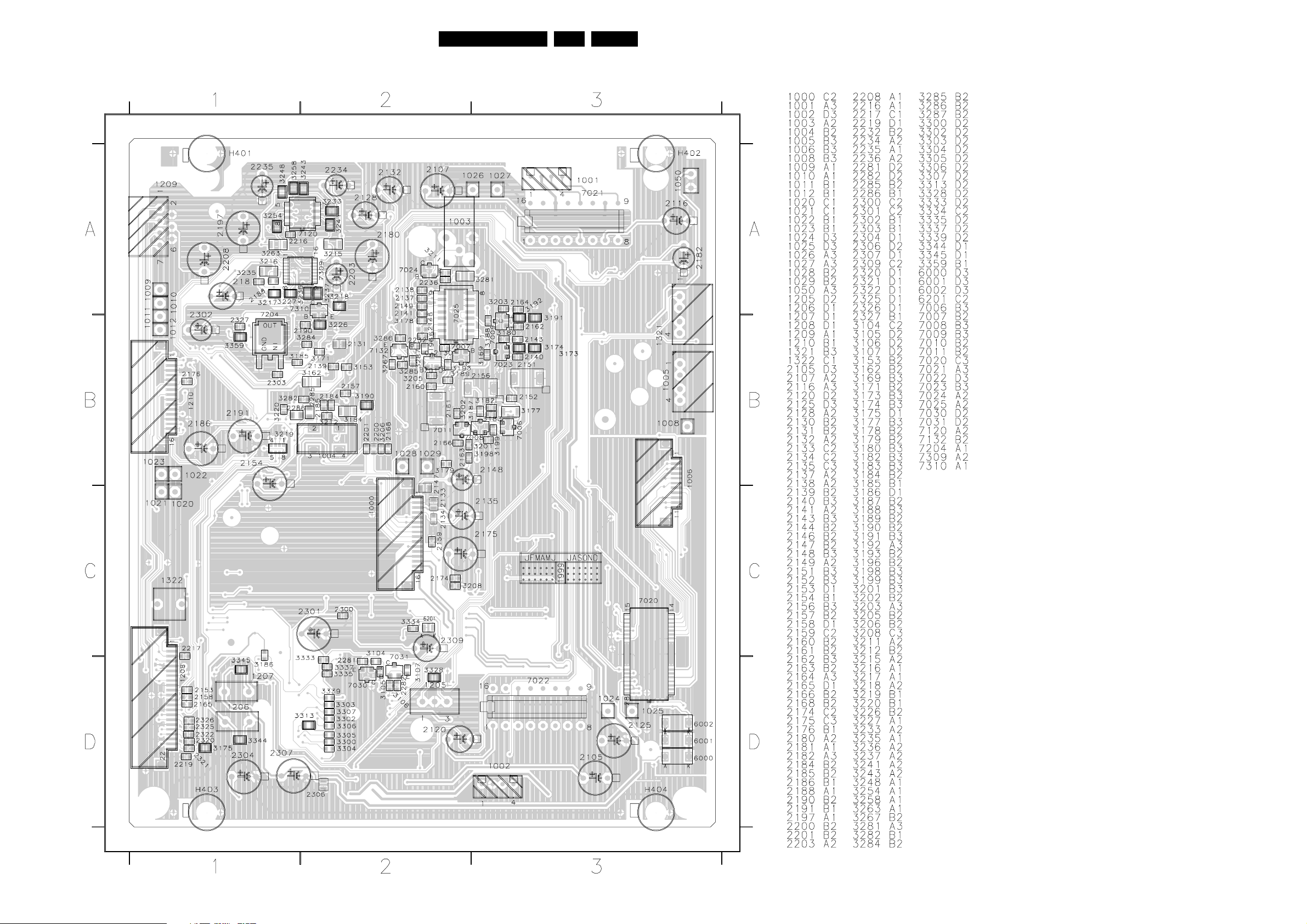
Block diagrams, Circuit diagrams and PWB’s
Layout CD Main board (top view)
CD MAIN BOARD - TOP VIEW
GB 42CDR779 5.
CL 96532086_019.eps
080999
Page 43
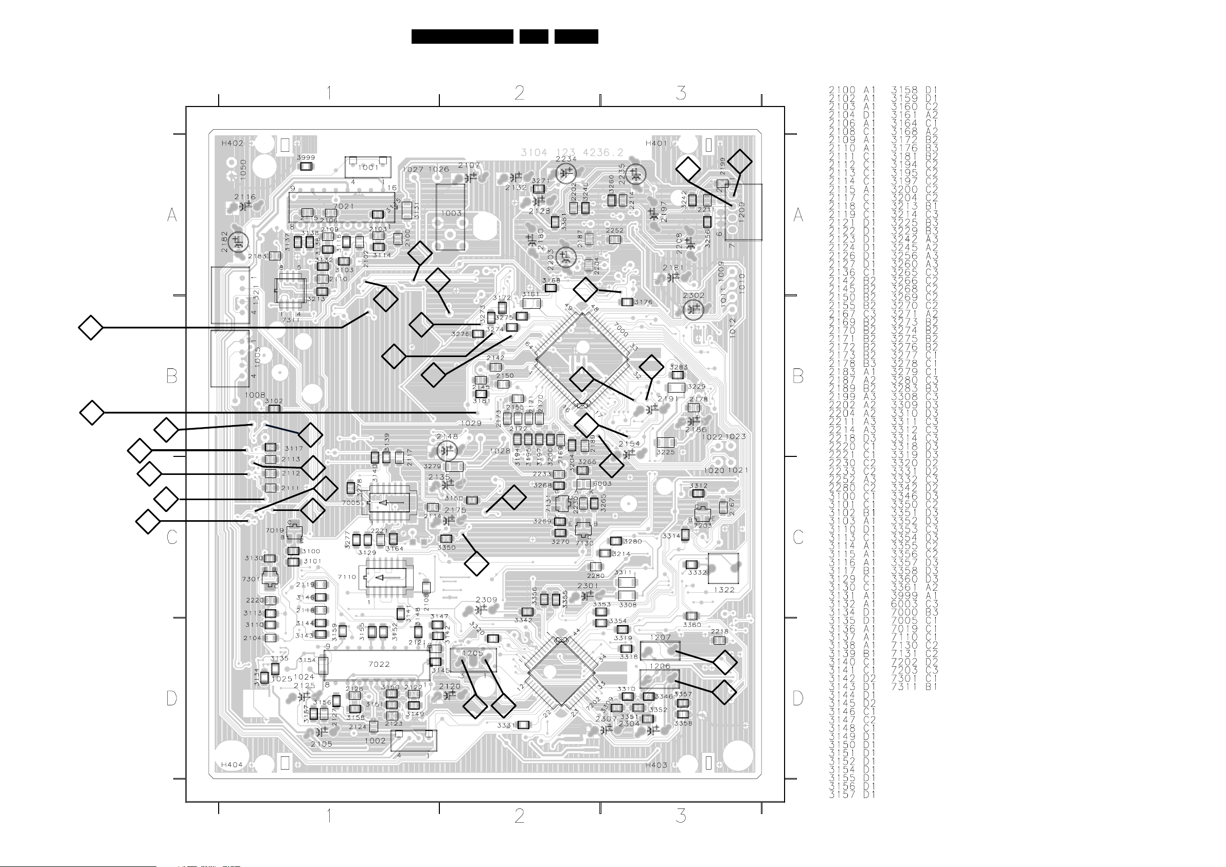
Block diagrams, Circuit diagrams and PWB’s
Layout CD Main board (bottom view)
CD MAIN BOARD - BOTTOM VIEW
GB 43CDR779 5.
24
23
26
9
10
25
2
5
4
20
6
22
3
18
19
21
13
12
14
7
17
11
1
16
15
8
30
29
27
28
CL 96532086_020.eps
080999
Page 44
Block diagrams, Circuit diagrams and PWB’s
GB 44CDR779 5.
Personal notes: Personal notes:
Page 45
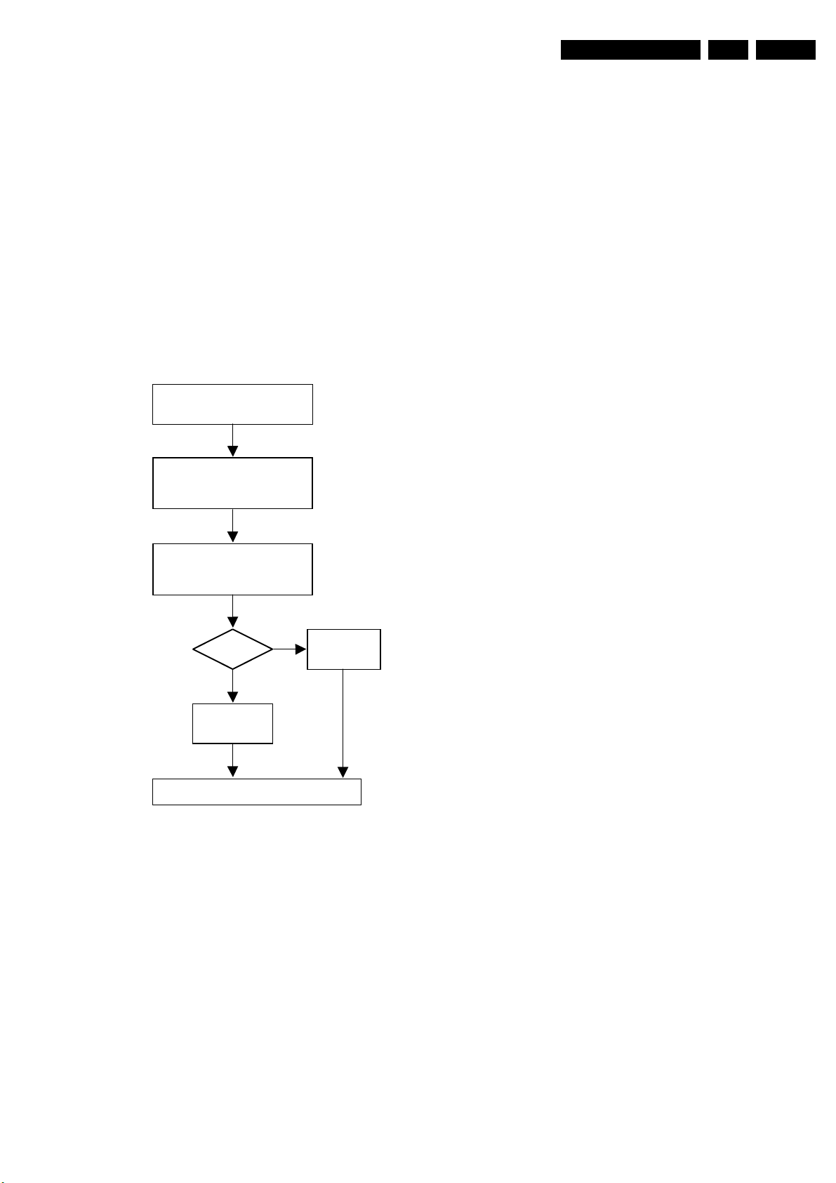
6. Diagnostic Software
6.1 Dealer mode
The purpose of the dealer mode is to prevent people taking
out the CD inside the player at exhibitions, showrooms etc..
This mode disables the open/close function of the player.
The dealer mode can be switched on and off pressing keys
[OPEN/CLOSE] and [STOP] of the CDR player
simultaneously while switching on the unit. The dealer mode
is stored in the flash memory and can only be changed by
executing the above actions.
6.2 Dealer diagnostics
DEALER DIAGNOSTICS
(status of player)
If power ON,
switch power OFF
Diagnostic Software
GB 45CDR779 6.
Press <REWIND> + <FFWD>
simultaneously and switch
ON unit
Display blinks
“BUSY”
during test
NO
Set OK?
YES
Set displays
“
PASSED
To end test, switch OFF unit
”
Figure 6-1
Set displays
“ERROR”
CL96532086-024.eps
090999
6.2.1 Description
The intention of the dealer diagnostics is to give an indication
of the CDR player status. An inexperienced, even nontechnical dealer will/can perform the test. Tests are executed
automatically without need for external tools or disassembly
of the unit. This test checks the CDR main board using the
same tests as the electrical service diagnostics program.
Only the result of the test, "PASSED" or "ERROR", will be
shown on the display. Pressing keys [F FWD] and [REWIND]
simultaneously while switching on the unit, starts the test.
Switching off the unit ends the test.
6.2.2 Requirements to perform the test
• Working keyboard to start up the test.
• Working local display to check the output messages.
Page 46
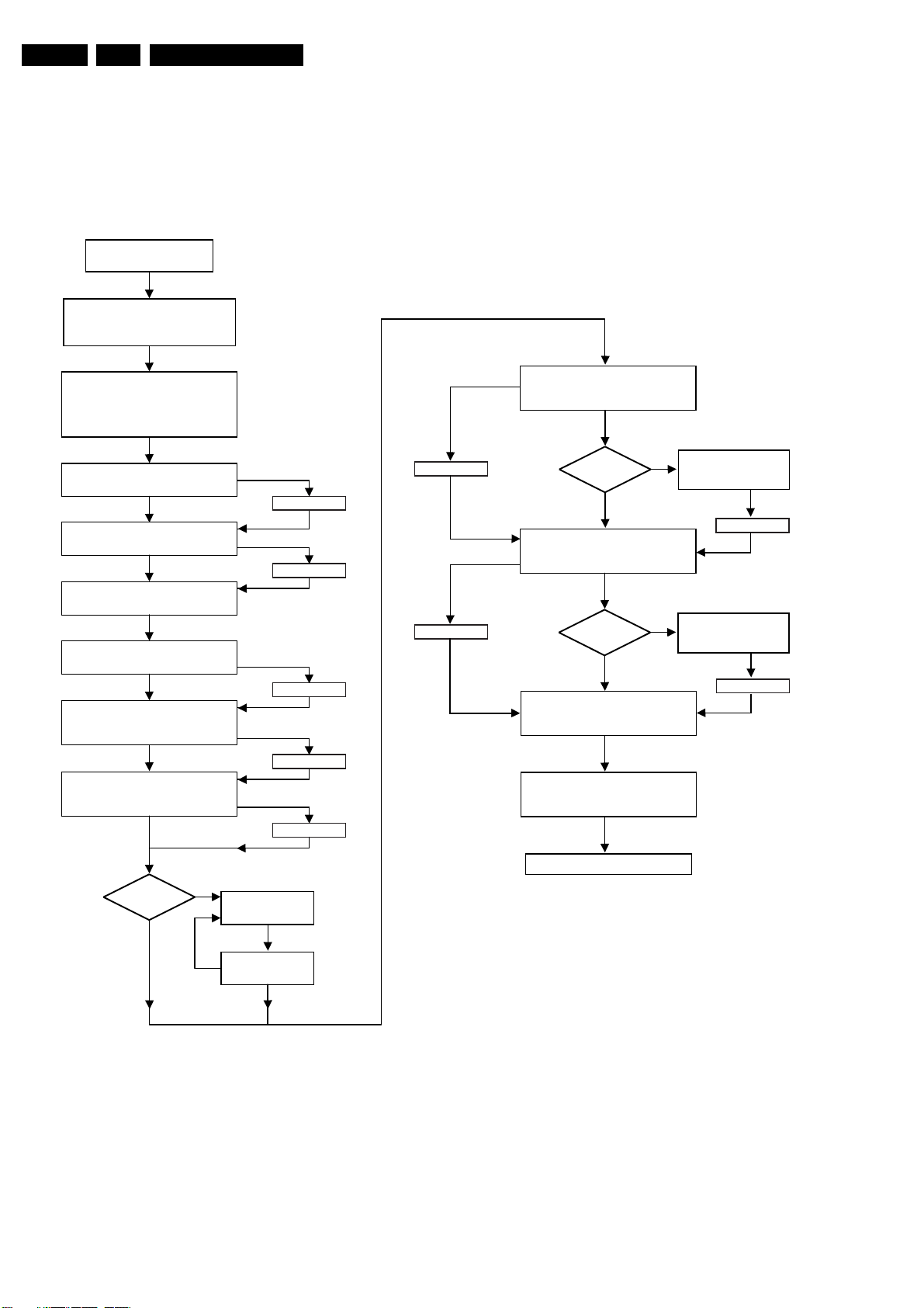
GB 46 CDR7796.
6.3 Electrical service diagnostics
ELECTRICAL SERVICE DIAGNOSTICS
(software versions, test for defective components)
If power ON,
switch power OFF
Load CD-DA disc (SBC444A)
Press <PLAY> + <F FWD>
simultaneously and switch ON unit
PLAYER
INFORMATION
Display :
"PLAYER ID"
"SW VERSION BACK END"
"SW VERSION CDR LOADER"
(CDR775
CDR MAIN
BOARD TEST
Display :
PASS OR FAIL
Display :
PASS OR FAIL
Display :
PASS OR FAIL
Display :
PASS OR FAIL
Display :
PASS OR FAIL
Display :
PASS OR FAIL
"SW VERSION CD LOADER"
"DTST1"
DRAM test (7702)
"DTST2"
FLASH CHECKSUM test (7702)
"DTST3"
FLASH ERASE test (7702)
"DTST4"
CODEC test (7702)
"DTST5"
CDR LOADER
COMMUNICATION test
"DTST6"
*
CD LOADER
COMMUNICATION test
* FOR CDR775 ONLY
)
ABORT TEST
ABORT TEST
ABORT TEST
ABORT TEST
ABORT TEST
Diagnostic Software
Press <F FWD>
Press <F FWD>
Press <F FWD>
Press <F FWD>
Press <F FWD>
ABORT TEST
Press <F FWD>
ABORT TEST
Press <F FWD>
LOADER TESTS
CDR LOADER TEST
CD-DA disc must be loaded
Display shows current disc time
Test OK?
YES
CD LOADER TEST *
CD-DA disc must be loaded
Display shows current disc time
Test OK?
YES
DISPLAY TEST
DISPLAY TEST
Display segments blink at f=1kHz
KEYBOARD &
RC TEST
KEYBOARD & RC TEST
Display shows name of pressed keys
Press <F FWD>
NO
Display :
or
or
* FOR CDR775 ONLY
NO
Display :
or
or
"BERR1"
"NO CDDA"
"NO DISC"
Press <F FWD>
"BERR2"
"NO CDDA"
"NO DISC"
Press <F FWD>
Tests OK?
YES
NO
"DERRn"
Display :
n = failed test
Display next
failed test
Figure 6-2
To end test, switch OFF unit
CL 96532086_025.eps
080999
Page 47
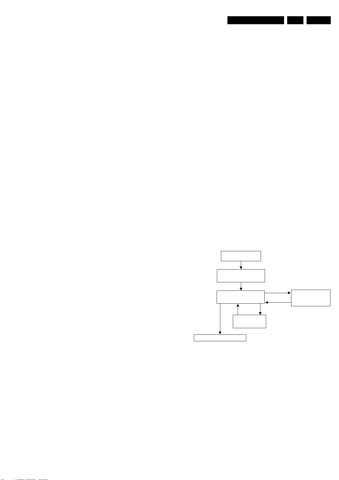
Diagnostic Software
GB 47CDR779 6.
6.3.1 Description
The intention of the electrical service diagnostics is to show
the software versions present in the player and to direct the
dealer towards defective internal units. The units are : the
CDR main board, the CDR loader, the CD loader in case of
a CDR779 and the keyboard/display board. A sequence of
tests is executed automatically. Some of the tests can be
aborted or skipped without the result being taken into
account. External tools or disassembly of the unit is not
necessary to get the diagnostic information. Pressing keys
[PLAY/PAUSE] and [F FWD] simultaneously while switching
on the unit, starts the test. Switching off the unit ends the test.
6.3.2 Requirements to perform the test
• Working keyboard to start up the test.
• Working local display to check the output messages.
• A CD-DA disc with a minimum of 3 tracks in all trays to
perform the disc test.
6.3.3 Description of the tests
Player information
In this part of the test the following important information can
be checked without removing the cover :
• Recorder ID.
• SW-version back end of player.
• SW-version CDR loader.
• SW-version CD loader (only for CDR779).
CDR main board test
[F FWD] key. The message "DERRn" will be displayed with n
indicating the faulty test number.
If one of the tests is aborted with the [F FWD] key, no error
message will be displayed for this test. The flash data erase
test ("DTST3") can not be aborted !
The CDR main board test consists out of :
DRAM test
Display : "DTST1". The DRAM used for buffer management
is tested by writing, reading and verifying test patterns.
Flash checksum test
Display : "DTST2". This test checks the checksum of the
player's SW stored in the flash.
Flash data erase
Display : "DTST3". During this test, all temporary information
(CDtxt) in the flash is erased.
is performed by audio play-back of 5 seconds at the
beginning, middle and end of the disc.
CDR loader test
During the test, the current disc time is shown. In case of an
error the message "BERR1" will be displayed and the [F
FWD] key must be pressed to continue with the following
test. Pressing the [F FWD] key also aborts this test.
CD loader test
For CDR779 only. During the test, the current disc time is
shown. In case of an error the message "BERR2" will be
displayed and the [F FWD] key must be pressed to continue
with the following test. Pressing the [F FWD] key also aborts
this test.
Display test
All segments will blink at a frequency of 1 Hz. Pressing the [F
FWD] key will start the next test because the user has to
check for himself if all segments work properly.
Keyboard and remote control tests
The test will give the user the ability to test every key without
executing the function assigned to it. Therefore, the user
needs to press every key on the keyboard and the remote
control. The display will show the name of the key being
pressed. Pressing more than one key at once will give an
unpredictable result except for the service combinations :
[PLAY/PAUSE] + [STOP], [PLAY/PAUSE] + [F FWD], [F
FWD] + [REWIND], [ERASE] + [RECORD], [PLAY/PAUSE]
+ [RECORD], [OPEN/CLOSE] + [PROGRAM].
6.4 Mechanical service diagnostics
MECHANICAL SERVICE DIAGNOSTICS
(test for defective components)
If power ON,
switch power OFF
Press <PLAY/PAUSE> + <STOP>
simultaneously and switch
ON unit
<
OPEN
<
CLOSE
>
>
Display shows
FOCUS TEST
Display shows
Visual inspection
SLEDGE TEST
Visual inspection
Display shows
“BUSY”
<FWD><REWIND>
“BUSY”
TRAY TEST
Visual inspection
“OPENED”
even if tray is blocked
CODEC (ADC/DAC) test
Display : "DTST4". This test checks the CODEC IC by
writing, reading and verifying test patterns. The test is not
applicable for CDR779.
CDR communication test
Display : "DTST5". The communication between the host
processor (DASP) and the CDR loader via the DSA-R-bus is
tested.
CD communication test
Display : "DTST6"). The communication between the host
processor (DASP) and the CD loader is tested. The test is
only applicable for CDR779.
Loader tests
These tests determine if the CDR loader and the CD loader
in case of a CDR779 work correctly. A CD-DA disc with a
minimum of 3 tracks needs to be inserted in both loaders. A
disc test is executed to check focus control, disc motor
control, radial control and jump grooves control. The disc test
To end test, switch OFF unit
Figure 6-3
6.4.1 Description
No external tools are required to perform this test. The cover
needs to be removed because the user has to check the
movements of the tray, focus and sledge visually. Pressing
keys [PLAY/PAUSE] and [STOP] simultaneously while
switching on the unit, starts the test. Switching off the unit
ends the test. In case of a CDR779, one can check the CD
loader mechanics in the same way by pressing the above key
combination on the CD player keys.
6.4.2 Requirements to perform the test
• Working keyboard to cycle through the tests and to start
up the test.
• Working local display to check the output messages.
CL96532086_026.eps
080999
Page 48
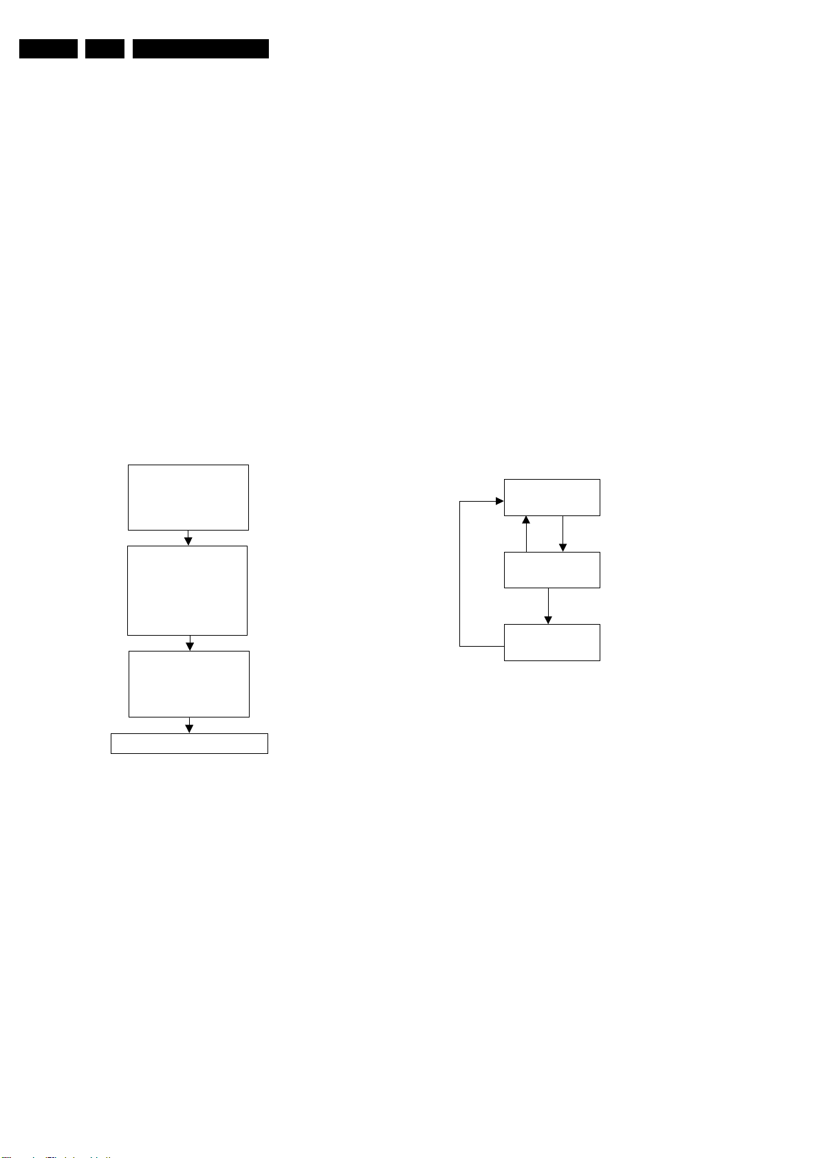
GB 48 CDR7796.
Diagnostic Software
6.4.3 Description of the tests
Focus control test
The focussing lens is continuously moving up and down. The
display reads "BUSY".
Sledge control test
After pressing [F FWD] the sledge continuously moves up
and down. Pressing [REWIND] stops the sledge at the
position it is in and the focus control test resumes. The
display reads "BUSY".
Tray control test
This test starts from within the focus control test routine.
Pressing [OPEN/CLOSE] moves the tray in or out. In the tray
open position one can initiate focus and sledge tests by
pressing [F FWD]. One has to stop these tests pressing
[REWIND] before it is possible to close the tray again.
Depending on the action the display reads "OPEN",
"OPENED", "CLOSE" or "BUSY".
6.5 DC-erase service mode
DC ERASE SERVICE MODE
(erasement of complete CD-RW)
Load CD-RW disc
Press
<ERASE> + <RECORD>
simultaneously and switch
ON unit
Display shows:
ER mm:ss
“
mm
ss :remaining seconds
TOTAL
and
illuminated
Display shows:
“
when the erase function is
if DC ERASE fails
To end test, switch OFF unit
Figure 6-4
6.5.1 Description
This test is initiated by pressing [ERASE] and [RECORD]
simultaneously while switching on the unit. The player will
erase a complete CD-RW disc (including PMA and ATIP lead
out area) at speed N=2. The display shows the countdown of
the remaining time required for the operation to complete.
The format is "ER mm:ss", where "mm" are the remaining
minutes and "ss" the remaining seconds. After completion
the message "PASSED" is shown, and the player has to be
switched off and on again to start up in normal operating
mode. Switching off the unit before completion of the test,
leaves the disc in an unpredictable state. In such case only a
complete DC-erase procedure can recover the CD-RW disc.
6.5.2 Requirements to perform the test
• Functional CDR player.
• A CD-RW audio disc must be present in the tray.
”
:remaining minutes
REM
are also
PASSED
”
completed
ERROR
”
“
CL96532086_027.eps
080999
6.6 Burn in mode
6.6.1 Description:
The Burn In mode is an endless cycle of:
• DC-Erase to erase the CDRW disc with maximum laser
power.
• Recording a CDRW disc
• Finalising at double speed
The Burn In mode is used to test intermittent faults of the
loader.
6.6.2 Requirements to perform the test:
• Working Local Keyboard: needed to start up the test.
• Working Local Display: all output messages must be
displayed on the local display.
• Analog source connected to the CDR99 player
• CDRW disc in tray
Burn in sequence
– Initialisation
The ‘Burn In’ mode is initiated by pressing the [PLAY/
PAUSE] and [RECORD] key on the local keyboard at the
same time, and then switching the POWER switch on.
– Continuous loop
The following picture shows the burn in sequence.
DC erase
error
Finalise
complete with
or without
error
Write CDRW
Finalise
Figure 6-5 Burn in sequence
Continuously do DC erase, record complete CDRW and then
finalise until the player is powered off.
When an error is detected during writing, the DC erase
procedure is called again., the disc will be DC erased and the
cycle starts again.
During the test the display shows the number of hours for
which the test is running and the number of errors detected
during the test. The display looks as follows : “HH BI RE FE”
HH : number of hours on
“BI” : burn in mode, digits
RE : number of errors
FE : number of errors
If started up with a disc other than
a CDRW disc the display shows : ”WRONG DISC”,
if no disc is inserted display : “NO DISC”.
– End of test
To exit the Burn In mode, power off the player.
Erase complete without error
Write complete without error
digits 1 and 2
3 and 4
detected during DC
erase and write
CDRW modes on
digits 7 and 8
detected during
finalise modes on
digits 10 and 11
CL06532018_101.eps
301100
Page 49
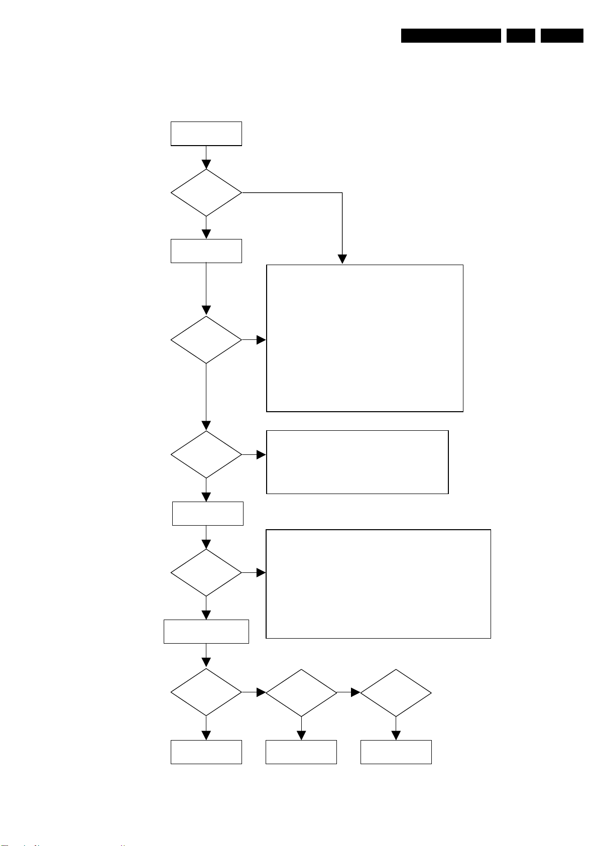
7. Faultfinding trees
7.1 CDR-Module
NO DISC LOADED
SWITCH ON POWER
Faultfinding trees
GB 49CDR779 7.
STBY LED?
YES
PRESS <DISPLAY>
DISPLAY?
YES
DISPLAY:
"INSERT DISC"
YES
NO
CHECK:
• MAINS, MAINS CABLE
• POWER SUPPLY (SEE FAULT FINDING GUIDE PSU)
⇒
WIRING
⇒
ON/OFF SWITCH
⇒
FUSES
⇒
NO
• DISPLAY (SEE FAULT FINDING GUIDE DISPLAY BOARD)
CHECK:
NO
• WIRING
• POWER SUPPLY VOLTAGES
• ELECTRICAL SERVICE DIAGNOSTICS:
REPLACE CDR MODULE IF
OR
VOLTAGES
⇒
WIRING
⇒
SUPPLY VOLTAGES
⇒
CLOCK SIGNAL 8MHz
⇒
CONTROL SIGNALS
⇒
KEYBOARD
⇒
STANDBY LED
⇒
ELECTRICAL SERVICE DIAGNOSTICS:
DISPLAY TEST, KEYBOARD TEST
"BERRn"
ERROR OCCURS
"DERRn"
PRESS
<OPEN/CLOSE>
TRAY?
YES
INSERT DISC
PRESS <OPEN/CLOSE>
CD-DA DISC
LOADED?
SEE CD-DA DISC
FAULT FINDING
CHECK:
• DISPLAY BOARD (SEE FAULT FINDING GUIDE DISPLAY BOARD)
⇒
NO
• MECHANICAL SERVICE DIAGNOSTICS:
REPLACE CDR MODULE IF ERROR OCCURS
SEE CD-R DISC
FAULT FINDING
WIRING
⇒
SUPPLY VOLTAGES
⇒
CLOCK SIGNAL 8MHz
⇒
CONTROL SIGNALS
⇒
KEYBOARD
⇒
ELECTRICAL SERVICE DIAGNOSTICS:
DISPLAY TEST, KEYBOARD TEST
CD-R DISC
LOADED?
YESYES
NONO
CD-RW DISC
LOADED?
YES
SEE CD-RW DISC
FAULT FINDING
Figure 7-1
CL 96532076_016.eps
290799
Page 50
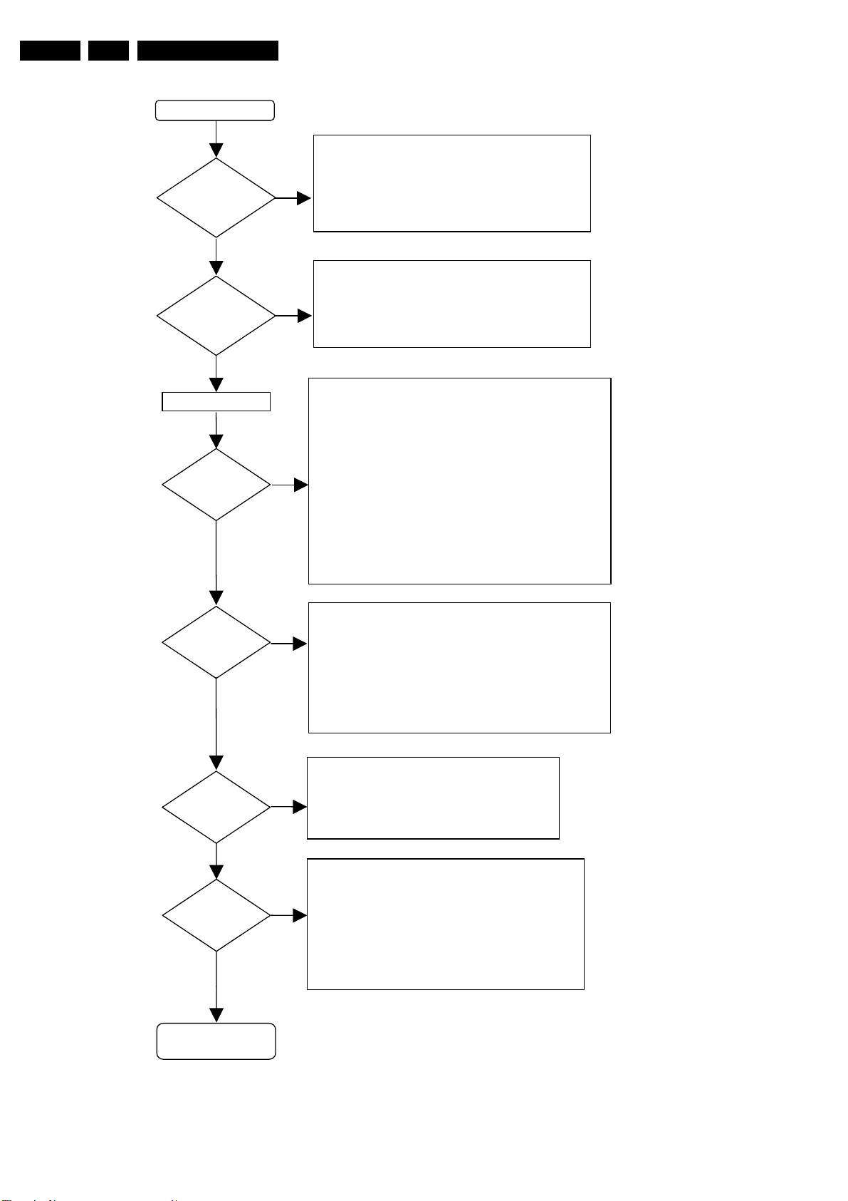
GB 50 CDR7797.
CD-DA DISC LOADED
DISC
DETECTION &
READING?
YES
DISPLAY:
“CD”
&
T.O.C. INFO?
YES
Faultfinding trees
CHECK:
• WIRING
• POWER SUPPLY VOLTAGES
NO
• ELECTRICAL SERVICE DIAGNOSTICS:
REPLACE CDR MODULE IF
OR
"BERRn"
CHECK:
• DISC: DIRT, SCRATCHES, DAMAGED...
NO
• ELECTRICAL SERVICE DIAGNOSTICS:
REPLACE CDR MODULE IF
OR
"BERRn"
ERROR OCCURS
ERROR OCCURS
"DERRn"
"DERRn"
PRESS <PLAY>
ANALOG
AUDIO
OUT?
YES
DISTORTION?
NO
HEADPHONE?
YES
DIGITAL
AUDIO
OUT?
YES
CHECK:
AUDIO CONNECTIONS & CABLES
•
I/O BOARD
•
⇒
FLEX CONNECTION
⇒
+5V (pin 8 conn. 1000)
⇒
NO
• ELECTRICAL SERVICE DIAGNOSTICS:
REPLACE CDR MODULE IF
OR
CHECK:
YES
NO
NO
AUDIO CONNECTIONS & CABLES
•
I/O BOARD
•
• ELECTRICAL SERVICE DIAGNOSTICS:
REPLACE CDR MODULE IF
OR
CHECK:
WIRING OF HEADPHONE/IR BOARD
•
• ELECTRICAL SERVICE DIAGNOSTICS:
REPLACE CDR MODULE IF
OR
CHECK:
AUDIO CONNECTIONS & CABLES
•
I/O BOARD
•
• ELECTRICAL SERVICE DIAGNOSTICS:
REPLACE CDR MODULE IF
OR
KILL VOLTAGE (pin 7 conn. 1000):
-8V DURING PLAY
⇒
KILL TRANSISTORS 7006,7007,7008, 7009
PLAY AUDIO SIGNALS DISC TRACK 15:
⇒
SIGNAL OF 5.4 VPP ON PINS 1 AND 3 OF CONN.
1000
"BERRn"
"BERRn"
"BERRn"
⇒
⇒
⇒
"BERRn"
ERROR OCCURS
⇒
FLEX CONNECTION
⇒
+5V (pin 8 conn. 1000)
ERROR OCCURS
ERROR OCCURS
FLEX CONNECTION
+5V (pin 8 conn. 1000)
DIGITAL OUT TRANSFORMER 5450, IC7005
ERROR OCCURS
"DERRn"
"DERRn"
"DERRn"
"DERRn"
PLAY BACK OF CD-DA
DISCS OK
Figure 7-2
CL 96532076_017.eps
290799
Page 51
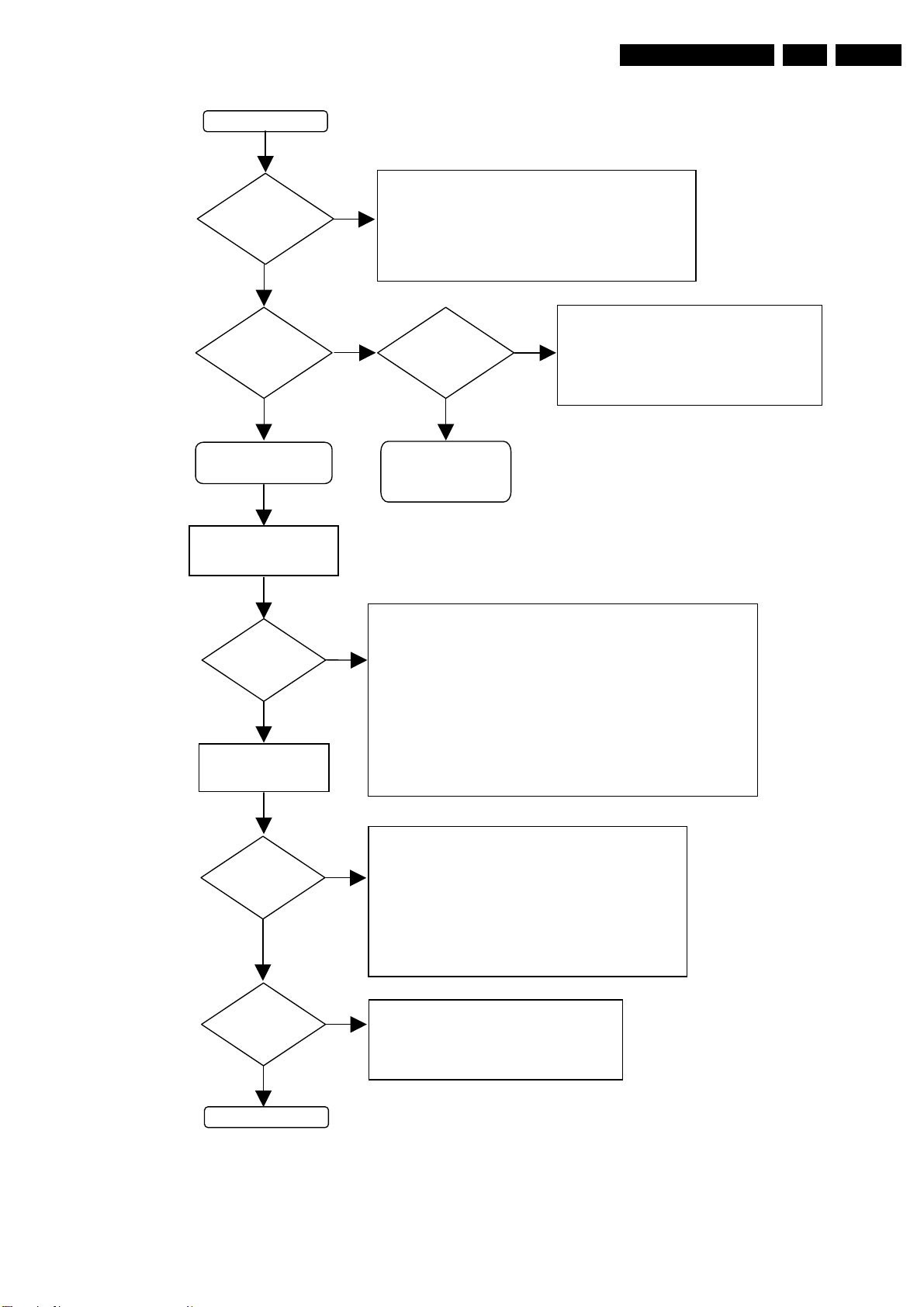
CD-R DISC LOADED
DISC
DETECTION &
READING?
YES
DISPLAY:
“CD R”
OPC INFO?
&
YES
Faultfinding trees
CHECK:
NO
• WIRING
• POWER SUPPLY VOLTAGES
• ELECTRICAL SERVICE DIAGNOSTICS:
REPLACE CDR MODULE IF
OR
NO
"BERRn"
DISPLAY:
T.O.C. INFO?
YES
“CD”
&
ERROR OCCURS
"DERRn"
CHECK:
NO
• DISC: DIRT, SCRATCHES, DAMAGED...
• ELECTRICAL SERVICE DIAGNOSTICS:
REPLACE CDR MODULE IF
OR
"BERRn"
ERROR OCCURS
GB 51CDR779 7.
"DERRn"
CD-R DISC PARTIALLY
RECORDED OR EMPTY
START MANUAL
RECORDING FROM
ANALOG SOURCE
LEVEL
ADJUSTABLE?
YES
START RECORDING
FROM DIGITAL
SOURCE
DIGITAL IN?
OPTICAL IN?
YES
FINALISED CD-R DISC
LOADED
SEE CD-DA DISC
FAULT FINDING
CHECK:
AUDIO CONNECTIONS & CABLES
•
NO
• DISPLAY BOARD (SEE FAULT FINDING GUIDE DISPLAY BOARD)
•
• ELECTRICAL SERVICE DIAGNOSTICS:
CHECK:
•
NO
•
• ELECTRICAL SERVICE DIAGNOSTICS:
⇒
EASY JOG KNOB
⇒
I2C COMMUNICATION
⇒
ELECTRICAL SERVICE DIAGNOSTICS:
KEYBOARD TEST
REPLACE CDR MODULE IF
OR
"BERRn"
AUDIO CONNECTIONS & CABLES
I/O BOARD
⇒
⇒
⇒
REPLACE CDR MODULE IF
OR
"BERRn"
ERROR OCCURS
FLEX CONNECTION
+5V (pin 8 conn. 1000)
IC7005, OPTICAL RECEIVER 6000
ERROR OCCURS
"DERRn"
"DERRn"
RECORDING
SUCCESSFUL?
YES
SET OK
NO
CHECK:
• ELECTRICAL SERVICE DIAGNOSTICS:
REPLACE CDR MODULE IF
OR
"BERRn"
ERROR OCCURS
Figure 7-3
"DERRn"
CL 96532076_018.eps
290799
Page 52
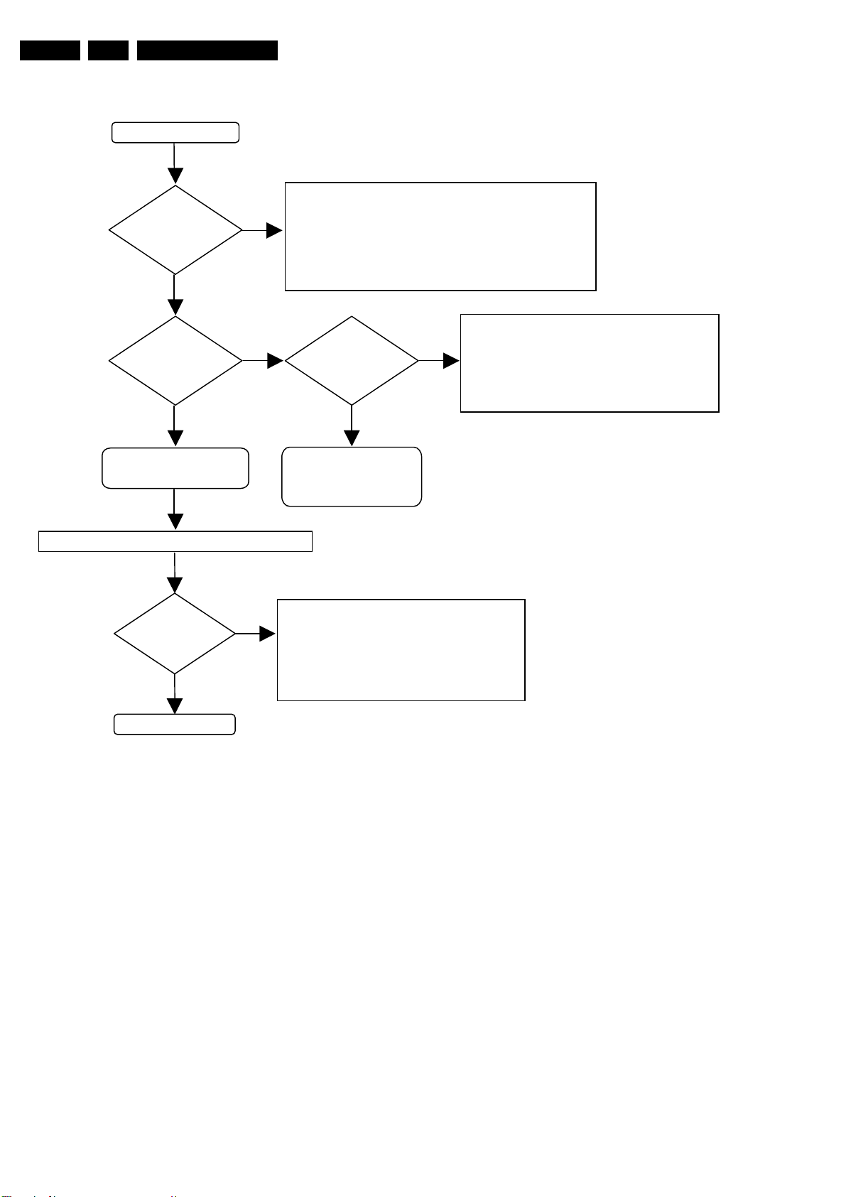
GB 52 CDR7797.
CD-RW DISC LOADED
DISC
DETECTION &
READING?
YES
DISPLAY:
“CD RW”
OPC INFO?
YES
&
NO
NO
Faultfinding trees
CHECK:
• WIRING
• POWER SUPPLY VOLTAGES
• ELECTRICAL SERVICE DIAGNOSTICS:
REPLACE CDR MODULE IF
OR
"BERRn"
DISPLAY:
“CD”
T.O.C. INFO?
YES
ERROR OCCURS
&
NO
"DERRn"
CHECK:
• DISC: DIRT, SCRATCHES, DAMAGED...
• ELECTRICAL SERVICE DIAGNOSTICS:
REPLACE CDR MODULE IF
OR
"BERRn"
ERROR OCCURS
"DERRn"
CD-RW DISC PARTIALLY
RECORDED OR EMPTY
START ERASING OF LAST RECORDED TRACK
ERASING
SUCCESSFUL?
YES
SET OK
NO
FINALISED CD-RW DISC
CHECK:
• ELECTRICAL SERVICE DIAGNOSTICS:
•
LOADED
SEE CD-DA DISC
FAULT FINDING
REPLACE CDR MODULE IF
OR
"BERRn"
IF DISC CORRUPTED TRY DC ERASE
ERROR OCCURS
Figure 7-4
"DERRn"
CL 96532076_019.eps
290799
Page 53
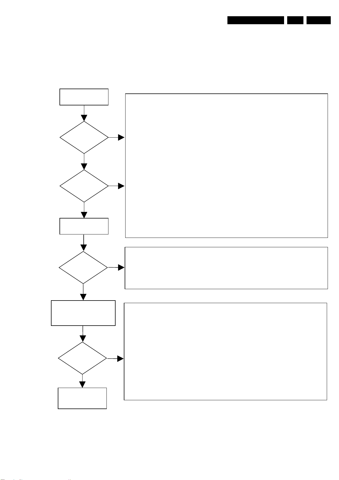
7.2 CD Module
CD MODULE
NO DISC
POWER ON
DISC
DETECTION
STARTS?
YES
DISPLAY?
YES
PRESS
<OPEN/CLOSE>
NO
NO
Faultfinding trees
• CHECK FLEX CONNECTION FROM CDR MAIN BOARD
• POWER SUPPLY
⇒ +5V, +12V AT TESTPOINTS 28 AND 27
⇒ +5V AT CONN. 1000 PINS 1 AND 3
⇒ +5V AT IC7005 PIN 14
⇒ +3V3 AT IC7000 PINS 5,17,21,57, CHECK SAFETY RESISTORS
⇒ +5V AT IC7020 PIN 25
⇒ +10V AT IC7020 PINS 26, 27, 28
⇒ +12V AT IC7021 PIN 5, CHECK SAFETY RESISTOR R3131
⇒ +12V AT IC7022 PIN 5, CHECK SAFETY RESISTOR R3154
⇒ +5V AT IC7025 PIN 16
⇒ +5V AT IC7202 PIN 38, CHECK SAFETY RESISTOR R3308
⇒ +3V3 AT IC7309 PINS 4 AND 13, CHECK SAFETY RESISTORS R3215, R3216
⇒ +12V AT IC7120 PIN 8, CHECK SAFETY RESISTOR R3263
• CLOCKS
⇒ 8.4672MHz AT TESTPOINT 7
⇒ 12MHz AT TESTPOINTS 29 AND 30
⇒ 11.2896 AT TESTPOINT 10
⇒ 2.1168MHz AT TESPOINT 20
⇒ 44.1kHz AT TESTPOINT 21
• DISPLAY
⇒ SEE FAULTFINDING GUIDE DISPLAY BOARD
• MICROPROCESSOR 7202
GB 53CDR779 7.
TRAY?
YES
LOAD DISC
(CD-DA OR PARTIALLY
RECORDED CD-R/CD-RW)
PRESS <OPEN/CLOSE>
NO
TOC?
YES
SEE NEXT PAGE:
PLAYBACK
DIAGNOSTIC SOFTWARE : MECHANICAL SERVICE DIAGNOSTICS CD LOADER : TRAY TEST
NO
•
• HF PATH
• REPLACE OR REPAIR CD LOADER ASSY (CDM MECHANISM)
⇒ CHECK TRAY MOTOR VOLTAGES
⇒ MICROPROCESSOR 7202
⇒ CHECK TRAY MOTOR DRIVER IC7021
⇒ REPLACE OR REPAIR CD LOADER ASSY:
TRAY MOTOR ASSY 02, BELT 11
DIAGNOSTIC SOFTWARE : MECHANICAL SERVICE DIAGNOSTICS CD LOADER :
⇒ CHECK WIRING TO CDM
⇒ CHECK POWER DRIVERS 7021, 7022, 7020
⇒ CHECK VOLTAGES ON POWER DRIVERS (SEE CIRCUIT DIAGRAMS)
⇒ TESTPOINTS 4, 5, 6 : PULSE DENSITY MODULATED SIGNALS
⇒ TESTPOINTS 1, 2, 3, 9 : EYEPATTERN
⇒
CHECK
CDRW DISC. EYEPATTERN OF CDRW DISC WILL BE AMPLIFIED (≈ X 2.5).
EYEPATTERN OF CDDA DISC WILL BE ATTENUATED(
⇒
CHECK
⇒ TESTPOINTS 20, 21, 22: I2S
RW
S1,S2
FOCUS TEST & SLEDGE TEST
AT TESTPOINT 8 : HIGH FOR CDDA AND CDR DISC, LOW FOR
AT TESTPOINTS 25 AND 26 (SEE CIRCUIT DIAGRAMS)
DATA, WCLK, SCLK
TRAY+, TRAY-
≈ X 0.8)
CL 96532086_030.eps
080999
Figure 7-5
Page 54
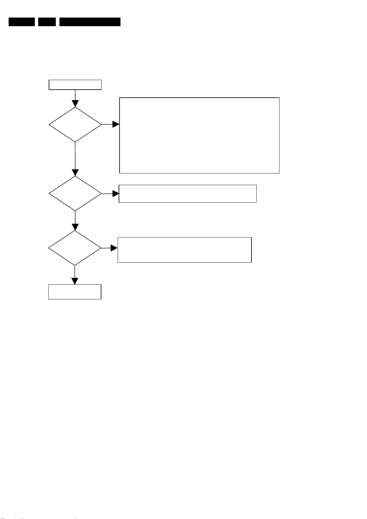
GB 54 CDR7797.
Faultfinding trees
CD MODULE PLAYBACK
PRESS <PLAY>
• DAC 7309
⇒ TESTPOINTS 20, 21, 22 : I2S AT INPUT OF DAC 7309
⇒ CHECK POWER SUPPLY PINS 4, 13
⇒ CHECK CLK11 AT PIN 6 : 11.2896MHz
⇒ PIN 11 : MUTE HIGH?
⇒ TESTPOINTS 23, 24 : ANALOG OUTPUT?
⇒ REPLACE DAC 7309
• OPAMP 7120
AUDIO?
YES
NO
⇒ TESTPOINTS 23, 24 : ANALOG OUTPUT?
⇒ POWER SUPPLY: PIN 8→12V
⇒ REPLACE OPAMP 7120
DISTORTION?
NO
AUDIO
CD OUT PCB?
YES
PLAYBACK CD
MODULE OK
YES
NO
• DAC 7309
• OPAMP 7120
• FLEX TO CDR MAINBOARD
• FLEX TO CD OUT BOARD
• CHECK I/O BOARD, CD OUT BOARD
Figure 7-6
CL 96532086_031.eps
080999
Page 55
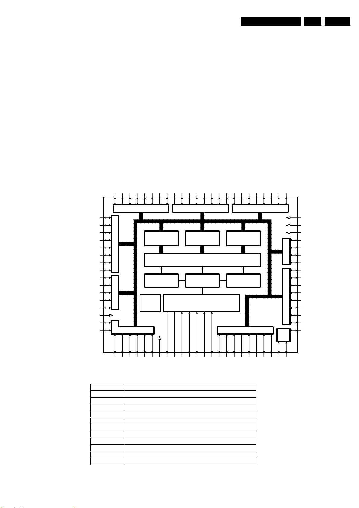
8. Faultfinding Guide
Faultfinding Guide
GB 55CDR779 8.
8.1 Display Board
8.1.1 Description of display board
General description
The display board has three major parts : the FTD
(Fluorescent Tube Display), the display controller
TMP87C874F and the keyboard. The display controller is
controlled by the DASP master processor on the CDR main
board. The communication protocol used is I2C. So all the
information between DASP and display controller goes via
the SDA or I2C DATA and SCL or I2C CLK lines.
Communication is always initiated by the DASP on the CDR
main board. Unlike the previous generations of CDR players,
the interrupt generated by the display controller at key-press
or reception of remote control is not used. Instead, the DASP
polls the display controller for these events.
BLOCK DIAGRAM
TMP87C874F
64 63 62 61 60 59 58 57 56 55254 53
I/O PORT8 (VFT)
65
66
67
68
69
70
71
72
73
74
75
76
77
78
79
80
I/O PORTD (VFT) I/O PORT9 (VFT)
VKK
I/O PORT0
3
1
DATA MEMORY
TIMER/COUNTER
8 BIT A/D
CONVERT.
I/O PORT7 (VFT)
( RAM )
512X8 BIT
16 BIT
CLOCK/TIMING CONTROLLER
VSS1
RESETN
XOUT
XIN
79819
10
52
PROGR MEMORY
( ROM )
8kX8 BIT
C P U
INTERRUPT
CONTROLLER
( I/O PORT2 )
P22
P21
TEST1
P20
13
141211 17 18 20 21 22
Display controller TMP87C874F
TMP87C874F (IC7104) is a high speed and high
performance 8-bit single chip microprocessor, containing 8bit A/D conversion inputs and a VFT (Vacuum Fluorescent
Tube) driver. In this application, its functions are :
• slave microprocessor.
• FTD driver.
• generates the square wave for the filament voltage
required for an AC FTD.
• generates the grid and segment scanning for the FTD.
• generates the scanning grid for the key matrix.
• input for remote control.
All the communication runs via the serial bus interface I2C.
The display controller uses an 8MHz resonator as clock
driver.
41
42434445464748495051
I/O PORT6 (VFT)
I/O PORT5
I/O PORT4
2
SDA
40
39
38
37
36
35
34
33
32
31
30
29
28
27
26
25
SCK0
PROGRAM
COUNTER
TIMER/COUNTER
INT0
INT1
8 BIT
I/O PORT1
VDD
VAREF
VASS
I C
PORT3
SCL
23 244
PIN DESCRIPTIONS
INT0 external interrupt input 0
INT1 external interrupt input 1
RESETN reset signal input, active low
SCL I2C-bus serial clock input/output
SDA I2C-bus serial data input/output
TEST test pin, tied to low
VAREF analog reference voltage input
VASS analog reference ground
VDD +5V
VKK VFT driver power supply
VSS ground
XIN, XOUT resonator connecting pins for high-frequency clock
Figure 8-1
CL 96532076_028.eps
290799
Page 56
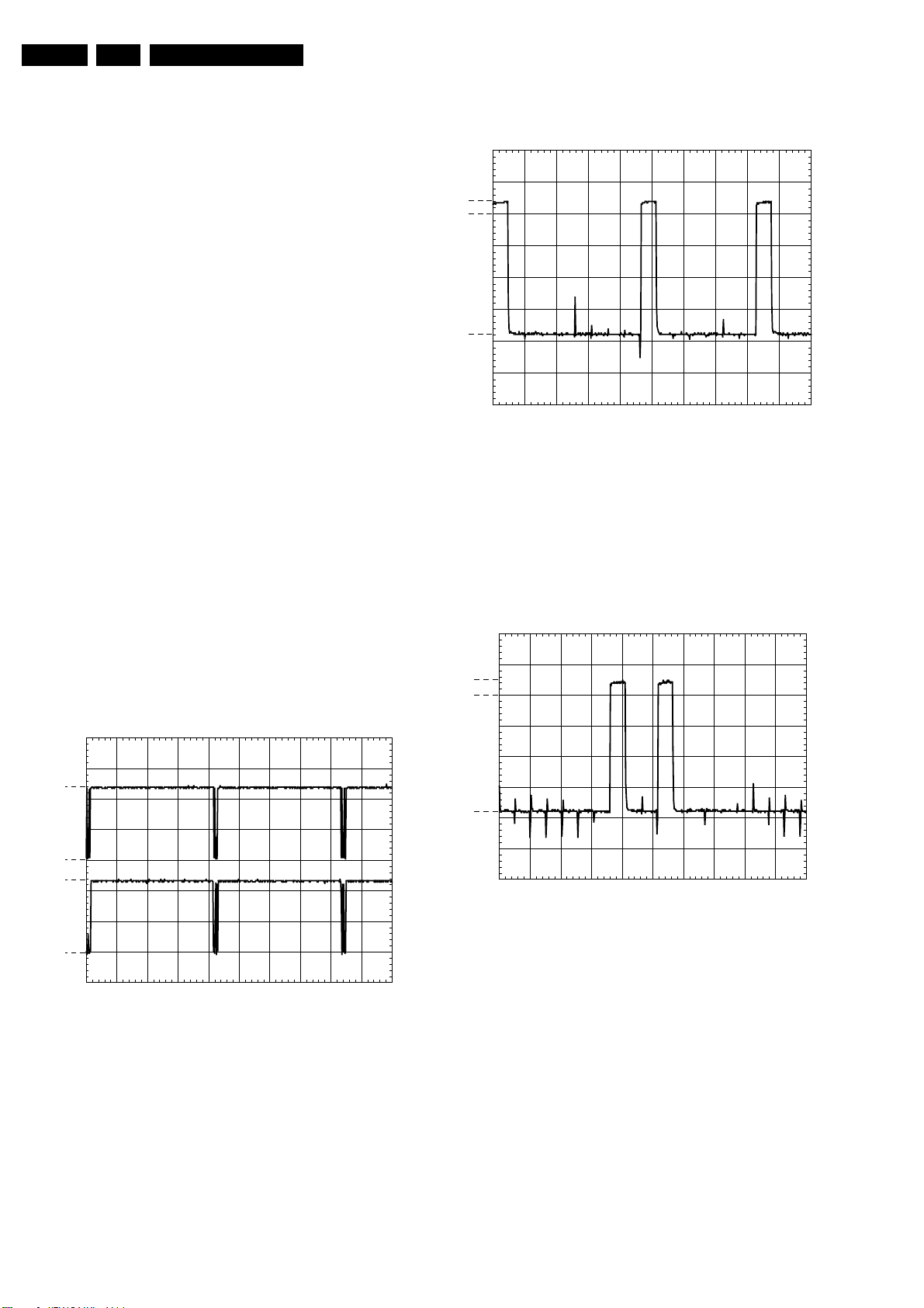
GB 56 CDR7798.
Faultfinding Guide
8.1.2 Test instructions
Supply voltages
The display board receives several voltages via connector
1119 (and connector 1121 for CDR570/930).
• VFTD : -38V ±5% measured at pin 2 of conn. 1119.
• VDC1-VDC2 : 3V8 ±10% measured between pin 1 and 3
of conn. 1119.
• +5V : +5V ±5% measured at pin 10 of conn. 1119 (pin 4
of conn. 1121 for CDR770).
Voltages VFTD, VDC1 and VDC2 are produced in the power
supply unit and sent to the display board via the CDR main
board. The +5V voltage is produced on the CDR main board
as D5V.
Clock signal
As clock driver for the display controller, a resonator of 8 MHz
(1110) is used. The signal can be measured at pins 8 and 9
of the display controller : 8 MHz ±5%.
Control signals
RESET
The reset signal comes via pin 4 of conn. 1119 from the
DASP master processor on the CDR main board
(SYS_RESET). The reset is low active. It should be kept low
during power up for at least 3 machine cycles with supply
voltage in operating range and a stable clock signal (1
machine cycle = 12 x 1/Fc (8 MHz) sec.). During normal
operation, the reset should be high (3V3). The high signal is
3V3 because the DASP operates on 3V3.
I2C DATA/I2C CLK
These lines connect to the DASP master processor via
respectively pin 5 and pin 7 of conn. 1119 (pin 5 of conn.
1119 and pin 1 of conn. 1121 for CDR570/930). When there
is no communication, they should have the high level (+5V).
The oscillogram below gives an indication of how these
signals should look like.
line : T7203 for G13, T7204 for G14 and T7100 for G15. A
typical grid line signal shows in the oscillogram below.
PM3392A
+4V
0V
-38V
CH1!10.0 V= MTB1.00ms ch1+
Figure 8-3 ‘Gridline’
Segment lines
Level and timing of all segment lines, P1-->P21 (P1-->P20
for CDR770), can be checked either at the FTD itself or at the
display controller. The data on these segment lines however,
depends on the characters displayed. The oscillogram below
shows a segment line with data. A segment line without data
maintains a -38V level.
PM3392A
+5V
0V
CL 96532076_024.eps
301100
PM3392A
+5V
I2C DATA
0V
+5V
I2C CLK
0V
CH1!2.00 V=
CH2 2 V= MTB10.0ms ch1+
CL 96532076_025.eps
Figure 8-2 ‘I2C signals’
FTD drive lines
Filament voltage
Should measure 3.8V ±10% (=VDC1-VDC2) between pins 12-3 and pins 45-46-47 (pins 1-2 and pins 48-49 for CDR770)
of the FTD (1113).
301100
-38V
CH1!10.0 V= MTB1.00ms ch1+
CL 96532076_027.eps
Figure 8-4 ‘Segment line’
Key matrix lines
The lines connected to pins 34, 35, 36 and 37 of the display
controller act as matrix scanners. Without a key pressed,
they maintain a low level. As soon as a key is pressed, the
scanning line connected to that key puts out a scanning
signal, which should look like the oscillogram below. This
scanning signal goes via the pressed key to I/O port 4 of the
display controller (pins 28 to 33). The display controller can
now determine which key has been pressed. Without a key
pressed, pins 28 to 33 of the display controller maintain a
high level (+5V).
301100
Grid lines
Level and timing of all grid lines, G1-->G15, can be checked
either at the FTD itself or at the display controller. Grid lines
G13, G14 and G15 each have an extra current amplifier in
Page 57
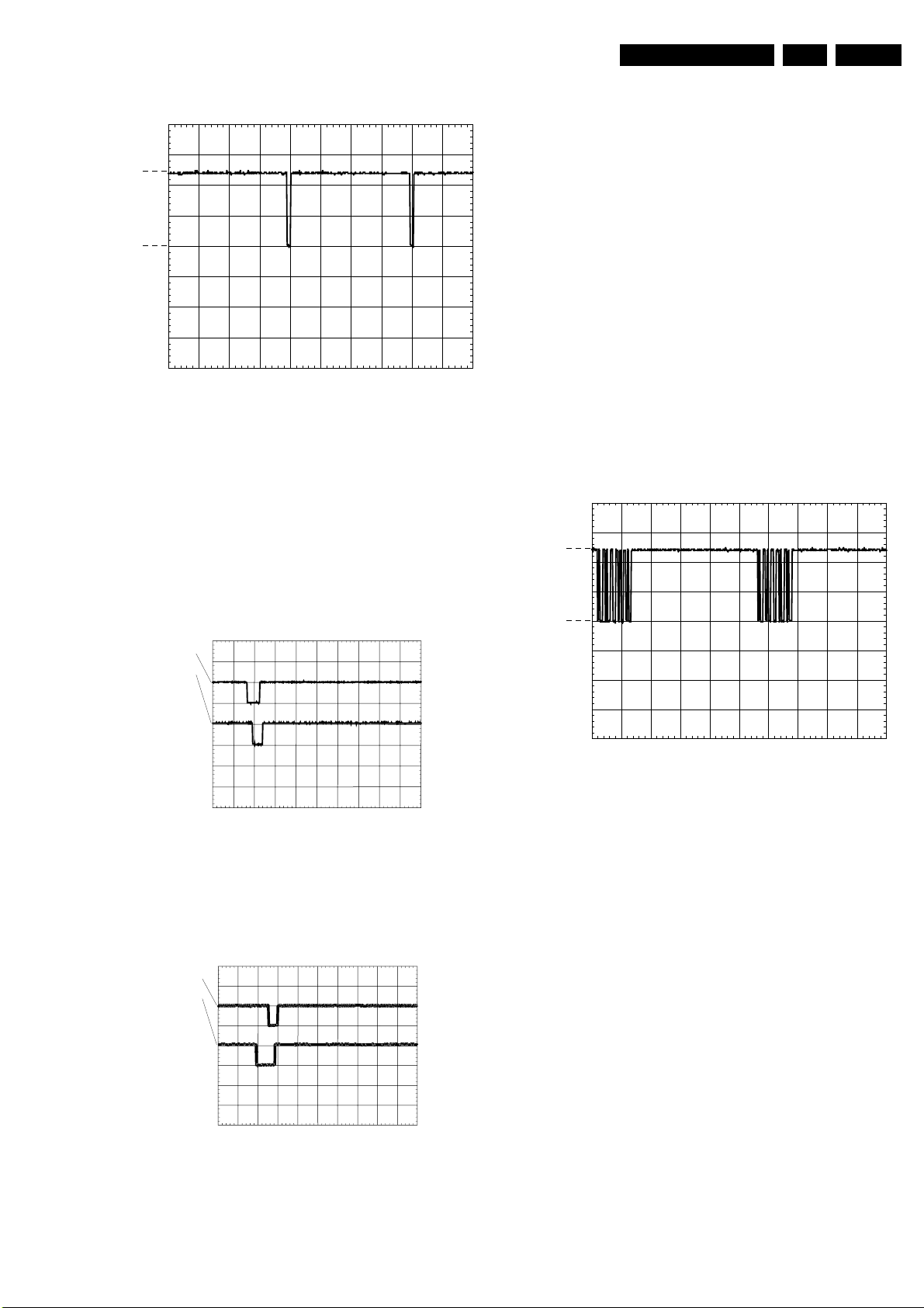
PM3392A
Faultfinding Guide
the direction of the rotation. Counting the pulses reveals the
amount of rotation. Combining and decoding this information,
the display controller will execute the appropriate task.
GB 57CDR779 8.
+5V
0V
CH1!2.00 V= MTB5.00ms ch1+
CL 96532076_026.eps
Figure 8-5 ‘Key matrix scan line’
Easy jog knob
Rotary operation
The easy jog knob (1050) incorporates a whole heap of user
control possibilities in just one knob. Without the knob being
operated, pin 1 and 3 of the knob (and thus pin 16 and 17 of
the display controller), maintain the +5V level. Turning the
knob clockwise briefly connects pin 1 to GND followed by pin
3.
301100
Push button operation
This button connects to the key matrix lines and thus the
operation is identical to the ordinary keys. Without being
pressed, pin 4 of the easy jog maintains the low level, pin 5
the high level. When pressed the scanning signal goes
through the closed contact of pins 4 and 5, and can be
checked at both pins.
IR receiver - remote control
In the CDR570/930 the IR receiver TSOP1736 (6101) is
mounted on the display board. In the CDR770 that same IR
receiver (6200) is mounted on a small board together with the
headphone socket. In the CDR779 the IR receiver (6200) is
mounted on its own small board. In all versions the IR
receiver connects to the display controller. The signal coming
from the receiver can be checked at pin 22 of the display
controller. This signal is normally high (+5V). When the
remote control is being operated, pulses mixed in with the
+5V can be measured. The oscillogram gives an indication of
how the signal looks like with the RC being operated.
PM3392A
+5V
PM3392
Pin1
Pin3
CH1 5.00 V=
CH2 5.00 V= MTB20.0ms- 1.92dv ch2-
CL 96532076_023.eps
301100
Figure 8-6 ‘Turn clockwise’
Turning the knob anti-clockwise briefly connects pin 3 to
GND followed by pin 1.
PM3392
Pin1
Pin3
0V
1
CH1!2.00 V= MTB20.0ms ch1+
CL 96532076_021.eps
Figure 8-8 ‘IR receiver signal’
301100
CH1 5.00 V=
CH2 5.00 V= MTB20.0ms- 1.92dv ch2-
CL 96532076_022.eps
301100
Figure 8-7 ‘Turn anti-clockwise’
The pulses created this way arrive at pin 16 and 17 of the
display controller. The first pulse to arrive tells the controller
Page 58
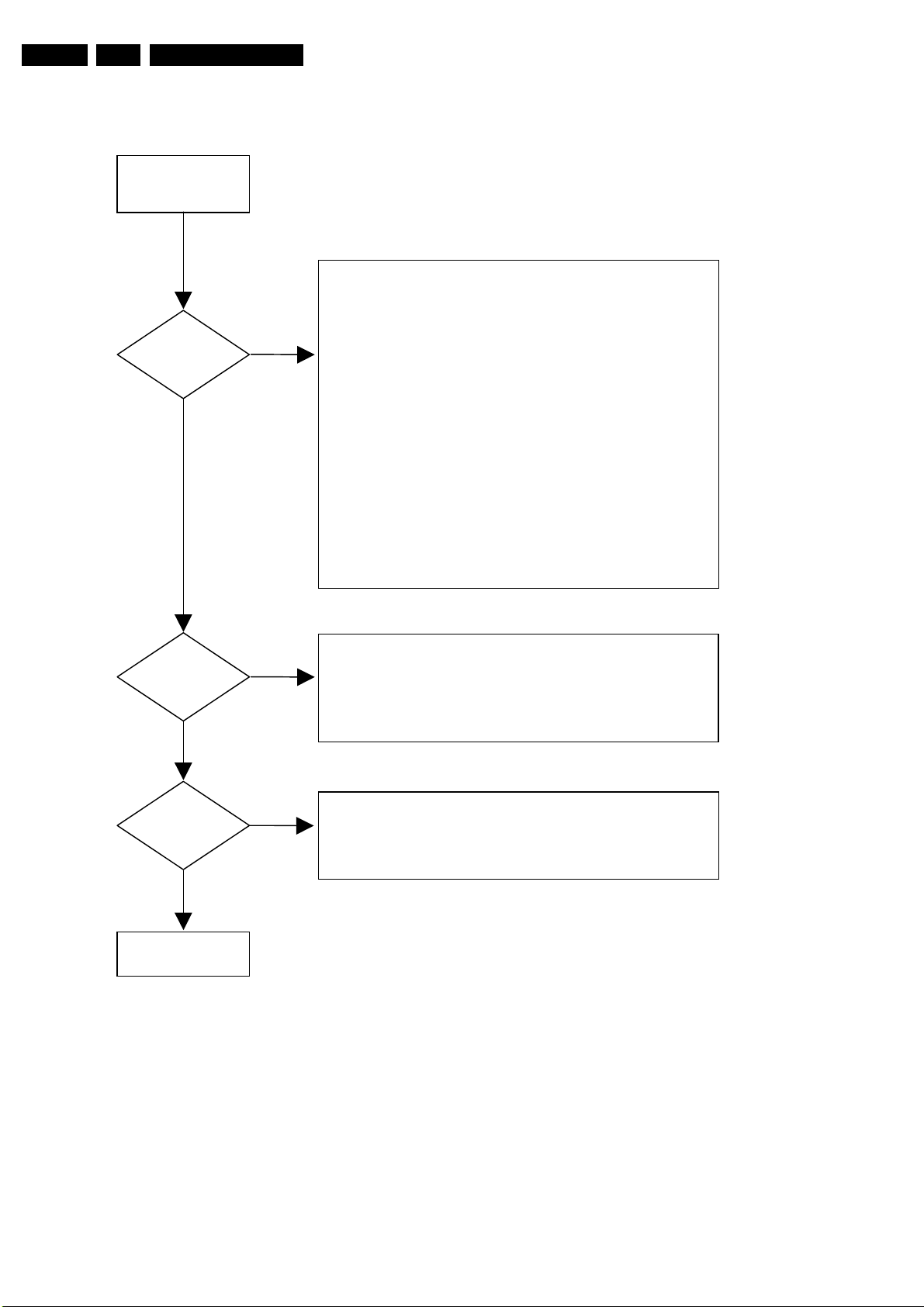
GB 58 CDR7798.
8.1.3 Display board troubleshooting guide
SWITCH POWER ON,
EXIT STAND BY
MODE
Faultfinding Guide
CHECK :
DISPLAY?
YES
KEY
FUNCTIONS?
YES
NO
NO
• SUPPLY VOLTAGES
⇒ -38V ±5% at conn. 1119-2
⇒ 3V8 ± 10% between conn. 1119-1 and 1119-3
⇒ +5V ± 5 % at conn. 1119-10 (1121-4 for CDR570/930)
• CLOCK SIGNAL
⇒ 8Mhz at pins 8, 9 of IC7104
• CONTROL SIGNALS
⇒ RESETN 3V3 (high) at conn.1119-4 after start up
⇒ I2C DATA at conn. 1119-5
⇒ I2C CLK at conn. 1119-7 (1121-1 for CDR570/930)
• FTD DRIVE LINES
⇒ Filament voltage 3V8 ± 10% between pins 1-2-3 and
pins 45-46-47 (pins 1-2 and pins 48-49 for CDR
570/930) of the FTD (1113)
⇒ Grid lines (see test instructions)
⇒ Segment lines (see test instructions)
• ELECTRICAL SERVICE DIAGNOSTICS - Local display test
CHECK:
• KEY MATRIX LINES (see test instructions)
• ELECTRICAL SERVICE DIAGNOSTICS – Keyboard test
• EASY JOG KNOB (see test instructions)
REMOTE
CONTROL?
YES
DISPLAY BOARD
OK
NO
CHECK:
• IR RECEIVER signal at pin 22 of IC7104 (see test instructions)
• ELECTRICAL SERVICE DIAGNOSTICS – Remote control test
Figure 8-9 ‘Display board troubleshooting’
CL 96532076_020.eps
290799
Page 59
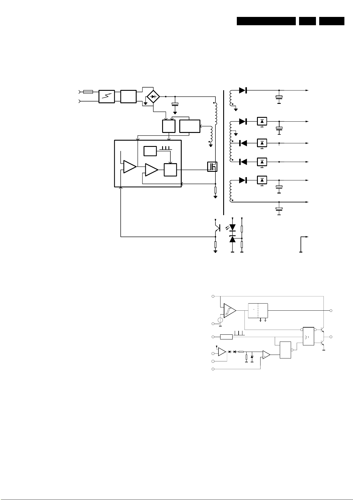
8.2 Circuit description of the current mode
power supply
8.2.1 Blockdiagram
Faultfinding Guide
GB 59CDR779 8.
MAINS
Lightning
Protection
EMI
FILTER
Comp
Error
Amplifier
+
-
Vfb
Verror
Rectifier
CLOCK
PWM
comparator
+
CONTROL
Start
Circuit
v
RQ
S
latch
Vcc
t2.5V
2643
Overvoltage
Protection
Output
Isense
7
9
7125
Vsense
Rsense
Vcc
+12V
6210
+5V
6230
+12V
6240
-8V
6250
VFTD
6220
VDC2
VDC1
+5V
0V
5131
2
5
7131
7201
8.2.2 Function description
MOSFET 7125 is used as a power switch controlled by the
controller IC 7110. When the switch is closed, energy is
transferred from mains to the transformer. This energy is
supplied to the load when the switch is opened. Through
control of the switched-on time, the energy transferred in
each cycle is regulated so that the output voltages are
independent of load or input voltage variations. The
controlling device UC3842 is an integrated pulse width
modulator. A clock signal initiates power pulses at a fixed
frequency. The termination of each output pulse occurs when
a feedback signal of the inductor current reaches a threshold
set by the error signal. In this way the error signal actually
controls the peak inductor current on cycle-by cycle basis.
8.2.3 Description of UC3842
The input voltage Vcc(pin 7) is monitored by a comparator
with hysteresis, enabling the circuit at 16V and disabling the
circuit below 10V. The error amplifier compares a voltage
Vfb(pin 2) related to the output voltage of the power supply,
with an internal 2.5V reference. The current sense
comparator compares the output of the error amplifier with
the switch current Isense(pin 3) of the power supply. The
output of the current sense comparator resets a latch, which
is set every cycle by the oscillator. The output stage is a
totem pole, capable of driving a MOSFET directly
Figure 8-10
8.2.4 Start up sequence
GND
Vfb
COMP
I sense
7
VI
16V
5
4
2
1
3
REGULATION
6V
+
-
+
OSCRt/ct
2.5V
ERROR AMP I SENSE COMP
+
-
S/R
2R
R1V
2.5V
REF
-
+
5V
BIAS
CL 06532151_018.eps
S
R
LATCH
271100
1
Figure B : Blockdiagram UC3842
Figure 8-11
t1: Charging the capacitor at Vcc
C2129 wiil be charged via R3123 and R3134, C2133 and
C2111 via R3129. The output is switched off
During t1.
t2: Charging of output capacitors
When the input voltage of the IC exceeds 14,5V, the circuit is
enabled and starts to produce output pulses. The current
consumption of the circuit increases to about 17mA,
depending on the external loads of the IC. At first, the
8
Vref
6
OUTPUT
CL 06532151_019.eps
271100
Page 60
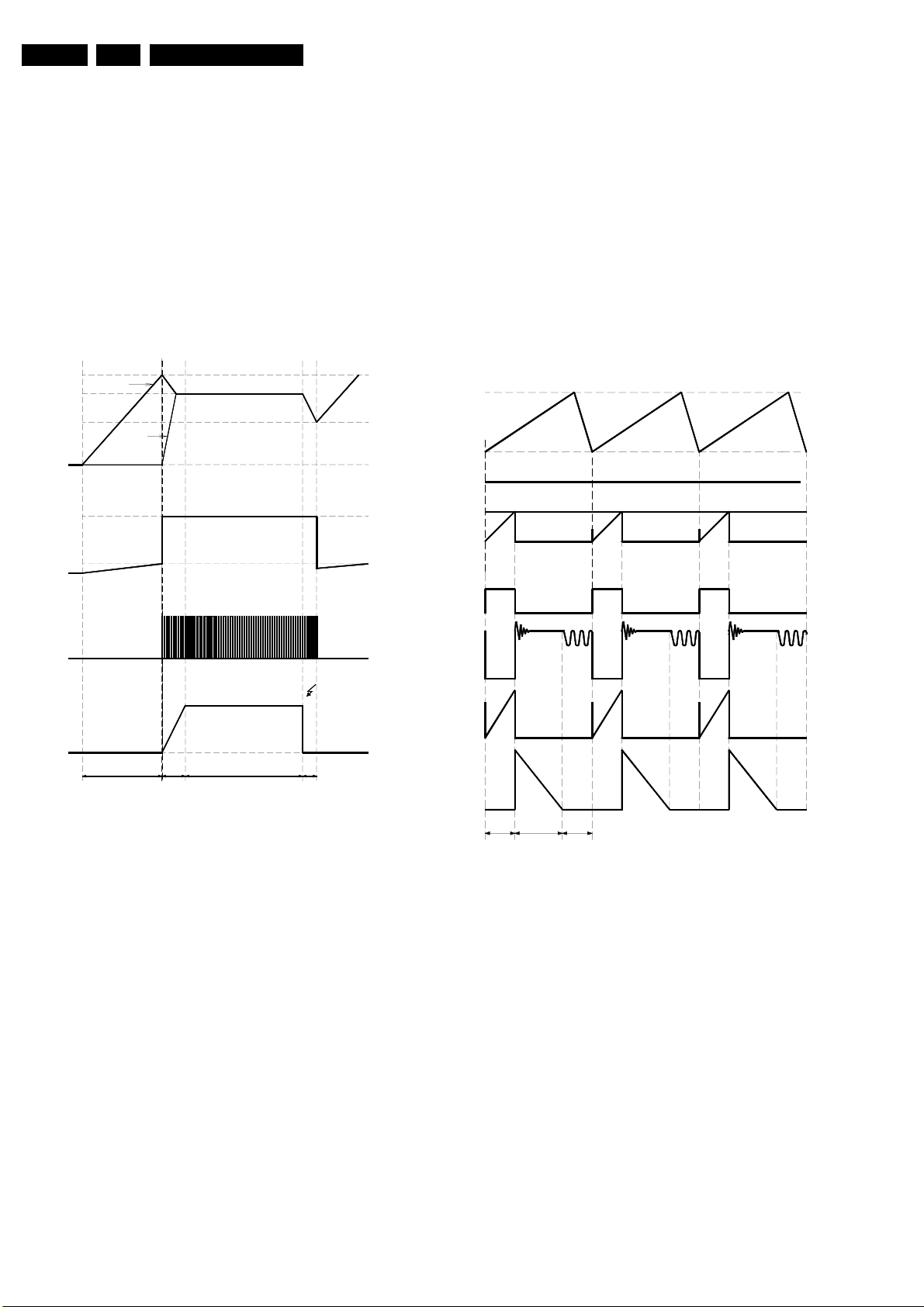
GB 60 CDR7798.
Faultfinding Guide
capacitor at the Vcc pin will discharge because the primairy
auxiliary voltage, coming from winding7-9 is below the Vcc
voltage. At some moment during t2, the primary auxiliary
voltages reaches the same level as Vcc.
This primary auxiliary voltage now determines the Vcc
voltage
t3: regulation
The output voltage of the power supply is in regulation
t4: overload
When the output is shortened, the supply voltage of the
circuit will decrease and after some time drop below the
lower threshold voltage. At that moment, the output will be
disabled and the process of charging the Vcc capacitor starts
again. If the output is still shorted at the next t2 phase, the
complete start-and stop sequence will repeat. The power
supply comes in a hiccup mode.
16V
Vcc
12V
10V
Vc2134
0V
20mA
Icc
1mA
becomes reversed. This results in a current flow through the
tranformer’s secondary winding via the diodes, electrolytic
capacitors and the load. This current is also ramp shaped but
decreasing.
TimeDEAD phase : when the stored energy has been
supplied to the load, the voltage from the secondary windings
falls below the output voltage(held constant by the
electrolytic capacitors) plus the threshold voltage of the
diodes. The current in the secondary winding stops flowing.
At this point, the drain voltage of the MOSFET is not yet zero
because C2609 between drain and source contains a certain
charge. This charge will start a sine-shaped ringing together
with the transformer’s self-induction.
The oscillator will start a next cyclus which consists of the
described three phases. The time of the different phases
depends on the mains voltage and the load.
TimeDEAD is maximum at an input of 400VDC and minimum
load, it will be zero at an input of 100VDC and overload.
V2
Vosc
V1
0
Vcomp
Vsense
OUTPUT
short
Vo
0
t1
t2 t3 t4
Figure C : Start-up sequence
CL 06532151_020.eps
Figure 8-12
8.2.5 Regulation
Figure 4 shows the most relevant signals during the
regulation phase of the power supply.
The oscillator voltage ramps up and down between V1 and
V2. The voltage at the current sense terminal is compared
every cycle with the output of the error amplifier Vcomp. The
output is switched off when the current sense level exceeds
the level at the output of the error amplifier.
TimeON phase : A drain current will flow from the positive
supply at pin 1 through the transformer’s primary winding, the
MOSFET and Rsense to ground. As the positive voltage at
pin 1 of the transformer is constant, the current will increase
linearly and create a ramp dependent on the mains voltage
and the inductance of the primary winding. A certain amount
of energy is stored in the transformer in the form of a
magnetic field. The polarity of the voltages at the secundary
windings is such that the diodes are non-conducting.
TimeDIODE phase : When the MOSFET is switched off,
energy is no longer supplied to the tranformer. The
inductance of the tranformer now tries to maintain the current
which has been flowing through it at a constant level. The
polarity of the voltage from the transformer therefore
271100
Vgate
Vdrain
Idrain
Idiodes
Ton Tdiode Tdead
Figure 8-13
CL 06532151_021.eps
271100
Page 61
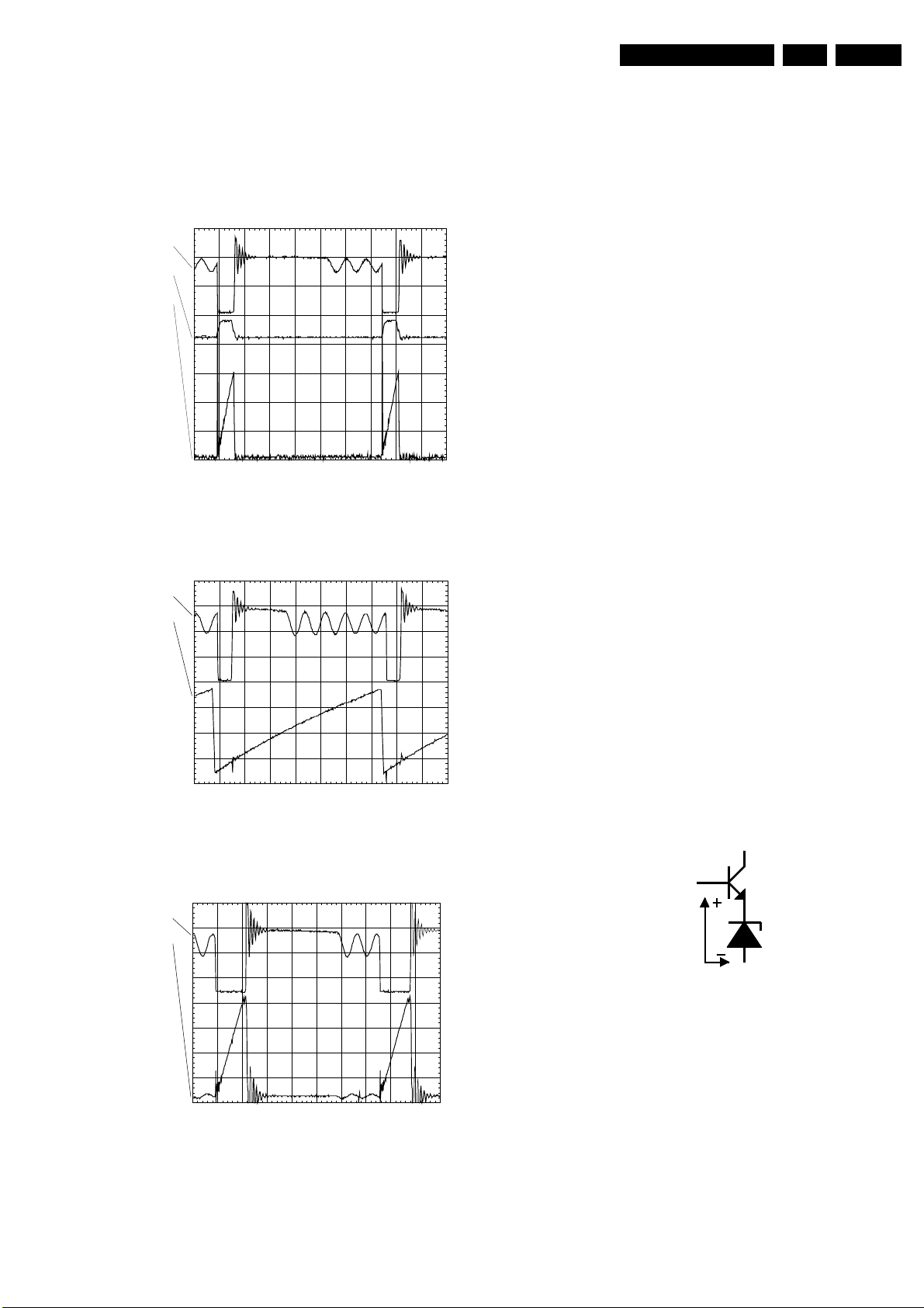
Faultfinding Guide
GB 61CDR779 8.
8.2.6 Oscillograms
Oscillograms
PM3394B
ch1
1
ch3
T
ch2
3
2
ch1 : Drain voltage
ch2 : Drain current
ch3 : Gate voltage
PM3394B
ch1
ch3
1
T
CH1 2
CH2
CH3 2 V~ ALT MTB5.00us- 0.90dv ch1-
CH1 1
CH3 50mV~ ALT MTB5.00us- 0.90dv ch1-
8.2.7 Circuit description
Input circuit
The input circuit consists of a lightning protection circuit and
an EMI filter.
The lightning protection comprises R3120, gasarrestor 1125
and R3124.
The EMI filter is formed by C2120, L5120, C2125 and R3124.
It prevents inflow of noise into/from the mains.
Primary rectifier/smoothing circuit
The AC input is rectified by rectifier bridge 6102 and
smoothed into C2121. The voltage over C2121 is
approximately 300V. It can vary from 100V to 390V.
Start circuit and Vcc supply
This circuit is formed by R3123, R3134, C2129, D6129,
R3129, R3111, C2133 and C2111.
When the power plug is connected to the mains voltage, the
stabilised voltage over D6129(24V) will charge C2133 via
R3129. When the voltage reaches 14,5V across C2111, the
control circuit of IC7110 is turned on and the regulation
starts. During regulation, Vcc of IC7110 will be supplied by
the rectified voltage from winding 7-9 via L5132, D6132 and
C2133.
Control circuit
The control circuit exists of IC7110, C2102, C2104, C2107,
C2109, C2110, R3102, R3103, R3104, R3107, R3108,
R3109 and R3110. C2102 and R3110 define the frequency
of the oscillator.
Power switch circuit
This circuit comprises MOSFET 7125, Rsense 3126, 3127
and 3128, R3125, C2127, L5125, R3112 and R3113. R3125
is a pull-down resistor to remove static charges from the gate
of the MOSFET.
3
ch1 : Drain voltage
ch2 : Oscillator voltage
CH1 1
CH3 20mV~ ALT MTB5.00us- 0.90dv ch1-
ch1
ch3
PM3394B
1
T
3
ch1 : Drain voltage
ch3 : Sense voltage
Figure 8-14
CL 06532151_022.eps
301100
Regulation circuit
The regulation circuit comprises opto-coupler 7200 which
isolates the error signal from the control IC on the primary
side and a reference component 7201. The TL431(7201) can
be represented by two components:
• a very stable and accurate reference diode
• a high gain amplifier
K
R
2.5V
A
CL 06532151_023.eps
Figure 8-15
TL431 will conduct from cathode to anode when the
reference is higher than the internal reference voltage of
about 2.5V. If the reference voltage is lower, the cathode
current is almost zero.
The cathode current flows through the LED of the optocoupler. The collector current of the opto-coupler flows
through R3106, producing an error voltage, connected to
voltage feedback pin 14 of IC7110.
271100
Overvoltage protection circuit
This circuit consist of D6114, C2114, R3115and R3116.
Page 62
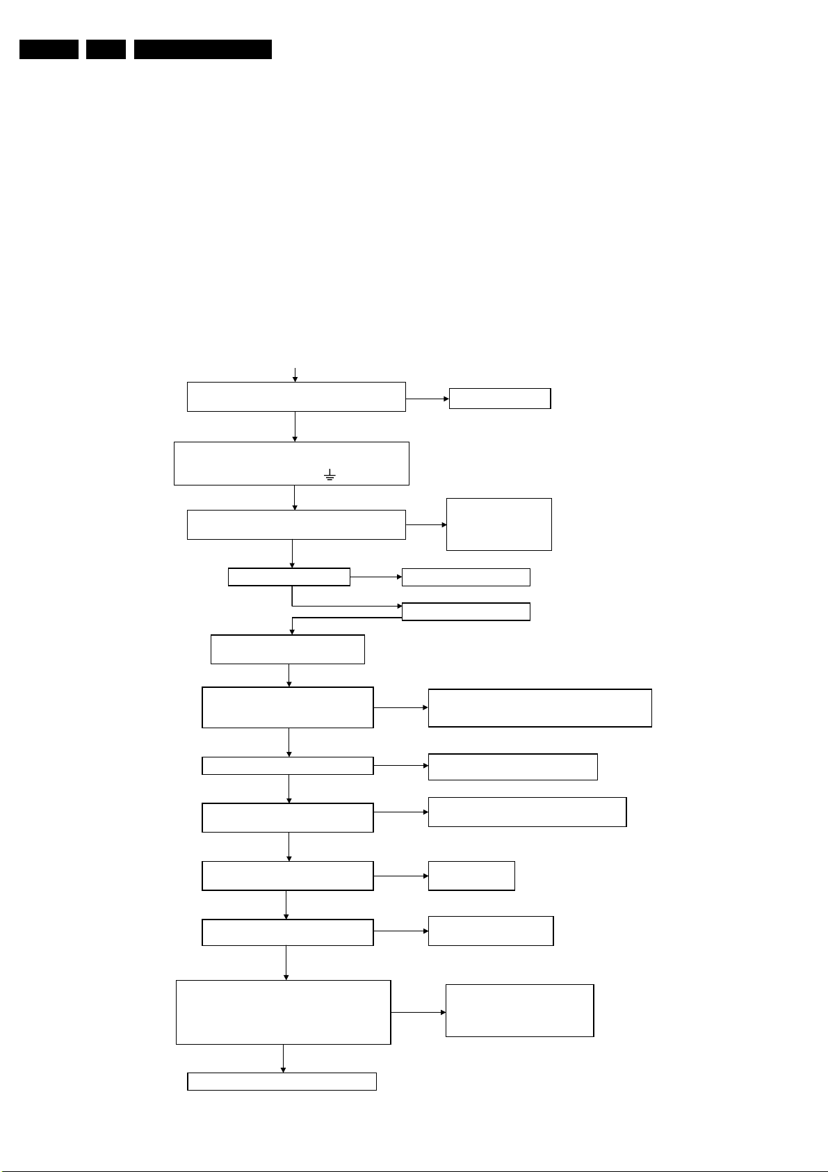
GB 62 CDR7798.
K
K
K
K
K
K
)
Faultfinding Guide
When the regulation circuit is interrupted due to an error in
the control loop, the regulated output voltage will increase
(overvoltage). This overvoltage is sensed on the primary
winding 7-9. When an overvoltage longer than 2.0µs is
detected, the output is disabled until Vcc is removed and then
re-applied. The power supply will come in a hiccup mode as
long as the error in the control loop is present.
8.2.8 Troubleshooting PSU CDR3-ECO
Faultfinding diagram
TROUBLE SHOOTING POWER SUPPLY
Check DC voltages
+5V +12V -8V VFTD(-38V) VDC1-VDC2(3V8)
Disconnect the power supply from the MAIN Board
Connect a dummy load resistor 6,8 ohm 10W (min 5W)
on the 5V and
NO
Secondary rectifier/smoothing circuit
There are 5 rectifier/smoothing circuits on the secondary
side. Each voltage depends on the number of windings of the
transformer.
The -8V supply is regulated by voltage regulator 7249.
On/off circuit
In off mode pin 1 and pin 2 of connector 0206 are connected.
The high voltage (-8V, +12V) over opto coupler 7200 forces
this one to conduct . IC 7110 is switched off
OK
power supply OK
+5V +12V -8V VFTD(-38V) VDC1-VDC2(3V8)
Check DC voltages
NO
Check the +5V
NO
OK
OK
connect the mains inlet to a mains
isolated variac
turn input voltage up and check across
C2121 the voltage
this voltage should be +/- 1,41 x Vin ac
OK
is power supply ticking?
NO
check Vcc on pin 7 IC7110
Vcc = 12V...... 16V
OK
check oscillator on pin 4 IC7110
is the osc +- 30kHz working ?
OK
check the voltage on the source of 7125
Vsource = 1,3V ?
NO (Vsource = +- 0.8V
power supply OK
OK
check - main board
check the fault voltage path
check 6210-2210-2253-5210
NO
check the functionality of the following components:
1120-2121-2125-2126-2127-6102-7125
YES
check the load on the secundairy output
check overload circuit 6141-7141-7150
NO
check 2121-2133-2134-3123-3134-6130-6132
replace 7110
NO
check 2102 - 3102
replace 7110
check 3125-3126-3127-3128
YES
replace 7125
- front board
- modem board
Disconnect diode 6150
start variac from 0V and turn-up slowly
measure the 5V output
If the 5V becoming higher than 5V, the regulator
circuit are damaged
5V OK
After the power repaired check the 3,3V
5V NOK
check:3201-3202-3203-3204-3205
3206-3207-3208-7131-7201
replace 7110
check circuit around Ic7110
CL 06532151_024.eps
271100
Figure 8-16
Page 63
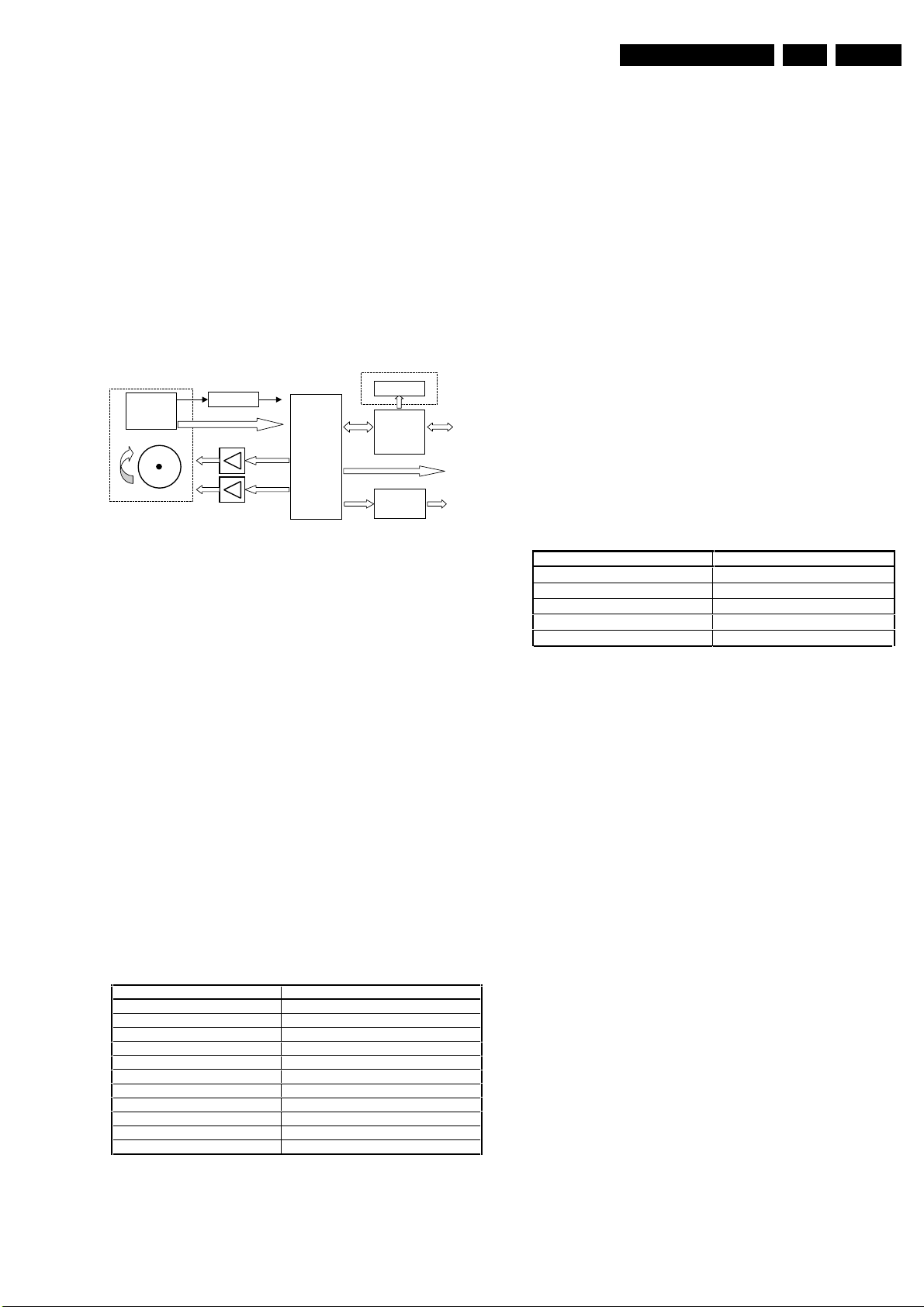
Faultfinding Guide
GB 63CDR779 8.
8.3 CD Main Board
The CD main board is built around the compact disc
mechanism VAM1250 and a loader 1250. The CDM delivers
diode signals and an unequalised high frequency signal.
These signals are necessary inputs for the decoder CD10.
Based on these signals the decoder will control the disc. The
decoder is able to control the sledge, focus motor, radial
motor and turn table. When everything is "locked", the
decoder delivers a digital output according to IEC958
standard, subcode to the microprocessor and I2S for
reproducing analog audio signals by means of a D/A
converter.
The microprocessor controls the CD10 and is slave of the
master processor on the CDR main board in the CDR779.
Both processors communicate via a DSA connection (data,
strobe and acknowledge).
CDM VAM1250
Trigenta
HF ampl.
Diode signals
Radial, focus
Motor, sledge
CD10
SERVO
DECODER
Loader assy
PROCESSOR
UDA1320
DAC
DSA
IIS, DOBM
ANA OUT
CL96532086_048.eps
080999
8.3.2 Clock Signals
Description
The microprocessor has its own Xtal or resonator of 12MHz.
The CD10 needs a clock of 8.4672MHz + 100ppm. This
speed also relates to the disc speed. To avoid locking
problems between the two drives in the CDR779, both drives
run on the same clock. Therefore the CD main board gets the
clock for the decoder from the CDR main board via pin 2 of
connector 1208.
The DAC needs a system clock to drive its internal digital
filters and to clock the I2S signals from the decoder. In our
case this is 11.2896MHz (CL11) generated by the CD10.
Measurements
• Connect the power supply as described above in "1.1.1.
Supply Voltages".
• Connect on pin 2 of position 1208 a clock signal of
8.4672 MHz ( 100ppm minimum rise time of 50ns and at
TTL level (0V and +5V).
• Keep microprocessor 7202 in reset by forcing pin 7 at
position 1208 to +5V.
• Release the reset. Now, the processor will reset the
CD10 for at least 75µs.
• The output clock CL11 should be available now at pin 42
of the CD10.
Check the following frequencies :
Figure 8-17
8.3.1 Supply Voltages
Description
The CD main board receives +5V and +12V from the CDR
main board via respectively pin 16 and pin 15 of connector
1208. The +5V is split up into +5VHF and +5V. The +5VHF
is used mainly for the diode currents and the HF-amplifier.
The +5V is used for the digital part of the board. On the board
a +3V3 is made from the +5V for the decoder CD10 and an
A3V3 for the DAC UDA1320. The +12V is split up into A12V
for the audio output stage and +12V for the power drivers of
the CDM.
Measurements
Connect following supplies to next pins :
• +5V + 5% to pin 16 of connector 1208.
• +12V + 5% to pin 15 of connector 1208.
• Ground reference to pin 17 of connector 1208.
Keep microprocessor 7202 in reset by forcing pin 7 of
connector 1208 to +5V. Check the following voltages :
Point Voltage
Position 1000 pins 1,3
Position 7000 pins 5,17,21,57
Position 7005 pin 14
Position 7020 pins 25
Position 7020 pins 26,27,28
Position 7021 pin 5
Position 7022 pin 5
Position 7025 pin 16
Position 7202 pin 38
Position 7309 pins 4,13
Position 7120 pin 8
+5V ± 5%
+3.3V ± 5%
+5V ± 5%
+5V ± 5%
+10 ± 10%
+12V ±10
+12V ±10
+5V ± 5%
+5V ± 5% ( other appl. 3V3 possible)
+3V3 ± 5%
+12V ± 10
CL96532086_049.eps
080999
Point Frequency
Position 7000 pin 16
Position 7202 pins 14,15
Position 7309 pin 6
Position 7309 pin 1
Position 7309 pin2
8.4672 MHz ± 100ppm
12MHz ± 5%
11.2896 MHz ± 100ppm
2.1168 MHz ± 100ppm
44.1kHz ± 100ppm
Figure 8-19
8.3.3 CD10 Decoder/Servo SAA7324 (7000)
Description
The CD10 is a single chip combining the functions of a CD
decoder, digital servo and bitstream DAC. The decoder/
servo part is based on the CD7. The decoding part supports
a full audio specification and can operate at single speed
(n=1) and double speed (n=2).
CL96532086_050.eps
080999
Figure 8-18
Page 64
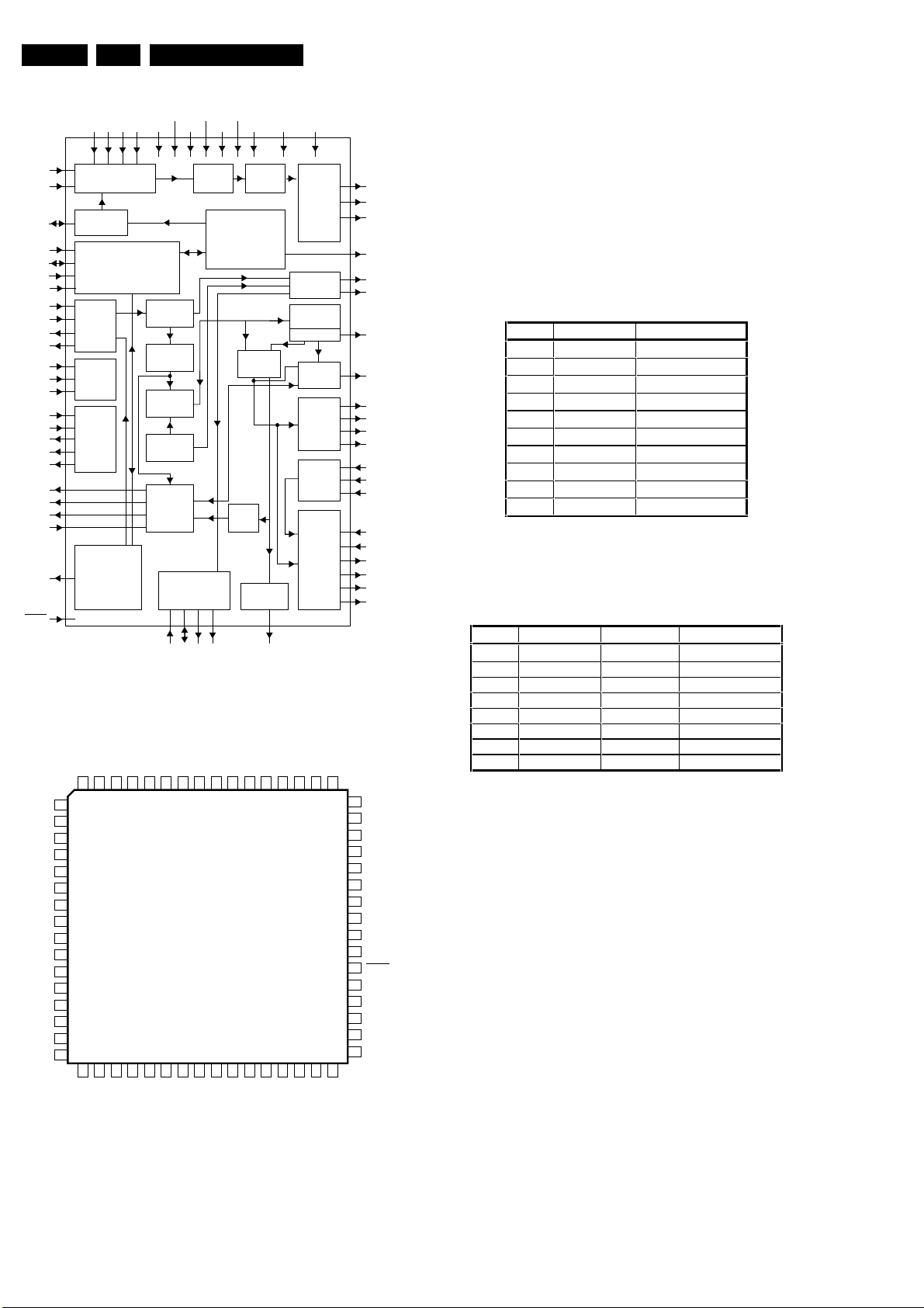
GB 64 CDR7798.
Faultfinding Guide
Block Diagram
12
R1
13
R2
7
V
RIN
40
SCL
39
SDA
41
RAB
42
SILD
2
HFIN
1
HFREF
3
ISLICE
6
I
ref
25
TEST1
31
TEST2
44
TEST3
24
SELPLL
16
CRIN
15
CROUT
26
CL16
49
CL11/4
48
SBSY
47
SFSY
46
SUB
45
RCK
43
STATUS
38
RESET
Pin Configuration
1
HFREF
2
HFIN
3
ISLICE
4
V
SSA1
V
5
DDA1
I
6
ref
V
7
RIN
D1
8
D2
9
D3
10
D4
11
R1
12
R2
13
V
14
SSA2
CROUT
15
CRIN
16
V
V
D1 D2 D3 D4
8910
ADC
V
ref
GENERATOR
MICROCONTROLLER
INTERFACE
FRONT
END
TEST
TIMING
DECODER
MICRO-
CONTROLLER
INTERFACE
SSA2
V
SSA1
4 14 5 17 33 50 58 52 57
11
DIGITAL
PLL
EFM
DEMODULATOR
SRAM
RAM
ADDRESSER
SUBCODE
PROCESSOR
VERSATILE PINS
INTERFACE
63 34 61 62 32
V1
V2/V3V4 V5 KILL
V
DDA1
DDA2
V
SSD1VSSD3
PRE-
PROCESSING
V
SSD2
CONTROL
PART
PROCESSOR
PEAK
DETECT
CONTROL
FUNCTION
AUDIO
KILL
V
DDD1(P)VDDD2(C)
OUTPUT
MOTOR
CONTROL
ERROR
CORRECTOR
FLAGS
INTERFACE
INTERFACE
(LOOPBACK)
INTERFACE
BITSTREAM
Figure 8-20
SSD3
DDD2(C)
FO
SL
V
LDON
64
V5
V1
62
63
MOTO1
V4
MOTO2
60
61
V
55
56
57
58
59
SAA7324
171819202122232425262728293031
pos
LP
neg
VDDA2
LN
V
RP
RN
V
SELPLL
TEST1
CL16
DDD1(P)
RA
54
DATA
CFLG
53
WCLK
V
52
SCLK
DOBM
514950
EF
Figure 8-21
54
55
STAGES
56
64
59
60
53
51
EBU
30
29
SERIAL
DATA
28
27
37
SERIAL
35
DATA
36
20
21
18
DAC
19
22
23
CL96532086_051.eps
080999
SSD2
CL11/4
V
48
47
46
45
44
43
42
41
40
39
38
37
36
35
34
33
32
KILL
TEST2
CL96532086_052.eps
080999
RA
FO
SL
LDON
MOTO1
MOTO2
CFLG
DOBM
EF
SCLK
WCLK
DATA
SCLI
WCLI
SDI
V
neg
V
pos
LN
LP
RN
RP
SBSY
SFSY
SUB
RCK
TEST3
STATUS
SILD
RAB
SCL
SDA
RESET
SCLI
SDI
WCLI
V2/V3
V
SSD1
8.3.4 TDA7073A Power Drivers (7021, 7022)
Description
The TDA7073A is a dual power driver circuit for servo
systems with a single supply. In this configuration it is used
to drive the sledge, tray, focus and radial.
Measurements
Keep microprocessor 7202 in reset by forcing pin 7 of
connector 1208 to +5V. Connect the power supply as
described above in "1.1.1. Supply Voltages". Check the
following voltages :
Pin Location Value
5 7021
5 7022
1 7022
2 7022
6 7022
7 7022
1 7021
2 7021
6 7021
7 7021
12V ± 10%
12V ± 10%
1.65V ± 10%
1.65V ± 10%
1.65V ± 10%
1.65V ± 10%
5.0 ± 10%
5.0 ± 10%
1.65V ± 10%
1.65V ± 10%
CL96532086_053.eps
Figure 8-22
Pin Location Value DC
9 7022 FOC
5.8V ± 10%
12 7022 FOC 5.8V
13 7022 RAD 5.8V
16 7022 RAD 5.8V
9 7021 SLE 5.8V
12 7021 SLE 5.8V
13 7021 TRAY- 5.8V
16 7021 TRAY+ 5.8V
CL96532086_054.eps
Figure 8-23
8.3.5 BA6856FP Turn Table Motor Driver (7020)
Description
This component is a 3 phase, full wave pseudo linear driving
system with inbuilt Hall Bias circuit and 3 phase parallel
output.
Measurements
Keep processor 7202 in reset by forcing pin 7 of connector
1208 to +5V. The outputs 9, 10, 11 of connector 1006 are 0V.
Pin 21 of the motor driver 7020 is 2.5V ( 10%.
Pin 22 of the motor driver 7020 is 2.5V ( 10%.
Pin 23 of the motor driver 7020 is 0V.
Pin 19 of the motor driver 7020 is 5V ( 10%.
Put the processor out of reset to continue the measurement.
Check MOT1 at pin 59 of CD10. The duty cycle of the output
should be 50%. Check wave form at pin 11 of 7005-D :
amplitude 5V + 5% duty cycle 50%.
The motor driver 7020 can be measured dynamically by
connecting a hall motor to the application panel. Apply a
pulse of 1V 10Hz and 15% duty cycle to pin 22 (Ec) as input
value with reference to pin 21 (Ecr=2.5V). Measure the
output signals on the driver. This will give as response a
square wave on pin 17 and pin 18. When a positive voltage
080999
080999
Page 65
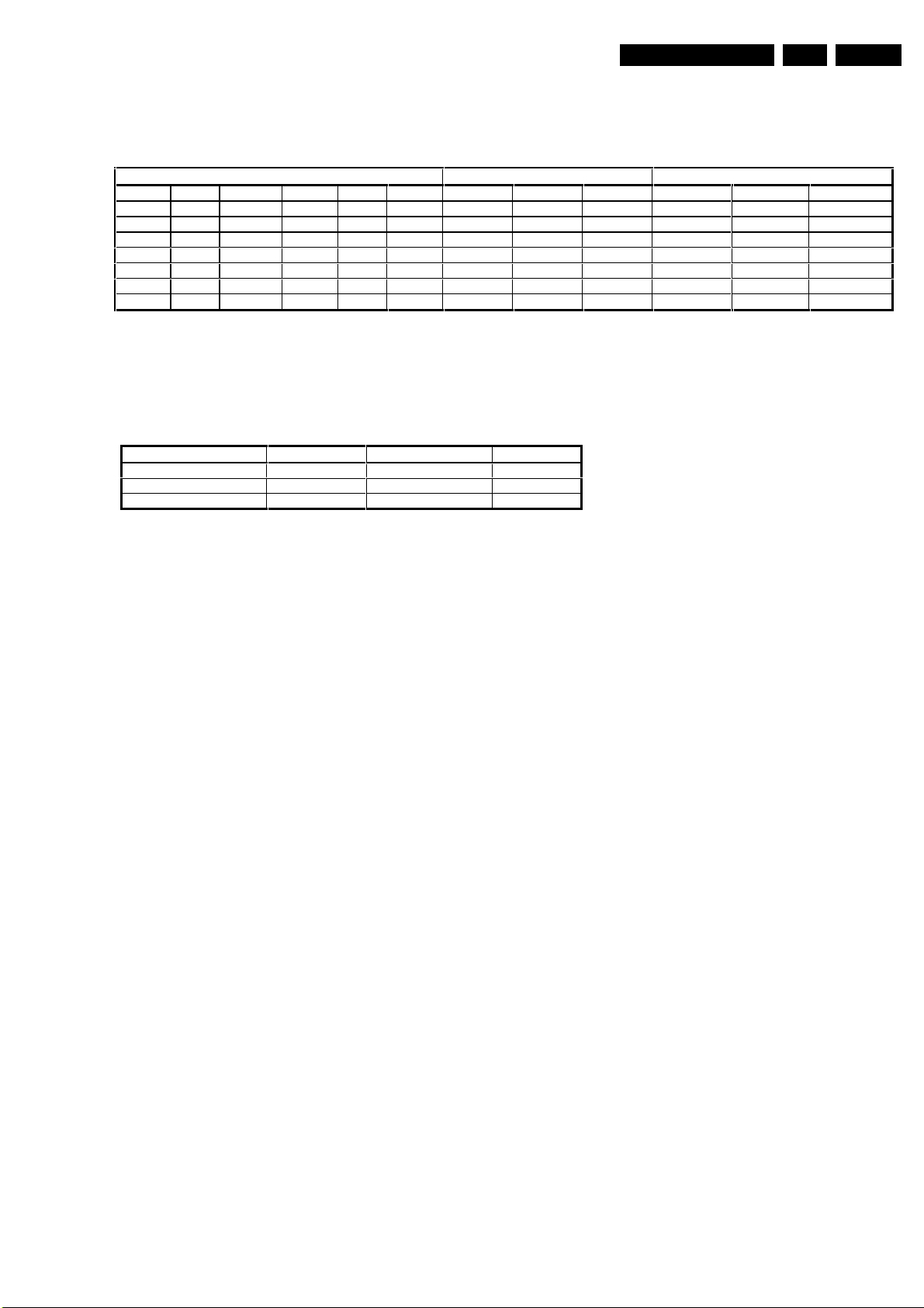
Faultfinding Guide
GB 65CDR779 8.
is applied, the square wave on pin 17 will go ahead of the
square wave on pin 18.
All signals will have a value as shown in the truth table.
Check the following output signals :
Motor controller truth table
Input conditions conn 1006 pin Outputs conn 1006 Test points on driver
684 732 9 10 11 18 17 16
U+ U- V+ V- W+ W- UCOIL VCOIL WCOIL HALL_U HALL_V HALL_W
L M H M M M 6V 0V 0V 0V 5V
H M L M M M 0V 6V 6V 5V 0V
M M L M H M 0V 6V 0V 0V 5V
M M H M L M 6V 0V 6V 5V 0V
H M M M L M 0V 0V 6V 5V 0V
L M M M H M 6V 6V 0V 0V 5V
Figure 8-24
CL96532086_055.eps
080999
Hall-elements input signal voltage
levels
Input voltage Level Tolerance Unit
H2.80.1V
M2.50.1V
L2.20.1V
CL96532086_056.eps
080999
8.3.6 Tray Control
Description
The tray control consists of a TDA7073A power driver (7021)
controlled by the processor 7202 via pin 19 TRAYIN and pin
20 TRAYOUT. If pin 20 is low and pin 19 high, the TRAY+
signal at pin 16 of 7021 is forced to +8V and the TRAY- signal
at pin 13 of 7021 to GND : the tray will open. If pin 20 is high
and pin 19 low, TRAY+ becomes GND and TRAY- becomes
+8V : the tray will close. If pin 19 and 20 of the processor
have the same value, TRAY+ and TRAY- will have the same
value as well : the tray stops moving.
Measurements
Keep procesor 7202 in reset by forcing pin 7 of connector
1208 to +5V. Connect a load of 15Ω, 7W between pin 3 and
4 of connector 1002. Check the voltage over the load with
TRAY+ (pin 3) as positive reference. Check also the levels of
pins 19 and 20 of the processor.
U TRAY+,TRAY- = <100mV
Pin 20 = +5V
Pin 19 = +5V
Force pin 20 of the processor to ground, and check the
voltages.
U TRAY+,TRAY- = -6.5V( 10%
Pin 20 = +0V
Pin 19 = +5V
Force pin 19 of the processor to ground as well and check the
levels again.
U TRAY+,TRAY- = <100mV
Pin 20 = +0V
Pin 19 = +0V
Release pin 20 of the processor and check the levels.
U TRAY+,TRAY- = 6.5V( 10%
Pin 20 = +5V
Pin 19 = +0V
Release pin 19 of the processor and check the levels again:
U TRAY+,TRAY- = <100mV
Pin 20 = +5V
Pin 19 = +5V
Figure 8-25
Page 66
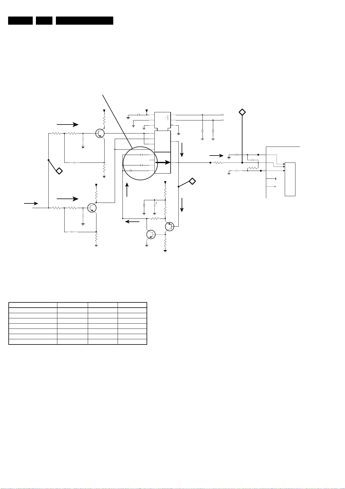
GB 66 CDR7798.
Faultfinding Guide
8.3.7 HF Path
Description
The pre-amplified HF-signal is presented to both n=1 and
n=2 amplifier circuits. The mux/demux switches via software
and micro processor controlled S1 and S2 lines between
either one of the amplified n=1 or n=2 signals. The signal will
n-dependant filtering
+5VHF
PRE AMP
HF
3173
430R
F157
n=2 AMP
3191
430R
n=1 AMP
3174
430R
2143
330p
2
3192
430R
2164
180p
2140
HFGND
2162
HFGND
180p
100p
+5VHF
3188
3203
2K7
7009
BFS20
2K7
HFGND
3169
7023
BFS20
3180
HFGND
2K7
2K7
HFGND
DUAL 4 CHANNEL
MUX/DEMUX
+5VHF
HFGND
2141
2n2
2146
1n5
16
7
8
1
5
2
4
12
14
15
11
74HCT4052D
VCC
VEE
GND
0
1
2
3
+5VHF
HFGND
390p
2149
680p
2130
100n
HF
47u
22n
2160
HFGND
HFGND
HF
BC848B
7010
HFGND
1K
3196
BC858B
7007
4x
3189
2161
3193
3205
HFGND
then follow another amplification and filtering circuit. The
filtering again is controlled by the S1 and S2 lines, dependant
on whether the disc starts up (speed n=1, S1 and S2 Low),
disc plays at speed n=1 (S1 Low, S2 High) or disc plays at
speed n=2 (S1 and S2 High).
7025
0
3
G4
0
1
390R
10
9
6
HFGND
3
13
F313
22n
HFGND
HF
F156
9
22n
2137
HFGND
HFIN
3178
2138
1K
S1
S2
HFGND
HFGND
2142
22n
2150
47n
F310
3
7000
SAA7324
F309
1
HFREF
2145
2
3181
22K
F159
3
4
5
HFIN
ISLICE
VSSA1
VDDA1
47p
HF
180R
10K
CL96532086_057.eps
FRONT
END
080999
DC Settings
Set the power and reset connections as described above in
"1.1.1. Supply Voltages". Check the following voltages :
Force Pin Location Measure
Emitter 7006 2.4 ± 10%
S1 and S2 “HIGH” Collector 7010 1.9 ± 10%
S1 and S2 “LOW” Collector 7010 1.9 ± 10%
S1 and S2 “HIGH” 13 7025 1.6 ± 10%
S1 and S2 “LOW” 13 7025 1.6 ± 10%
S1 and S2 “HIGH” 3 7025 3.2 ± 10%
S1 and S2 “LOW” 3 7025 3.2 ± 10%
CL96532086_058.eps
Figure 8-27
Figure 8-26
080999
Page 67
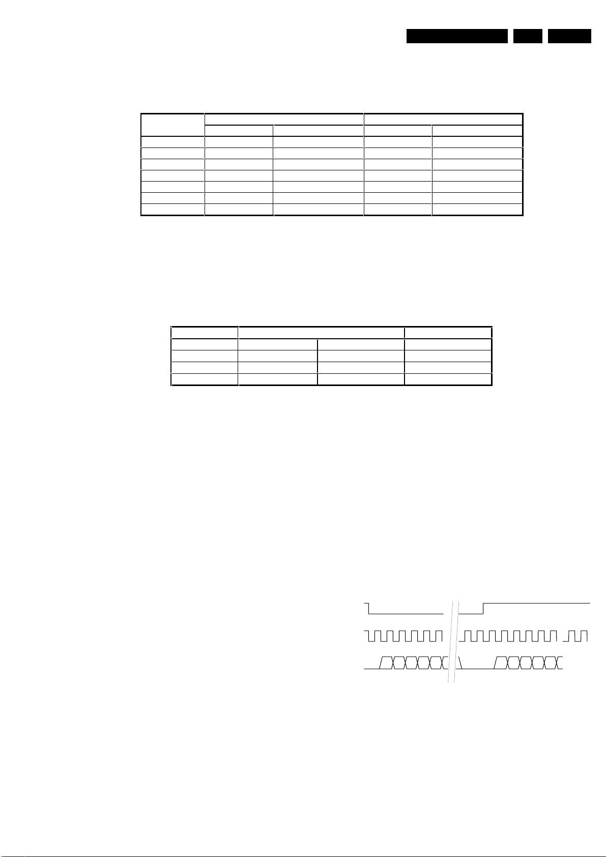
Faultfinding Guide
GB 67CDR779 8.
Transfer Characteristics
Set the power and reset connections as described above in
"1.1.1. Supply Voltages". Connect a function generator via a
serial resistor of 1k5 to pin 4 of connector 1000. Use the
S1 and S2 “low” S1 and S2 “high”Frequencies
Input V
AC
Pin 2 at 7000 Input V
300 Hz 200mV < 100mV ± 20% 200mV < 100mV ± 20%
10 kHz 200mV 295mV ± 20% 200mV 330mV ± 20%
100 kHz 200mV 310 mV ± 20% 200mV 330 mV ± 20%
300 kHz 200mV 385 mV ± 20% 200mV 335 mV ± 20%
800 kHz 200mV 655 mV ± 20% 200mV 485 mV ± 20%
1.5 MHz 200mV 1.1V ± 20% 200mV 760 mV ± 20%
3MHz 200mV 1.1V ± 20% 200mV 1.1V ± 20%
HFDET Setting
Set the power and reset connections as described above in
"1.1.1. Supply Voltages". Connect a function generator via a
serial resistor of 1k5 to pin 4 of connector 1000. Use the
Location Voltage DC Voltage AC
No HF HF
F190 4.8V± 20% 4.8V± 20% 175mV± 20%
F192 < 100mV 1.1V± 20% F206 4.9V± 20% 150mV± 20% -
Figure 8-28
function generator as a sine wave generator with output level
of 1Vtt. Check this AC value with an AC mV-meter connected
to the input (pin 2) of the CD10 (7000) :
AC
Pin 2 at 7000
CL96532086_059.eps
080999
function generator as a sine wave generator with output level
of 500 kHz, 1Vtt. Check this AC value with an AC mV-meter :
CL96532086_060.eps
080999
8.3.8 Audio Part - DAC
Description
The DAC used, is the UDA1320 bit stream, continuous
calibration. I2S signals from various formats can be entered
at pins 1,2 and 3. If these signals are in phase with the
delivered system clock at pin 6, the DAC will reproduce
analog output signals at pins 14 and 16. 0dB level is
0.85Vrms. These analog signals are at 1.65Vdc level.
The DAC has features which can be checked on the input
pins. Mute will switch off the analog signals. De-emphasis is
not used, since this is done in the decoder. Attenuation of 12dB is not used because this is also done in the decoder.
I2S
I2S is a kind of digital audio format, consisting out of 3 lines :
CLOCK, WORDSELECT and DATA.
WORD-SELECT
Word select (WS) indicates whether the data-sample is from
the left or the right audio-channel. It has the same frequency
as the sample rate of the digital audio signal. This can be 32,
44.1 or 48kHz. Normal polarity is low for a left sample and
high for a right sample. So within the low state of the WS-line
the data bits for the left channel are transferred, and within
the high state the data bits of the right channel are
transferred.
Figure 8-29
WS
CLK
DATA
Transition of the WS always happens on a falling edge of the
CLK.
DATA
transmitting device, and read by the receiving device. The
position of the DATA-bits within the WS-signal is very
important. There are several formats for this. In our case we
always use Philips I2S format, no Japanese or Sony format.
The number of data-bits per channel depends on the used
devices.
Timing of the I2S-bus, in case of Philips I2S is shown in the
next figure :
LEFT SAMPLE RIGHT SAM PLE
MSBMSB
CL96532086_061.eps
080999
Figure 8-30
CLOCK
The CLOCK signal (CLK) indicates when DataTips must be
set, and when DataTips must be read. The frequency
depends on the speed of the I2S-bus, but is always a factor
of the frequency of the WS-signal. It can be 48x, 64x, 96,
128x... .In our case it is 48x the sample rate frequency =
2.1168MHz. The signal is in phase with the WS-signal.
Page 68
GB 68 CDR7798.
Measurements
Faultfinding Guide
IIS
22
DAC AMPLIFIER
CLK11
25
NMUTE
Keep processor 7202 in reset by forcing pin 7 of connector
1208 to +5V. This puts the processor outputs in tristate.
Check the reset at pin 4 of processor 7202 to make sure that
the processor is in reset.
Now, force port 0-4 pin 33 at 7202 to 0V to set the decoder
outputs (SCLK, WCLK, DATA, and CL11).
Check the MUTE pin 11 at 7309 : this pin should be low.
Connect via an I2S generator I2S-signals to the DAC :
Pin 1 at 7309: SLCK.
Pin 2 at 7309: WCLK.
Pin 3 at 7309: DATA.
Connect also the SYSCLK pin 6 at position 7309 to a clock
signal of 11.2896 MHz ( 100ppm.
Generate an I2S signal equivalent with a sine wave of 1kHz
at 0dB for both left and right channels.
Check if 0.8 VRMS at pins 14 and 16 at location 7209 with a
DC of 1.65VDC.
Check if 1.7 VRMS ( 2 dB at connector pins 1and 3 at location
1209.
Force MUTE Pin 11 at 7309 high.
Measure again at pins 1 and 3 at location 1209 : both signals
should be at -90 dB.
Figure 8-31
1200 - 17
1200 - 19
CL96532086_062.eps
080999
Page 69
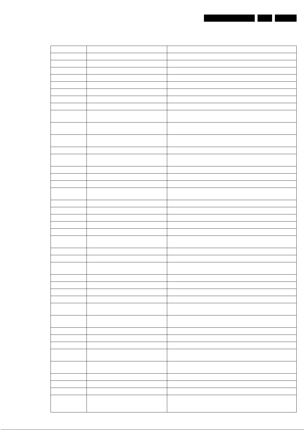
9. List of Abbreviations
SIGNAL NAME SIGNAL FLOW FUNCTION AND DESCRIPTION
+12V main supply voltage from PSU +12V supply voltage from PSU
+12VA supply voltage +12V supply voltage for Audio part
+5V main supply voltage from PSU +5V supply voltage from PSU
+5VA supply voltage +5V supply voltage for Audio part
+9SRVPWR IC7558 ->- IC7240 PoWeR supply for SeRVo driver IC
12VPWR supply voltage +12V supply voltage for servo part
-8V main supply voltage from PSU -8V supply voltage from PSU
-8VA supply voltage -8V supply voltage for Audio part
A(1:20) IC7701 -> R3818,R3819, R3820, R3821,
R3897 -> IC7703
A(10:20) IC7701 -> R3819, R3820, R3821 ->
IC7702
A1 IC7010 -> IC7270 amplitude of the “land” reflection relative to the average EFM, voltage
A1LF, A2LF CONN1000 -> IC7010 satellite photo diodes A1, A2 current output
A2 IC7010 -> IC7270 amplitude of the “pit” reflection relative to the average EFM, voltage
A-8V supply voltage -8V supply voltage for servo part
AEGER Analog Error signal GEnerator for Recordable
AINTON IC7008 -> IC7010 Alpha INTegrator ON (to AEGER)
ALE IC7270 -> R3213 -> IC7209,
IC7300IC7270 -> R3230
ALPHA0 IC7270 -> IC7010 analog voltage mode output from OPC D/A converter
ALS IC7008 -> IC7010 Alpha Loop Switch (to AEGER)
ASTROBE IC7008 -> IC7010 Alpha STROBE (to AEGER)
ATIP Absolute Time In Pre-groove (sync signal)
ATIPSYNC IC7300 -> IC7270 ATIP SYNC signal
ATT IC7270 -> R3717, R3722IC7270 ->
IC7701
B1LF, B2LF CONN1000 -> IC7010 satellite photo diodes B1, B2 current output
BCLK IC7701 -> R3898A -> IC7300 I2S1 BitCLocK from DASP to CDR60 (playback and record)
BE_RESET IC7701 -> R3261 -> IC7270IC7701 ->
R3716
BIASC IC7008 -> R3056 BIAS Current switch CDRW output
BKPT CONN1819, R3907 -> IC7701 JTAG mode select / debug mode BreaKPoinT
C1LF, .. , C4LF CONN1000 -> IC7010 Central photo diodes C1, C2, C3, C4 current output
CAGAIN R3016,R3115 -> IC7010 set-point laser power on disc, current input
CAHF CONN1000 -> C2374 Central Aperture (central photo diodes) High Frequency current
CALF IC7010 -> IC7270 Central Aperture (central photo diodes) Low-pass Filtered signal (DC
CAS0 IC7701 -> IC7702 Column Address Strobe DRAM for upper byte
CAS1 IC7701 -> IC7702 Column Address Strobe DRAM for lower byte
CDR IC7008 -> IC7355 CDR strategy detected output (active high)
CDR60CFLG IC7300 -> R3382B -> CONN1812 serial output of error corrector status information of the CDR60-
CDR60CL1 IC7300 -> R3382C -> CONN1812 output of CLock signal for testing system clock of IC CDR60 at test
CDR60CS IC7270 -> R3235B -> R3702, IC7300 CDR60 Chip Select, active high
CDR60INT IC7300 -> IC7270 CDR60 INTerrupt line, active low
CDR60LWRT IC7300 -> R3048 CDR60 Laser WRiTe control output
CDR60MEAS1 IC7300 -> R3382A -> CONN1812 serial output of information about jitter, PLL frequency and
List of Abbreviations
Address lines 1 to 20 between DASP and flash ROM
Address lines 10 to 20 between DASP and DRAM
output, OPC input
output, OPC input
Address Latch Enable; external address latch strobe line, freeze
address when low
ATTenuation request from MACE2 to audio DAC, active low; means
that the output can be attenuated in case of search activities
Basic Engine RESET, active high
output (C1+C2+C3+C4)
coupled EFM signal), voltage output, OPC input
decoder, to be measured at test connector
connector
asymmetry of bit recovery block in CDR60, to be measured at test
connector
GB 69CDR779 9.
Page 70
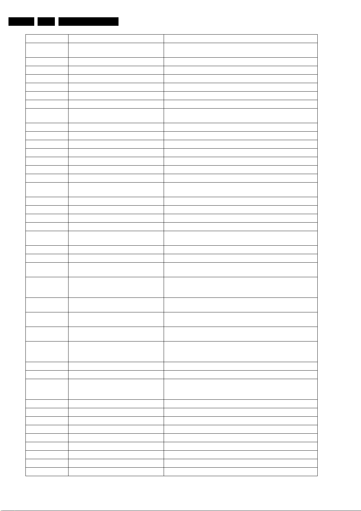
GB 70 CDR7799.
CDR60PLL IC7270 -> R3305 -> IC7300 CDR60 clock multiplier enable, active high
CDRW IC7355D -> IC7355CIC7355D ->
CONN1000
CLK_OUT IC7701 -> R3771 -> CONN1819 system CLocK OUT
CLK_SYS IC7701 -> R3727, R3731 oscillator output
COS- CONN1220 -> IC7225B Hall feedback signal from sledge motor
COS+ CONN1220 -> IC7225B Hall feedback signal from sledge motor
CSFLASH IC7701 -> IC7703 Chip Select for FLASH or boot device
CSRAM IC7270 -> R3235A -> R3703, IC7802 Chip Select SRAM, active low
D(16:31) IC7701 <-> R3822, R3823, R3824,
R3825 <-> IC7703, IC7702
D3V3 supply voltage +3,3V supply voltage for Digital part
D5V supply voltage +5V supply voltage for Digital part
D5VS supply voltage +5V supply voltage for Servo part
DALPHA IC7010 -> R3037 ALPHA error signal for laser power control
DASP Digital Audio Signal Processor
DATAI IC7701 -> R3898C -> IC7300 I2S1 DATA In from DASP to CDR60 (recording)
DATAO IC7300 -> R3314 -> IC7701 I2S1 DATA Out from CDR60 to DASP (playback)
DEEMP IC7270 -> R3719, R3724IC7270 ->
IC7701
DELTAP IC7016 -> R3126 DELTA Power current source drive signal from XDAC
DIG_OUT_C IC7701 -> R3706 -> C2707, CONN1400 Common DIGital OUTput (consumer)
DISPLAY_INT F934 -> R3812, IC7701 DISPLAY INTerrupt
DMON IC7270 -> R3324 power save at stop, active low
DOBM_CD CONN1708, C2731 -> R3757 -> R3903 -
> IC7701
DOBM_CDR IC7300 -> R3382D -> C2379, IC7701 Digital Output (EBU output) from CDR60 to DASP
DRAM_RW IC7701 -> IC7702 Read/Write strobe for DRAM
DSA_ACK_CD IC7701 <-> R3830 <-> R3831 <->
CONN1708IC7701 <-> R3830 <-> C2735
DSA_ACK_CDRIC7701 -> R3729 -> IC7270,
CONN1830IC7701 -> R3729 -> R3769
DSA_DATA_CD IC7701 <-> R3828 <-> R3829 <->
CONN1708IC7701 <-> R3828 <-> C2733
DSA_DATA_CDRIC7270<->R3246 <-> R3813 <-> IC7701,
CONN1830IC7270<->R3246 <-> R3767
DSA_STR_CD IC7701 <-> R3835 <-> R3832 <->
CONN1708IC7701 <-> R3835 <->C2734
DSA_STR_CDRIC7270 -> R3245 -> IC7701,
CONN1830IC7270 -> R3245 -> R3768
DSCLK CONN1819, R3908 -> IC7701 reset in / Debug Serial CLocK in
DSI CONN1819, R3909 -> IC7701 JTAG reset in / Debug Serial clock In
EFM Eight to Fourteen Modulation = modulation method used for CD
EFMCLK IC7300 -> IC7008 EFM CLocK output
EFMDATA IC7300 -> IC7008 EFM DATA output
EFMTIM3 EFM TIMing generator
EPON IC7008 -> R3010IC7008 -> C2010 Erase Power ON
EPONO IC7008 -> R3107 Erase Power ON Open drain output
EPONRC R3004 -> CONN1000 Erase Power ON (after RC circuit)
ERASEC IC7008 -> R3087 ERASE Current switch CDRW output
ERON IC7008 -> IC 7010 ERror ON (to AEGER)
EXT_DIG_IN1 CONN1400 -> IC7701 EXTernal DIGital INput 1
List of Abbreviations
inverted CDR-strategy-detected signal
Databus bit 16 to 31 between DASP, flash ROM and DRAM
DE-EMphasis control for audio DAC from MACE2, active high;
means that de-emphasis is needed in digital filter
Digital Output (EBU output) from CD player in CDR779 to DASP
Data/Strobe/Acknowledge serial communication between DASP and
CD-player in CDR779
Data/Strobe/Acknowledge serial communication between MACE2
and DASP for CDR; acknowledge input for MACE2 is strobe output
for DASP
Data/Strobe/Acknowledge serial communication between DASP and
CD-player in CDR779
Data/Strobe/Acknowledge serial communication between MACE2
and DASP for CDR
Data/Strobe/Acknowledge serial communication between DASP and
CD-player in CDR779
Data/Strobe/Acknowledge serial communication between MACE2
and DASP for CDR (strobe output for MACE2 is acknowledge input
for DASP)
storage, also the actual raw CD signal as written or read on or from
the CD disc
Page 71
List of Abbreviations
GB 71CDR779 9.
EXT_DIG_IN2 CONN1702, C2767, C2721 -> R3701 -
EXT_OPT_IN CONN1400, C2722 -> R3708 -> IC7701 EXTernal OPTical INput
F_READY IC7703 -> R3817 -> IC7701CONN1701 -
F_RW IC7701 -> IC7708B Read/Write strobe for Flash ROM
FEN IC7010 -> IC7270 Focus Error Normalized current output
FOC- IC7240 -> CONN1000 FOCus actuator drive signal negative connection
FOC+ IC7240 -> CONN1000 FOCus actuator drive signal positive connection
FS30V D6500 -> CONN1000 Forward Sense diode 30V power supply
FSA CONN1000 -> T7119, T7120 Forward Sense photo diode current output
FSCLR IC7008 -> IC7126 Forward Sense signals CLeaR switch
FSOF IC7008 -> R3052 Forward Sense photo diode sampling OFf
FSON IC7008 -> R3051 Forward Sense photo diode sampling ON
FSR R3040 -> IC7270 Forward Sense signal while Reading for read control loop
FSRS IC7008 -> IC7126D Forward Sense photo diode Read Sampling
FSW R3050 -> IC7270 Forward Sense signal while Writing for write control loop
FSWS IC7008 -> IC7126C Forward Sense photo diode Write Sampling
FWEN IC7270 -> IC7208, R3806 Flash EPROM Write ENable
HALL_U,
HALL_V,
HALL_W
HFS0 IC7270 -> R3249 -> IC7360 select HF circuit
I2C Inter IC
I2C_CLK IC7701, R3711 -> R3715 -> C2709 ->
I2C_DATA IC7701, R3712 <-> R3713 <-> C2708,
I2CL R3248B -> IC7207, R3247C I2C CLock line
I2CSCL IC7207 -> IC7008IC7207 ->
I2CSDA IC7207 <-> IC7008IC7207 <->
I2DA R3248A <-> IC7270,R3247D I2C DAta line
I2S_BCLK_AI IC7701 -> R3814 -> IC7406 I2S4 Bit CLocK for CODEC (ADC for CDR779) Analog Input (record
I2S_BCLK_AO IC7701 -> R3894A -> IC7406 I2S2 Bit CLocK for CODEC (DAC for CDR779) Analog Output
I2S_BCLK_CD CONN1708, C2739 -> R3834 -> IC7701 I2S3 Bit CLocK from CD player (record n=2) (CDR779 only)
I2S_BCLK_MIC CONN1708, C2739 -> R3834 -> IC7701 I2S3 Bit CLocK from MICrophone (CDR779 only)
I2S_DATA_AI IC7406 -> IC7701 I2S4 DATA from CODEC (ADC for CDR779) Analog Input (record
I2S_DATA_AO IC7701 -> R3894C -> IC7406 I2S2 DATA for CODEC (DAC for CDR779) Analog Output
I2S_DATA_CD CONN1708, C2738 -> R3836 -> IC7701 I2S3 DATA from CD player (record n=2) (CDR779 only)
I2S_DATA_MIC CONN1708, C2738 -> R3836 -> IC7701 I2S3 DATA from MICrophone (CDR779 only)
I2S_WS_AI IC7701 -> R3743 -> IC7406 I2S4 Word CLocK for CODEC (ADC for CDR779) Analog Input
I2S_WS_AO IC7701 -> R3894B -> IC7406 I2S2 Word CLocK for CODEC (DAC for CDR779) Analog Output
I2S_WS_CD CONN1708, C2740 -> R3833 -> IC7701 I2S3 Word CLocK from CD player (record n=2) (CDR779 only)
I2S_WS_MIC CONN1708, C2740 -> R3833 -> IC7701 I2S3 Word CLocK from MICrophone (CDR779 only)
I2S1_MS IC7270 -> R3910, IC7701 I2S1 Master-Slave interrupt from MACE2
IE T7121 -> CONN1000 laser Erase drive current signal
INT_COPY_ANAIC7701 -> R3721 -> IC7401IC7701 ->
IR T7135 -> CONN1000T7135 ->
IW T7122 -> CONN1000T7122 -> D6003 laser Write drive current signal
>IC7701
> IC7701
IC7330 -> IC7300, CONN1812 HALL feedback signals from turn table motor via hall motor driver
F934IC7701, R3711 -> IC7801
R3714 <-> F934IC7701, R3712 <->
IC7801
IC7010IC7207 -> R3248B
IC7010IC7207 <-> R3248A
R3721 -> R3410
R3056T7135 -> IC7008
EXTernal DIGital INput 2 (CDR779 only)
Flash READY detection, this line is forced low as long as the flash is
busy with erase or program algorithm
I2C CLocK line used for display slave processor and digital potmeter
I2C DATA line used for display slave processor and digital potmeter
I2C Serial CLock line
I2C Serial DAta line
from analog source)
from analog source)
(record from analog source)
select INTernal COPY ANAlog (in case of copy protected disc or track
on CD drive) (CDR779 only)
laser Read drive current signal
Page 72
GB 72 CDR7799.
KEY_PRESSEDIC7706B -> R3816 -> IC7701 KEY PRESSED interrupt
List of Abbreviations
KILL T7560, T7561, R3560 -> CONN1400,
R3424, R3428
KILL_OUT IC7701 -> R3532 disables the KILL activity from the PSU; 1 = no kill,0 = kill active
L12V supply voltage +12V supply voltage for servo/Laser part
L3_CLK IC7701 -> R3725 -> IC7406 L3 interface CLocK line / control CODEC (not for CDR779)
L3_DATA IC7701 <-> R3728 <-> IC7406 L3 interface DATA line with CODEC (not for CDR779)
L3_MODE IC7701 -> R3735 -> IC7406 L3 interface MODE line selects data or address transfer mode for
L5V supply voltage +5V supply voltage for servo/Laser part
L-5V supply voltage -5V supply voltage for servo/Laser part
LASCK IC7270 <-> R3248D ClocK line DAC LASer control
LASDACCK R3248D <-> IC7016 ClocK line DAC LASer control
LASDACDI R3248C <-> IC7016 Data line DAC LASer control
LASDACLD R3212 <-> IC7016 LoaD line DAC LASer control
LASDD IC7270 <-> R3248C Data line DAC LASer control
LASLD IC7270 <-> R3238 <-> R3212IC7270 <->
R3232
LEFT CONN1708, C2743 -> IC7401C,
IC7407C
LLP IC7270 -> IC7300 Laser Low Power (active high), switches the laser from write to read
LWRT R3048 -> IC7008 Laser WRiTe control input
MA(16:17) IC7270 <-> IC7208 bank switch higher address lines
MA(8:15) IC7270 <-> IC7802 <-> IC7208 address bus high byte
MACE2 Mini All Cd Engine (minus decoder + OPC + PCS + extra RAM)
MAD(0:7) IC7270 <-> IC7209 <-> IC7802 <->
IC7208 <-> IC7300
MIRN IC7010 -> IC7270 MIRror Normalized (disc reflection) current output
MOTO1 IC7300 -> IC7355A turn table MOTOr control output
MRDN IC7270 -> R3276 -> R3242A, IC7802,
IC7300
MUTE IC7270 -> R3718, R3723IC7270 ->
IC7701
MWRN IC7270 -> R3280 -> R3242B, IC7802,
IC7300
NMUTE IC7701 -> R3726, IC7406 MUTE output, low active
OFFTRACK IC7270 -> IC7300 OFFTRACK detection flag
OPC Optimum Power Calibration
P12VKILL supply voltage +12V supply voltage for KILL-circuit
PCS Position Control Sledge
PCSCOS IC7225B, C2229 -> IC7270, CONN1812 Position Control Sledge COS feedback signal
PCSSIN IC7225A, C2227 -> IC7270, CONN1812 Position Control Sledge SIN feedback signal
PDAR Photo Diode Amplifier Recordable
PERASE R3036, R3031, R3030, R3029, R3028,
R3027, R3020 -> IC7002C, R3043,
T7113
POWER_UP IC7270 -> R3243C,R3556, R3538 standby pin, high level activates essential powers necessary for full
PPN IC7010 -> IC7050C Push-Pull signal, Normalized, balanced, voltage output
PRCOARSE IC7016 -> R3057 drive signal from Power Read COARSE DAC for read current source
PRFINE IC7016 -> R3058 drive signal from Power Read FINE DAC for read current source
PROF_EBU IC7701 -> CONN1820 PROFessional digital output (CDR779 only)
PSENn IC7270 -> R3260 -> IC7208IC7270 ->
R3231
PW R3081 -> IC7008 Write Power signal to OPC input of MACE2
KILL signal from power supply part to audio outputs
CODEC (not for CDR779)
LoaD line DAC LASer control
audio output LEFT channel from CD-player in CDR779
power whenever the device tends to go offtrack
bi-directional data bus / address bus low byte
Master ReaD, read strobe for external peripherals, active low
MUTE control from MACE2 to DASP, active low
Master WRite, write strobe for external peripherals, active low
laser Power switch for ERASE
function; overrules HI_POWER setting
Program Store ENable; external ROM output enable line, active low
Page 73
List of Abbreviations
GB 73CDR779 9.
PWB IC7001C -> IC7016 drive signal to XDAC<->s for write and erase current sources and
PWD IC7016 -> IC7002BIC7016 -> IC7002C drive signal from XDAC for write and erase current sources
PWMAX IC7016 -> R3073 PW MAXimum signal from DAC used for determining set point for
PWMIN IC7016 -> R3072 PW MINimum signal from DAC used for determining set point for
PWRITE R3035, R3026, R3025, R3024, R3023,
R3022, R3021 -> IC7002B, R3044,
T7124
RAD- IC7240 -> CONN1000 Radial actuator drive signal negative connection
RAD+ IC7240 -> CONN1000 Radial actuator drive signal positive connection
RAS0 IC7701 -> IC7702 Row Address Strobe DRAM
RCK IC7300 -> R3319 -> IC7701 EIAJ subcode clock from CDR60 to DASP (CD text interface)
RDGAIN1 IC7008 -> R3054 forward sense ReaD GAIN switch 1
RDGAIN2 IC7008 -> C2027 forward sense ReaD GAIN switch 2
RDGAIN3 IC7008 -> C2060 forward sense ReaD GAIN switch 3
RE IC7010 -> IC7215A Radial Error signal for fast track counting, voltage output
RECORDING IC7008 -> IC7010IC7008 ->
CONN1000IC7008 -> IC7355C
REN IC7010 -> IC7270 Radial Error Normalized current output
RIGHT CONN1708, C2742 -> IC7401A, IC7407A audio output RIGHT channel from CD-player in CDR779
RXD_TOOL CONN1818 -> IC7701 Receive of UART for test TOOL
S1V65 Referenve Voltage 1.65V delivered by IC7215B for Servo part
S2V9 Reference Voltage 2.9V delivered by IC7010 for Servo part
SEL_HP_OUT IC7701 -> R3720 -> IC7407 SELect HeadPhone OUTput in DJ-mode (for CDR779 only)
SFSY IC7701 -> R3756 -> IC7300 EIAJ subcode synchronisation from DASP to CDR60 (CD text
SIN- CONN1220 -> IC7225A Hall feedback signal from sledge motor
SIN+ CONN1220 -> IC7225A Hall feedback signal from sledge motor
SL- IC7240 -> R3265 -> CONN1220 SLedge motor drive signal negative connection
SL+ IC7240 -> CONN1220 SLedge motor drive signal positive connection
SRSTN IC7270 -> R3243B, IC7300 Slave ReSeT out (CDR60 reset), active low
STANDBY IC7270 -> R3807 -> R3887 -> IC7701 STANDBY pin, high level activates essential powers necessary for
SUB IC7701 -> R3710 -> IC7300 EIAJ subcode data from DASP to CDR60 (CD text interface)
SYS_CLK_11W IC7701 -> R3732 -> IC7406 11.2896 MHz SYStem CLocK for AD/DA datapath
SYS_CLK_16W IC7701 -> R3894D-> IC7706A 16.9344 MHz SYStem CLocK for producing SYS_CLK_BE
SYS_CLK_8W IC7706A -> R3815 -> CONN1708 SYstem CLocK CD player (8.4672 MHz) (CDR779 only)
SYS_CLK_BE IC7706A -> R3826 -> IC7270 SYstem CLocK Basic Engine (8.4672 MHz)
SYS_RESET IC7701 -> R3758 -> CONNF934IC7701 -
> R3770 -> T7707 -> CONN1708
TCK CONN1819 -> R3906, IC7701 JTAG ClocK signal
TDSO IC7701 -> CONN1819 JTAG Serial Data Out / debug data out
TERMB IC7270 <-> CONN1818 UART connection with MACE
TLN IC7010 -> IC7270 Track Loss Normalized current output
TR- IC7240 -> CONN1200 TRay motor drive signal negative connection
TR+ IC7240 -> CONN1200 TRay motor drive signal positive connection
TRACE99_RXD CONN1818 -> R3838, IC7701 TRACE99 test tool receive data
TRACE99_TXD IC7701 -> CONN1818 TRACE99 test tool transmit data
TRAYIN IC7270 -> IC7240 move TRAY IN line, active low
TRAYOUT IC7270 -> IC7240 move TRAY OUT line, active low
VCAGAIN
laser power during writing
laser power during writing
laser Power switch for WRITE
RECORDING output (active high)
interface)
full function; overrules HI_POWER setting
SYStem RESET to display assy (and CD player for CDR779)
TRAYSW CONN1200 -> R3747CONN1200 ->
R3748
TRAYSWF R3748, C2214 -> IC7270 Filtered TRAY SWitch signal, low is completely out or in
TRAY SWitch signal from loader assy
Page 74
GB 74 CDR7799.
TXD_TOOL IC7701 -> CONN1818 Transmit of UART for test TOOL
U+, U-, V+, V-,
W+, W-
UCOIL, VCOIL,
WCOIL
VCAGAIN IC7016 -> IC7005A set-point laser power on disc, voltage output
VDC1 CONN1500 -> CONNF934 supply voltage for display assy
VDC2 CONN1500 -> CONNF934 supply voltage for display assy
VFO IC7270 -> R3295 -> R3244 FOcus actuator drive output
VFTD CONN1500 -> CONNF934 Voltage Fluorescent Tube Display (display assy)
VRA IC7270 -> R3297 -> R3254 RAdial actuator drive output
VSL IC7270 -> R3299 -> IC7240 SLedge actuator drive output
WCLK IC7701 -> R3898B -> IC7300 I2S1 WordCLocK from DASP to CDR60 (playback and record)
WOBBLE IC7050C -> IC7300 analog WOBBLE signal of pre-groove detected by PPN-signal
WPON IC7008 -> R3009IC7008 -> C2009 Write Power ON
WPONO IC7008 -> R3106 Write Power ON Open drain output
WPONRC R3003 -> CONN1000 Write Power ON (after RC circuit)
XDAC multiplying DAC
CONN1330 -> IC7330 hall feedback signals from turn table motor to hall motor driver
IC7330 -> CONN1330 drive signals for turn table motor
List of Abbreviations
Page 75
10. Spare parts list
Spare parts list
GB 75CDR779 10.
CDR779
Mechanical Parts
0001 3104 127 12900 FRONT COMPLETE ASSY
0003 3104 127 08710 KEY UNIT MIDDLE ASSY
0009 4822 410 11962 POWER BUTTON BLACK
0014 4822 459 10887
0015 4822 454 13339
0051 3104 124 05700 EASY JOG KNOB CDR779
0052 4822 492 51374 spring
0053 3104 124 05620 TRANSPARENT FRAME
0054 3104 124 05620 TRANSPARENT FRAME
0076 3104 144 05730 SUSPENSION
0077 3104 144 05730 SUSPENSION
0078 3104 144 05730 SUSPENSION
0079 3104 144 05730 SUSPENSION
0165 4822 442 01506 COVER
0251 4822 462 11174 LEG SILVER
0252 4822 462 11174 LEG SILVER
0253 4822 462 11174 LEG SILVER
0254 4822 462 11174 LEG SILVER
0301 4622 004 50290 Mains cord
0309 3104 125 23980 USER MANUAL CDR779
0312 4822 321 22611 CINCH GOLD L:1500
0313 4822 321 22611 CINCH GOLD L:1500
0317 3104 128 92730 GOLD PLATED CINCH
0318 3139 228 82010 RC282921/01
1003 3122 427 22000 PSU-CDR3-ECONOMY
1004 3104 128 06610 PB ASSY 4249 I/O CDR779
8005 3104 157 11230 CWAS FLEX 1MM 22 320
8007 3104 157 11320 CWAS FLEX 1.25MM 7 300
8010 3104 157 11480 CWAS FLEX 0,5MM 30 130
CDR779
CDR779
BUTTON
BUTTON
CABLE 1M 75R
EURO 20PS202
32S
32S
I/O board 4249
Miscellaneous
1101 4822 265 30987 BMT 7SR>CBL0,3-1,25
1201 4822 267 41064 YKC21
1205 4822 265 11287 4P
1207 4822 265 10482 YKC21
1208 4822 267 31626 YKC21
1401 4822 267 10666 30 P. FEM.
g
2100 5322 122 32448 10pF 5% 63V CASE
2101 5322 122 32654 63V 22nF PM10 R
2102 5322 122 32448 10pF 5% 63V CASE
2103 5322 122 32654 63V 22nF PM10 R
2104 5322 124 11919 47µF 20% 6.3V
2106 5322 122 32654 63V 22nF PM10 R
2107 5322 124 11919 47µF 20% 6.3V
2108 4822 124 22339 100UE 16V
2109 4822 124 22339 100UE 16V
2111 5322 122 32654 63V 22nF PM10 R
2112 5322 124 11919 47µF 20% 6.3V
2113 4822 122 33177 10nF 20% 50V
2114 2022 029 00359 TAnF SM TAJ 10V 4U7
2115 2022 029 00359 TAnF SM TAJ 10V 4U7
2116 4822 122 33177 10nF 20% 50V
2118 5322 122 32654 63V 22nF PM10 R
2119 4822 126 14585 100nF 10% 50V
2120 5322 124 11919 47µF 20% 6.3V
2121 2022 029 00359 TAnF SM TAJ 10V 4U7
2122 5322 122 32654 63V 22nF PM10 R
2123 5322 124 11919 47µF 20% 6.3V
2124 5322 122 32654 63V 22nF PM10 R
2125 5322 122 32268 63V 470P PM5
2126 5322 122 32268 63V 470P PM5
2127 5322 122 32268 63V 470P PM5
2128 5322 122 32268 63V 470P PM5
2129 5322 122 32448 10pF 5% 63V CASE
PM10 R
PM10 R
PM10 R
2130 2022 029 00359 TAnF SM TAJ 10V 4U7
2131 2022 029 00359 TAnF SM TAJ 10V 4U7
2132 5322 122 32448 10pF 5% 63V CASE
2133 4822 126 14585 100nF 10% 50V
2134 4822 126 14585 100nF 10% 50V
2136 4822 124 22339 100UE 16V
2137 4822 124 22339 100UE 16V
2140 5322 122 32448 10pF 5% 63V CASE
2141 5322 122 32654 63V 22nF PM10 R
2143 5322 122 32448 10pF 5% 63V CASE
2144 5322 122 32654 63V 22nF PM10 R
2145 5322 122 32654 63V 22nF PM10 R
2146 5322 124 11919 47µF 20% 6.3V
2149 5322 122 32654 63V 22nF PM10 R
2151 5322 122 32654 63V 22nF PM10 R
2152 5322 124 11919 47µF 20% 6.3V
2153 5322 122 32654 63V 22nF PM10 R
2154 5322 124 11919 47µF 20% 6.3V
2155 2022 029 00359 TAnF SM TAJ 10V 4U7
2201 4822 126 14585 100nF 10% 50V
2202 5322 122 32654 63V 22nF PM10 R
2203 5322 122 32654 63V 22nF PM10 R
2204 4822 126 12105 50V 33nF PM5
2205 4822 126 12105 50V 33nF PM5
2206 4822 124 23002 10µF 16V
2207 5322 122 32654 63V 22nF PM10 R
2208 5322 122 33538 150pF 2% 63V
2209 5322 122 32654 63V 22nF PM10 R
2210 5322 122 32654 63V 22nF PM10 R
2215 5322 122 32659 33pF 5% 50V
2216 5322 122 32659 33pF 5% 50V
2217 5322 122 32659 33pF 5% 50V
2218 5322 122 32659 33pF 5% 50V
2219 5322 122 32659 33pF 5% 50V
2220 5322 122 32659 33pF 5% 50V
2221 4822 126 14585 100nF 10% 50V
2222 5322 122 32654 63V 22nF PM10 R
2223 5322 122 32654 63V 22nF PM10 R
2224 4822 124 23002 10µF 16V
2225 4822 126 12105 50V 33nF PM5
2226 4822 126 12105 50V 33nF PM5
2313 5322 122 32654 63V 22nF PM10 R
2316 5322 122 32654 63V 22nF PM10 R
2317 5322 122 32654 63V 22nF PM10 R
2318 5322 124 11919 47µF 20% 6.3V
2319 5322 122 32654 63V 22nF PM10 R
2320 5322 124 11919 47µF 20% 6.3V
2321 5322 122 31647 1nF 10% 63V
2322 5322 122 31647 1nF 10% 63V
2326 4822 126 14585 100nF 10% 50V
2327 4822 126 14585 100nF 10% 50V
2400 4822 126 14585 100nF 10% 50V
2401 3198 030 74780 EL SM 35V 4U7 PM20 COL
2402 4822 126 14585 100nF 10% 50V
2403 5322 124 11919 47µF 20% 6.3V
2404 4822 126 14585 100nF 10% 50V
2405 5322 124 11919 47µF 20% 6.3V
2406 4822 126 14585 100nF 10% 50V
2407 3198 030 74780 EL SM 35V 4U7 PM20 COL
2408 4822 126 14585 100nF 10% 50V
2409 5322 124 11919 47µF 20% 6.3V
2410 4822 126 14585 100nF 10% 50V
2411 5322 124 11919 47µF 20% 6.3V
2412 4822 126 14585 100nF 10% 50V
2413 5322 122 32531 100pF 5% 50V
2414 5322 122 32531 100pF 5% 50V
2415 5322 122 32531 100pF 5% 50V
2416 5322 122 32531 100pF 5% 50V
2417 5322 122 32531 100pF 5% 50V
2418 5322 122 32531 100pF 5% 50V
2419 5322 122 32531 100pF 5% 50V
2420 5322 122 32531 100pF 5% 50V
2421 5322 122 32531 100pF 5% 50V
2422 5322 122 32531 100pF 5% 50V
2423 5322 122 32531 100pF 5% 50V
2424 5322 122 32531 100pF 5% 50V
2425 5322 122 32531 100pF 5% 50V
2426 5322 122 32654 63V 22nF PM10 R
2427 4822 126 14585 100nF 10% 50V
2428 4822 126 14585 100nF 10% 50V
2504 4822 124 22339 100UE 16V
2514 4822 124 22339 100UE 16V
2600 5322 124 11919 47µF 20% 6.3V
2601 4822 126 14585 100nF 10% 50V
PM10 R
PM10 R
PM10 R
R
R
2602 4822 122 33575 220pF 5% 63V CASE
2603 5322 126 10511 1nF 5% 50V
2604 5322 126 10511 1nF 5% 50V
2605 5322 126 10511 1nF 5% 50V
2606 4822 122 33575 220pF 5% 63V CASE
2607 4822 126 14585 100nF 10% 50V
2608 4822 124 23002 10µF 16V
2609 4822 126 14585 100nF 10% 50V
2610 4822 124 23002 10µF 16V
2611 5322 124 11919 47µF 20% 6.3V
2612 4822 126 14585 100nF 10% 50V
2613 4822 122 33575 220pF 5% 63V CASE
2614 4822 126 14585 100nF 10% 50V
2615 5322 124 11919 47µF 20% 6.3V
2616 5322 126 10511 1nF 5% 50V
2617 5322 126 10511 1nF 5% 50V
2618 5322 126 10511 1nF 5% 50V
2619 4822 126 14585 100nF 10% 50V
2620 5322 124 11919 47µF 20% 6.3V
2621 4822 122 33575 220pF 5% 63V CASE
2622 4822 126 13693 56pF 1% 63V
2623 4822 126 13693 56pF 1% 63V
2624 4822 126 13693 56pF 1% 63V
2625 4822 126 13693 56pF 1% 63V
2626 2022 029 00359 TAnF SM TAJ 10V 4U7
PM10 R
f
3100 4822 117 10833 10k 1% 0.1W
3101 2322 750 64709 RST SM FUSE 1206 47Ω
3102 4822 117 13623 51k 1% 0.1W RC12H 0805
3104 2322 750 64709 RST SM FUSE 1206 47Ω
3105 4822 051 20008 0Ω jumper . (0805)
3106 4822 051 20472 4k7 5% 0.1W
3108 4822 117 10354 22k 1% 0.1W
3109 4822 116 83933 15k 1% 0.1W
3110 4822 117 10833 10k 1% 0.1W
3111 2322 750 64709 RST SM FUSE 1206 47Ω
3112 4822 117 11507 6k8 1% 0.1W
3113 4822 117 12519 47Ω 1% 0.1W
3114 4822 117 11145 4k7 1% 0.1W
3115 4822 117 11145 4k7 1% 0.1W
3116 4822 117 10833 10k 1% 0.1W
3117 4822 051 20332 3k3 5% 0.1W
3118 4822 117 11142 2k4 1% 0.1W
3119 4822 117 13623 51k 1% 0.1W RC12H 0805
3120 4822 117 12991 1k6 1% 0.1W 0805 RC12H
3122 2322 750 64709 RST SM FUSE 1206 47Ω
3123 4822 117 11145 4k7 1% 0.1W
3124 4822 117 13623 51k 1% 0.1W RC12H 0805
3125 4822 117 10833 10k 1% 0.1W
3126 4822 117 11145 4k7 1% 0.1W
3127 2322 750 64709 RST SM FUSE 1206 47Ω
3128 4822 117 11152 4Ω7 5%
3129 2322 750 64709 RST SM FUSE 1206 47Ω
3130 2322 750 64709 RST SM FUSE 1206 47Ω
3131 4822 117 10354 22k 1% 0.1W
3132 4822 117 10833 10k 1% 0.1W
3133 4822 116 83933 15k 1% 0.1W
3134 4822 117 13623 51k 1% 0.1W RC12H 0805
3135 4822 117 10833 10k 1% 0.1W
3136 4822 117 11507 6k8 1% 0.1W
3137 4822 117 13623 51k 1% 0.1W RC12H 0805
3138 4822 117 11145 4k7 1% 0.1W
3139 4822 051 20332 3k3 5% 0.1W
3140 4822 117 13623 51k 1% 0.1W RC12H 0805
3141 4822 117 11142 2k4 1% 0.1W
3142 4822 117 10833 10k 1% 0.1W
3143 4822 117 10833 10k 1% 0.1W
3144 4822 117 12991 1k6 1% 0.1W 0805 RC12H
3146 2322 750 64709 RST SM FUSE 1206 47Ω
3147 4822 117 13623 51k 1% 0.1W RC12H 0805
3148 4822 117 13623 51k 1% 0.1W RC12H 0805
3149 4822 117 10833 10k 1% 0.1W
3150 4822 117 13623 51k 1% 0.1W RC12H 0805
3151 2322 750 64709 RST SM FUSE 1206 47Ω
3152 2322 750 64709 RST SM FUSE 1206 47Ω
3153 4822 117 13623 51k 1% 0.1W RC12H 0805
PM5 R
PM5 R
PM5 R
PM5 R
PM5 R
PM5 R
PM5 R
PM5 R
PM5 R
PM5 R
Page 76
GB 76 CDR77910.
Spare parts list
3154 4822 051 20471 470Ω 5% 0.1W
3155 4822 051 20471 470Ω 5% 0.1W
3156 2322 750 64709 RST SM FUSE 1206 47Ω
3157 4822 117 10833 10k 1% 0.1W
3158 2322 750 64709 RST SM FUSE 1206 47Ω
3202 4822 051 20332 3k3 5% 0.1W
3203 4822 117 12521 68Ω 1% 0.1W
3204 4822 051 20332 3k3 5% 0.1W
3206 4822 117 11927 75Ω 1% 0.1W
3207 4822 051 20332 3k3 5% 0.1W
3208 4822 117 11152 4Ω7 5%
3209 4822 051 20332 3k3 5% 0.1W
3214 4822 117 11373 100Ω 1% RC12H 0805
3215 4822 117 11373 100Ω 1% RC12H 0805
3216 4822 051 20122 1k2 5% 0.1W
3217 4822 051 20122 1k2 5% 0.1W
3219 4822 051 20008 0Ω jumper . (0805)
3220 4822 117 11373 100Ω 1% RC12H 0805
3221 4822 117 11373 100Ω 1% RC12H 0805
3223 4822 051 20122 1k2 5% 0.1W
3224 4822 051 20122 1k2 5% 0.1W
3225 4822 117 11373 100Ω 1% RC12H 0805
3226 4822 117 11373 100Ω 1% RC12H 0805
3227 4822 051 20122 1k2 5% 0.1W
3228 4822 051 20122 1k2 5% 0.1W
3229 4822 117 11373 100Ω 1% RC12H 0805
3230 4822 117 11373 100Ω 1% RC12H 0805
3231 4822 051 20122 1k2 5% 0.1W
3232 4822 051 20122 1k2 5% 0.1W
3233 4822 051 20332 3k3 5% 0.1W
3235 4822 117 12521 68Ω 1% 0.1W
3236 4822 051 20332 3k3 5% 0.1W
3237 4822 051 20008 0Ω jumper . (0805)
3313 2322 750 64709 RST SM FUSE 1206 47Ω
3317 2322 750 64709 RST SM FUSE 1206 47Ω
3320 2322 750 64709 RST SM FUSE 1206 47Ω
3322 2322 750 64709 RST SM FUSE 1206 47Ω
3323 4822 051 20008 0Ω jumper . (0805)
3324 4822 051 20008 0Ω jumper . (0805)
3400 4822 051 10008 0Ω 5% 0.25W
3401 4822 051 10008 0Ω 5% 0.25W
3403 4822 117 10833 10k 1% 0.1W
3405 4822 117 10833 10k 1% 0.1W
3406 4822 117 10833 10k 1% 0.1W
3407 4822 117 10833 10k 1% 0.1W
3408 4822 117 10833 10k 1% 0.1W
3411 4822 117 11152 4Ω7 5%
3412 4822 117 10833 10k 1% 0.1W
3413 4822 051 20479 47Ω 5% 0.1W
3414 4822 051 20479 47Ω 5% 0.1W
3415 4822 051 20479 47Ω 5% 0.1W
3416 4822 051 20479 47Ω 5% 0.1W
3417 4822 117 11152 4Ω7 5%
3418 4822 051 20479 47Ω 5% 0.1W
3419 4822 051 20479 47Ω 5% 0.1W
3508 4822 051 20008 0Ω jumper . (0805)
3512 4822 117 10833 10k 1% 0.1W
3521 4822 051 20008 0Ω jumper . (0805)
3530 4822 051 20008 0Ω jumper . (0805)
3534 4822 117 10833 10k 1% 0.1W
3543 4822 051 20008 0Ω jumper . (0805)
3549 4822 051 20008 0Ω jumper . (0805)
3550 4822 051 20008 0Ω jumper . (0805)
3601 4822 051 20008 0Ω jumper . (0805)
3602 4822 117 10837 100k 1% 0.1W
3603 4822 117 10833 10k 1% 0.1W
3604 4822 117 11142 2k4 1% 0.1W
3605 4822 117 11449 2k2 5% 0.1W 0805
3606 4822 117 11449 2k2 5% 0.1W 0805
3607 4822 117 11748 2Ω2 1206 5% FUSE
3608 4822 051 20471 470Ω 5% 0.1W
3609 4822 117 11449 2k2 5% 0.1W 0805
3610 4822 117 11449 2k2 5% 0.1W 0805
3611 4822 117 11142 2k4 1% 0.1W
3612 4822 117 11748 2Ω2 1206 5% FUSE
3613 4822 117 11142 2k4 1% 0.1W
3614 4822 117 11449 2k2 5% 0.1W 0805
3615 4822 117 11449 2k2 5% 0.1W 0805
3616 4822 051 20471 470Ω 5% 0.1W
3617 4822 117 11449 2k2 5% 0.1W 0805
3618 4822 117 11449 2k2 5% 0.1W 0805
3619 4822 117 11142 2k4 1% 0.1W
3620 4822 117 11748 2Ω2 1206 5% FUSE
3622 4822 051 20008 0Ω jumper . (0805)
3624 4822 051 20008 0Ω jumper . (0805)
3626 4822 051 20008 0Ω jumper . (0805)
3628 4822 051 20008 0Ω jumper . (0805)
4xxx 4822 051 10008 0Ω 5% 0.25W (1206)
PM5 R
PM5 R
PM5 R
PM5 R
PM5 R
PM5 R
4xxx 4822 051 20008 0Ω 5% 0.25W (0805)
b
5100 4822 157 71206 BLM21A601SPT
5101 4822 157 71206 BLM21A601SPT
5200 4822 157 70601 100µH (920927085A)
5201 4822 157 70601 100µH (920927085A)
5202 4822 157 71206 BLM21A601SPT
5203 4822 157 71206 BLM21A601SPT
5600 4822 157 71206 BLM21A601SPT
d
6100 9322 127 99685 UDZS5.1B
6200 4822 218 11487 GP1F32R
ce
7100 9322 067 00668 IC SM OP275GS (ANA0) R
7101 4822 209 60792 74HC4053D
7102 9337 153 00118 IC SM 74HCT4051D
7103 9322 067 00668 IC SM OP275GS (ANA0) R
7104 4822 209 90531 AD1877
7105 9322 067 00668 IC SM OP275GS (ANA0) R
7107 9337 153 00118 IC SM 74HCT4051D
7201 5322 209 11517 PC74HCU04T
7203 4822 130 42615 BC817-40
7204 4822 130 42615 BC817-40
7205 4822 130 42615 BC817-40
7206 4822 130 42615 BC817-40
7207 4822 130 42615 BC817-40
7208 4822 130 42615 BC817-40
7209 4822 130 42615 BC817-40
7210 4822 130 42615 BC817-40
7211 5322 209 11517 PC74HCU04T
7301 4822 209 60792 74HC4053D
7302 9322 067 00668 IC SM OP275GS (ANA0) R
7403 4822 209 15375 74HC244D
7600 4822 209 17016 AD1855JRS
7601 9322 067 00668 IC SM OP275GS (ANA0) R
(PHSE) R
(PHSE) R
DISPLAYBOARD
Miscellaneous
0003 4822 256 10506 FTD HOLDER
1050 2422 129 16314 ROT.ENCODER +
1101 4822 276 13114 EVQ21switch push button
1102 4822 276 13114 EVQ21
1103 4822 276 13114 EVQ21
1104 4822 276 13114 EVQ21
1105 4822 276 13114 EVQ21
1106 4822 276 13114 EVQ21
1107 4822 276 13114 EVQ21
1108 4822 276 13114 EVQ21
1109 4822 276 13114 EVQ21
1110 2422 540 98423 RES CER 8MHz
1111 4822 276 13114 EVQ21
1112 4822 276 13114 EVQ21
1113 2722 171 07174 VFD 15-BT-60GNK 106*40
1114 4822 276 13114 EVQ21
1115 4822 276 13114 EVQ21
1116 4822 276 13114 EVQ21
1117 4822 276 13114 EVQ21
1118 4822 276 13114 EVQ21
1120 4822 276 13114 EVQ21
1125 4822 276 13114 EVQ21
1126 4822 276 13114 EVQ21
1127 4822 276 13114 EVQ21
1128 4822 276 13114 EVQ21
1130 4822 276 13441 SKHQ
1131 4822 276 13441 SKHQ
1301 4822 276 14007 SWI PUSH 2P 0.1A 12V
1401 4822 267 31453 HLJ1540
g
2100 4822 126 14585 100nF 10% 50V
2101 4822 126 13838 100nF 50V 20%
2102 5322 122 32654 63V 22nF PM10 R
2104 5322 122 32658 22pF 5% 50V
2106 5322 122 32658 22pF 5% 50V
2111 4822 126 14585 100nF 10% 50V
2400 5322 122 31647 1nF 10% 63V
SWITCH
CSTS*MHz 03
(FTB0)B
2401 5322 122 31647 1nF 10% 63V
f
3100 4822 051 20472 4k7 5% 0.1W
3101 4822 051 20472 4k7 5% 0.1W
3102 4822 051 20472 4k7 5% 0.1W
3103 4822 051 20472 4k7 5% 0.1W
3104 4822 051 20472 4k7 5% 0.1W
3105 4822 051 20472 4k7 5% 0.1W
3106 4822 117 11149 82k 1% 0.1W
3107 4822 051 20472 4k7 5% 0.1W
3108 4822 117 11373 100Ω 1% RC12H 0805
3109 4822 117 11503 220Ω 1% 0.1W
3111 4822 117 11373 100Ω 1% RC12H 0805
3112 4822 051 20393 39k 5% 0.1W
3113 4822 117 10833 10k 1% 0.1W
3114 4822 117 10833 10k 1% 0.1W
3115 4822 051 20561 560Ω 5% 0.1W
3116 4822 051 20561 560Ω 5% 0.1W
3122 4822 117 11149 82k 1% 0.1W
3124 4822 117 11149 82k 1% 0.1W
3125 4822 051 20332 3k3 5% 0.1W
3999 4822 117 12842 SM RST 0805
4xxx 4822 051 10008 0Ω 5% 0.25W (1206)
4xxx 4822 051 20008 0Ω 5% 0.25W (0805)
b
5100 4822 157 71206 BLM21A601SPT
5500 4822 157 70601 100µH (920927085A)
d
6100 9340 548 47115 PDZ3.3B
6200 4822 212 30842 TSOP1736SB1
6300 4822 130 82978 LTL-16KPE-P
ce
7100 5322 130 60159 BC846B
7104 3104 123 94761 ROM TMP87CH74
7203 5322 130 60159 BC846B
7204 5322 130 60159 BC846B
7500 5322 130 60159 BC846B
7501 5322 130 60159 BC846B
CD Loader VAL1250
Miscellaneous
3104 147 13300 LOADER VAL 1250
0001 3104 147 14100 CHASSIS ASSY LOADER
0002 4822 361 11131 TRAY MOTOR ASSY
0003 4822 492 11709 MOTOR SPRING
0004 3139 198 80010 SWITCH
0006 4822 532 13097 TULE
0010 4822 528 11295 PULLEY WHEEL
0011 4822 358 10266 BELT
0012 4822 522 10739 RACK GEAR WHEEL
0013 4822 535 10588 PLUG
0014 4822 522 10741 TRAY GEAR WHEEL
0015 4822 535 10588 PLUG
0016 4822 402 11221 RACK
0017 4822 492 11711 RACK SPRING
0020 4822 466 12131 RUBBER
0021 4822 466 12131 RUBBER
0022 4822 466 12131 RUBBER
0023 4822 466 12131 RUBBER
0030 9305 022 25001 CDM VAM 1250
0035 3104 144 02030 SUSPENSION
0036 3104 144 02030 SUSPENSION
0037 3104 144 02030 SUSPENSION
0038 3104 144 02030 SUSPENSION
0040 3104 144 05870 SUB-CHASIS
0042 4822 492 11709 MOTOR SPRING
0043 4822 418 10421 TRAY HORIZONTAL
0045 3104 147 13910 CLAMPER ASSY VAL
8001 3104 148 01310 LED ASSY 4P
complete
VAL 1250
1250
Page 77
Spare parts list
GB 77CDR779 10.
Headphone board
g
2100 4822 126 14585 100nF 10% 50V
2101 4822 124 81151 22µF 50V
2102 4822 126 14585 100nF 10% 50V
2103 4822 124 81151 22µF 50V
2104 5322 126 10511 1nF 5% 50V
2105 5322 126 10511 1nF 5% 50V
f
3100 5322 117 11726 10Ω 5%
3101 5322 117 11726 10Ω 5%
3102 4822 051 20008 0Ω jumper . (0805)
3104 4822 051 20008 0Ω jumper . (0805)
3106 4822 117 11503 220Ω 1% 0.1W
3107 4822 117 11503 220Ω 1% 0.1W
3108 4822 051 20122 1k2 5% 0.1W
3109 4822 051 20122 1k2 5% 0.1W
ce
7102 4822 209 82362 NJM4556D
7103 4822 130 42615 BC817-40
7104 4822 130 42615 BC817-40
PSU CDR3 ECO
Miscellaneous
0025 4822 492 63524 FIX. TRANSISTOR
0060 4822 492 63524 FIX. TRANSISTOR
4822 265 31015 HSC0528
h
0101
1120
4822 070 32002 218002.(2A)
h
1121 4822 265 11253 FUSE HOLDER 2P
g
2102 2238 861 15182 50V 1N8 PM5 R
2104 5322 122 31647 1nF 10% 63V
2106 5322 126 10223 4.7nF 10% 63V
2109 5322 122 31863 63V 330pF PM5
2111 4822 126 14585 100nF 10% 50V
4822 121 10697 220nF 20% 275V
h
2120
2121 8222 675 05480 EL 47µF /400V YK KC
2127 4822 122 50116 470pF 10% 1KV
2128 4822 121 70141 33nF 5% 400V
2129 4822 124 40769 4.7µF 20% 100V
4822 126 14497 2.2nF 20% 250V
h
2131
2133 4822 124 42084 100µF 20% 35V
2134 4822 124 42084 100µF 20% 35V
2141 4822 124 22652 2.2µF 20% 50V
2142 4822 126 14585 100nF 10% 50V
2150 4822 126 14585 100nF 10% 50V
2161 4822 126 14585 100nF 10% 50V
2201 4822 126 14585 100nF 10% 50V
2202 5322 122 32654 63V 22nF PM10 R
2210 2020 012 93728 EL YK 10V S 2200µF PM20
2213 4822 124 41584 100µF 20% 10V
2220 4822 124 40849 330µF 20% 16V
2221 4822 126 13751 47nF 10% 63V
2222 4822 124 42234 100µF 20% 6.3V
2230 4822 124 81144 1000µF 16V
2234 4822 124 81151 22µF 50V
2240 4822 124 40196 220µF 20% 16V
2242 4822 124 41584 100µF 20% 10V
2250 4822 124 40255 100µF 20% 63V
2252 4822 124 40248 10µF 20% 63V
2253 2020 558 90449 DC DE-F 1KV 4N7 P8020 A
2260 4822 122 33177 10nF 20% 50V
f
3102 4822 117 10354 22k 1% 0.1W
3103 4822 051 20339 33Ω 5% 0.1W
3104 4822 116 83933 15k 1% 0.1W
3105 4822 116 83933 15k 1% 0.1W
3106 4822 051 10102 1k 2% 0.25W
3109 4822 051 10102 1k 2% 0.25W
3110 4822 050 21003 10k 1% 0.6W
3111 4822 116 52199 68Ω 5% 0.5W
3112 4822 053 11229 22Ω 5% 2W
3113 4822 051 10102 1k 2% 0.25W
4822 053 21684 680k 5% 0.5W
3117
h
RUBYCOnF
B
3119 2322 595 90023 VDR DC 1M A/423V S MAX
3123 4822 050 21803 18k 1% 0.6W
3124 4822 117 12181 470Ω 20% 0.5W
3125 4822 117 10833 10k 1% 0.1W
3126 4822 116 80176 1Ω 5% 0.5W
3127 4822 116 80176 1Ω 5% 0.5W
3128 4822 116 80676 1Ω5 5% 0.5W
3129 4822 117 10833 10k 1% 0.1W
3134 4822 050 21803 18k 1% 0.6W
3141 4822 117 10833 10k 1% 0.1W
3142 4822 051 20109 10Ω 5% 0.1W
3150 4822 117 11139 1k5 1% 0.1W
3151 4822 117 11148 56k 1% 0.1W
3201 4822 116 52176 10Ω 5% 0.5W
3202 4822 050 13302 3k3 1% 0.4W
3203 4822 116 52175 100Ω 5% 0.5W
3204 4822 117 10833 10k 1% 0.1W
3205 4822 117 11503 220Ω 1% 0.1W
3206 4822 051 20332 3k3 5% 0.1W
3207 4822 051 10102 1k 2% 0.25W
3208 4822 116 83883 470Ω 5% 0.5W
3221 4822 051 20122 1k2 5% 0.1W
3222 4822 051 20122 1k2 5% 0.1W
3223 4822 117 11596 390Ω 1% 0.1W
3224 4822 116 52199 68Ω 5% 0.5W
3225 4822 116 52199 68Ω 5% 0.5W
3229 4822 117 13085 5k6 1% RC12H 0.1W 0805
3230 4822 050 21002 1k 1% 0.6W
3232 4822 117 11383 12k 1% 0.1W
3233 4822 051 20471 470Ω 5% 0.1W
3234 4822 051 20332 3k3 5% 0.1W
3235 4822 116 52269 3k3 5% 0.5W
4xxx 4822 051 10008 0Ω 5% 0.25W (1206)
4xxx 4822 051 20008 0Ω 5% 0.25W (0805)
800V B
b
5120 4822 157 11846 µH 1922P4
5125 4822 157 11411 100mH z
5130 4822 157 51312 68µH
3128 138 38950 SM TRANSFORMER -
5131
h
5210 4822 157 11722 6.8µH 20% 7.7X9.5
5220 4822 157 51462 10µH 10% 4X9.8MM
5225 4822 157 53139 4.7µH
5226 4822 157 53139 4.7µH
5230 4822 157 50963 2.2µH
5240 4822 157 51462 10µH 10% 4X9.8MM
5250 4822 157 51462 10µH 10% 4X9.8MM
5255 4822 157 51195 1 µH 20% 4X9.8MM AXIAL
CT283D3
LAL04T100K
LAL04T100K
LAL04T100K
d
6100 4822 130 34281 BZX79-B15
6101 4822 130 34281 BZX79-B15
6102 4822 130 83707 SINB80
6106 4822 130 31603 1N4006
6107 4822 130 31603 1N4006
6129 5322 130 80122 BZX84-C24
6130 4822 130 83649 1SS355
6132 4822 130 42488 BYD33D
6133 4822 130 83649 1SS355
6141 4822 130 10656 UDZ20B
6150 4822 130 11148 UDZ4.7B
6201 9322 107 43685 UDZ22B
6202 9322 102 64685 DIO REG SM UDZ2.7B
6210 4822 130 83865 SB360
6220 4822 130 42488 BYD33D
6230 4822 130 11415 BYV28-400/20
6240 4822 130 42606 BYD33J
6250 4822 130 32896 BYD33M
(RHM0) R
ce
7110 9322 145 88682 UC3842A
7125 4822 130 11417 STP3NB60FP
7131
4822 130 91451 CQY80NG
h
7141 4822 130 60373 BC856B
7150 5322 130 60159 BC846B
7201 4822 209 81397 TL431CLPST
7249 4822 209 82112 MC7908CT
7251 4822 130 41344 BC337-40
7252 4822 130 60373 BC856B
7253 4822 130 41246 BC327-25
7254 5322 130 60159 BC846B
7260 8222 675 06290 VOLT.REG.BA12T ROHM
CD MAINBOARD
Miscellaneous
1000 2422 025 11704 CON BM H 16P F 1.00 FFC
1004 2422 543 00896 RES XTL SM 8M4672 30P
1006 4822 267 51454 CONN. 11P FEMALE
1205 5322 242 73686 CST12,00MTW-TF01
1206 4822 252 51173 19398E1(1,000A)
1207 4822 252 51173 19398E1(1,000A)
1208 4822 267 60409 CONN 22P FEMALE
1209 4822 265 30987 BMT 7SR>CBL0,3-1,25
1210 2422 025 11704 CON BM H 16P F 1.00 FFC
g
2100 4822 126 14585 100nF 10% 50V
2102 4822 126 14585 100nF 10% 50V
2103 5322 122 31647 1nF 10% 63V
2104 4822 126 14585 100nF 10% 50V
2105 4822 124 81286 47µF 20% 16V
2106 4822 126 14585 100nF 10% 50V
2107 4822 124 81286 47µF 20% 16V
2109 5322 122 32654 63V 22nF PM10 R
2110 4822 126 14585 100nF 10% 50V
2111 4822 126 14585 100nF 10% 50V
2112 4822 126 14585 100nF 10% 50V
2113 4822 126 14585 100nF 10% 50V
2114 4822 126 14585 100nF 10% 50V
2115 4822 126 14585 100nF 10% 50V
2116 4822 124 41796 22µF 20% 16V
2117 4822 126 13561 220nF 10% 16V
2118 4822 126 14585 100nF 10% 50V
2119 4822 126 14585 100nF 10% 50V
2120 4822 124 41796 22µF 20% 16V
2121 4822 126 14585 100nF 10% 50V
2122 4822 126 12104 12nF 5% 50V
2123 5322 122 31863 63V 330pF PM5
2124 4822 126 14585 100nF 10% 50V
2125 4822 124 81286 47µF 20% 16V
2126 5322 122 34098 10nF 10% 63V
2127 5322 122 31863 63V 330pF PM5
2128 4822 124 80483 47µF 20% 6.3V
2130 4822 126 14305 100nF 10% 16V 0603
2131 4822 126 14585 100nF 10% 50V
2132 4822 124 80483 47µF 20% 6.3V
2133 4822 126 13482 470nF 80/20% 16V
2134 4822 126 14305 100nF 10% 16V 0603
2135 4822 124 41796 22µF 20% 16V
2137 4822 126 14494 22nF 10% 25V 0603
2138 4822 126 14494 22nF 10% 25V 0603
2139 4822 126 14305 100nF 10% 16V 0603
2140 4822 126 14508 180pF 5% 50V 0603
2141 4822 126 14238 0603 50V 2N2 COL R
2142 5322 122 32654 63V 22nF PM10 R
2143 4822 126 14241 0603 50V 330P COL R
2145 4822 126 13692 47pF 1% 63V
2146 4822 126 14247 0603 50V 1N5 COL R
2147 4822 126 13482 470nF 80/20% 16V
2148 4822 124 22726 4.7µF 35V
2149 3198 016 36810 0603 25V 680P COL R
2150 4822 126 12105 50V 33nF PM5
2151 5322 124 11919 47µF 20% 6.3V
2152 4822 126 14305 100nF 10% 16V 0603
2153 4822 122 33777 47pF 5% 63V
2154 4822 124 81286 47µF 20% 16V
2155 4822 126 14585 100nF 10% 50V
2156 5322 124 11919 47µF 20% 6.3V
2157 4822 126 14305 100nF 10% 16V 0603
2158 4822 122 33777 47pF 5% 63V
2159 3198 017 34730 0603 16V 47nF COL
2160 4822 126 14494 22nF 10% 25V 0603
2161 5322 124 11919 47µF 20% 6.3V
2162 4822 122 31765 100pF 2% 63V
2163 4822 126 14549 33nF 16V O6O3
2164 4822 126 14508 180pF 5% 50V 0603
2165 4822 122 33777 47pF 5% 63V
2166 3198 017 34730 0603 16V 47nF COL
2167 4822 126 14585 100nF 10% 50V
2168 4822 126 13883 220pF 5% 50V
2169 5322 126 10794 220pF 5% 63V
2170 5322 126 10794 220pF 5% 63V
2171 5322 126 10794 220pF 5% 63V
2172 5322 126 10794 220pF 5% 63V
2173 5322 126 10794 220pF 5% 63V
2174 4822 126 14494 22nF 10% 25V 0603
2175 4822 124 81286 47µF 20% 16V
2176 4822 122 33777 47pF 5% 63V
0.3 R
CX-5F R
0.3 R
Page 78
GB 78 CDR77910.
Spare parts list
2178 4822 126 14585 100nF 10% 50V
2180 4822 124 41796 22µF 20% 16V
2181 4822 124 41796 22µF 20% 16V
2184 4822 126 14225 56pF 5% 50V 0603
2185 4822 126 14225 56pF 5% 50V 0603
2186 4822 124 81286 47µF 20% 16V
2187 4822 126 14585 100nF 10% 50V
2188 4822 126 14305 100nF 10% 16V 0603
2189 4822 126 14585 100nF 10% 50V
2191 4822 124 81286 47µF 20% 16V
2197 4822 124 81286 47µF 20% 16V
2199 4822 126 13692 47pF 1% 63V
2200 4822 126 14249 560pF 10% 50V CASE0603
2201 4822 126 14247 0603 50V 1N5 COL R
2202 5322 122 32658 22pF 5% 50V
2203 4822 124 22726 4.7µF 35V
2204 4822 126 14585 100nF 10% 50V
2208 4822 124 81286 47µF 20% 16V
2211 4822 126 13692 47pF 1% 63V
2214 5322 122 32658 22pF 5% 50V
2216 4822 126 14305 100nF 10% 16V 0603
2217 4822 122 33777 47pF 5% 63V
2220 4822 126 14585 100nF 10% 50V
2230 5322 126 10223 4.7nF 10% 63V
2232 4822 126 14305 100nF 10% 16V 0603
2233 5322 122 31865 63V 1N5 PM10 R
2234 4822 124 12362 47µF 4V 20%
2235 4822 124 12362 47µF 4V 20%
2252 5322 122 31647 1nF 10% 63V
2280 4822 126 14585 100nF 10% 50V
2285 5322 122 31865 63V 1N5 PM10 R
2286 5322 122 31865 63V 1N5 PM10 R
2300 4822 126 14305 100nF 10% 16V 0603
2301 4822 124 81286 47µF 20% 16V
2302 4822 124 11947 10µF 20% 16V
2303 4822 126 14305 100nF 10% 16V 0603
2304 4822 124 40196 220µF 20% 16V
2306 2222 780 15656 16V 330nF PM10 R
2307 4822 124 40207 100µF 20% 25V
2320 4822 122 33777 47pF 5% 63V
2321 4822 122 33777 47pF 5% 63V
2322 4822 122 33777 47pF 5% 63V
2325 4822 126 14305 100nF 10% 16V 0603
2326 4822 126 14305 100nF 10% 16V 0603
2327 4822 126 14305 100nF 10% 16V 0603
f
3100 4822 051 20223 22k 5% 0.1W
3101 4822 051 20223 22k 5% 0.1W
3102 4822 051 20479 47Ω 5% 0.1W
3103 4822 117 10834 47k 1% 0.1W
3104 4822 051 30008 0Ω jumper
3105 4822 051 30008 0Ω jumper
3106 4822 051 30008 0Ω jumper
3107 4822 051 30008 0Ω jumper
3113 4822 051 10102 1k 2% 0.25W
3114 4822 051 20822 8k2 5% 0.1W
3115 4822 051 20472 4k7 5% 0.1W
3116 4822 117 10834 47k 1% 0.1W
3117 4822 051 20479 47Ω 5% 0.1W
3130 4822 117 10833 10k 1% 0.1W
3131 4822 117 11151 1Ω 5%
3132 4822 051 20223 22k 5% 0.1W
3134 4822 051 20108 1Ω 5% 0.1W
3135 4822 051 20108 1Ω 5% 0.1W
3136 4822 051 20122 1k2 5% 0.1W
3137 4822 117 11504 270Ω 1% 0.1W
3138 4822 117 11504 270Ω 1% 0.1W
3139 4822 117 10833 10k 1% 0.1W
3140 4822 051 20008 0Ω jumper . (0805)
3141 4822 051 20008 0Ω jumper . (0805)
3142 4822 117 11504 270Ω 1% 0.1W
3143 4822 117 10834 47k 1% 0.1W
3144 4822 117 10834 47k 1% 0.1W
3145 4822 117 11504 270Ω 1% 0.1W
3146 4822 117 10837 100k 1% 0.1W
3148 4822 051 20008 0Ω jumper . (0805)
3149 4822 051 10102 1k 2% 0.25W
3150 4822 117 11383 12k 1% 0.1W
3151 4822 117 11383 12k 1% 0.1W
3152 4822 051 20008 0Ω jumper . (0805)
3153 4822 051 30101 100Ω 5% 0.062W
3154 4822 117 11151 1Ω 5%
3155 4822 051 20008 0Ω jumper . (0805)
3156 4822 117 11383 12k 1% 0.1W
3157 4822 117 11383 12k 1% 0.1W
3158 4822 051 20122 1k2 5% 0.1W
3159 4822 051 20008 0Ω jumper . (0805)
3160 4822 117 10833 10k 1% 0.1W
3161 4822 117 11748 2Ω2 1206 5% FUSE
3162 4822 117 11748 2Ω2 1206 5% FUSE
3164 4822 051 20479 47Ω 5% 0.1W
3168 4822 117 11373 100Ω 1% RC12H 0805
3169 4822 051 30272 2k7 5% 0.062W
3171 4822 051 30103 10k 5% 0.062W
3172 4822 117 11373 100Ω 1% RC12H 0805
3173 4822 117 11452 430Ω 1% 0.1W
3174 4822 117 11452 430Ω 1% 0.1W
3176 4822 117 11373 100Ω 1% RC12H 0805
3177 4822 117 11151 1Ω 5%
3178 4822 051 30102 1k 5% 0.062W
3179 4822 051 30102 1k 5% 0.062W
3180 4822 051 30272 2k7 5% 0.062W
3181 4822 051 20223 22k 5% 0.1W
3182 4822 051 30391 390Ω 5% 0.062W
3183 4822 051 30103 10k 5% 0.062W
3184 4822 117 11748 2Ω2 1206 5% FUSE
3185 4822 051 30472 4k7 5% 0.062W
3186 4822 051 30472 4k7 5% 0.062W
3187 4822 051 30391 390Ω 5% 0.062W
3188 4822 051 30272 2k7 5% 0.062W
3189 4822 051 30391 390Ω 5% 0.062W
3190 4822 117 11456 30k 1% 0.1W
3191 4822 117 11452 430Ω 1% 0.1W
3192 4822 117 11452 430Ω 1% 0.1W
3193 4822 051 30181 180Ω 5% 0.062W
3194 4822 051 20008 0Ω jumper . (0805)
3195 4822 051 20008 0Ω jumper . (0805)
3196 4822 051 30102 1k 5% 0.062W
3197 4822 117 10833 10k 1% 0.1W
3198 4822 051 30479 47Ω 5% 0.062W
3199 4822 051 30152 1k5 5% 0.062W
3200 4822 117 10833 10k 1% 0.1W
3201 4822 117 11817 1k2 1% 1/16W
3202 4822 051 30223 22k 5% 0.062W
3203 4822 051 30272 2k7 5% 0.062W
3204 4822 051 20008 0Ω jumper . (0805)
3205 4822 051 30103 10k 5% 0.062W
3206 4822 051 30008 0Ω jumper
3208 4822 117 13608 4.7Ω 5% 0603 0.0016W
3212 4822 051 30105 1M 5% 0.062W
3214 4822 051 20008 0Ω jumper . (0805)
3215 4822 117 11748 2Ω2 1206 5% FUSE
3216 4822 117 11748 2Ω2 1206 5% FUSE
3217 4822 117 10833 10k 1% 0.1W
3218 4822 051 10102 1k 2% 0.25W
3219 4822 117 13573 NETW 4 X 47Ω 5% MNR14
3220 4822 051 30103 10k 5% 0.062W
3225 4822 117 11748 2Ω2 1206 5% FUSE
3226 4822 117 10833 10k 1% 0.1W
3229 4822 117 11748 2Ω2 1206 5% FUSE
3233 4822 117 10354 22k 1% 0.1W
3235 4822 051 30008 0Ω jumper
3236 4822 051 20008 0Ω jumper . (0805)
3237 4822 051 20008 0Ω jumper . (0805)
3241 4822 117 10354 22k 1% 0.1W
3242 4822 117 10833 10k 1% 0.1W
3243 4822 117 10834 47k 1% 0.1W
3245 4822 117 10834 47k 1% 0.1W
3248 4822 117 10354 22k 1% 0.1W
3254 4822 117 10354 22k 1% 0.1W
3256 4822 117 10833 10k 1% 0.1W
3258 4822 117 10834 47k 1% 0.1W
3260 4822 117 10834 47k 1% 0.1W
3263 4822 117 11748 2Ω2 1206 5% FUSE
3265 4822 117 10837 100k 1% 0.1W
3266 4822 051 10102 1k 2% 0.25W
3267 4822 051 30102 1k 5% 0.062W
3268 4822 117 10837 100k 1% 0.1W
3269 4822 117 11373 100Ω 1% RC12H 0805
3270 4822 117 10833 10k 1% 0.1W
3271 4822 117 11373 100Ω 1% RC12H 0805
3273 4822 117 11373 100Ω 1% RC12H 0805
3274 4822 117 11373 100Ω 1% RC12H 0805
3275 4822 117 11373 100Ω 1% RC12H 0805
3276 4822 117 11373 100Ω 1% RC12H 0805
3277 4822 117 11373 100Ω 1% RC12H 0805
3278 4822 051 20008 0Ω jumper . (0805)
3279 4822 117 11151 1Ω 5%
3280 4822 117 10833 10k 1% 0.1W
3282 4822 051 30103 10k 5% 0.062W
3283 4822 117 10833 10k 1% 0.1W
3284 4822 051 30008 0Ω jumper
3285 4822 051 30472 4k7 5% 0.062W
3286 4822 051 30154 150k 5% 0.062W
3287 4822 117 12925 47k 1% 0.063W 0603
3300 4822 051 30103 10k 5% 0.062W
3302 4822 051 30103 10k 5% 0.062W
3303 4822 051 30103 10k 5% 0.062W
3304 4822 051 30103 10k 5% 0.062W
3305 4822 051 30103 10k 5% 0.062W
3306 4822 051 30103 10k 5% 0.062W
3307 4822 051 30103 10k 5% 0.062W
3308 4822 117 11748 2Ω2 1206 5% FUSE
3310 4822 051 10102 1k 2% 0.25W
3312 4822 051 10102 1k 2% 0.25W
3313 4822 117 10833 10k 1% 0.1W
3314 4822 117 10833 10k 1% 0.1W
3318 4822 117 11373 100Ω 1% RC12H 0805
3319 4822 117 11373 100Ω 1% RC12H 0805
3320 4822 117 11373 100Ω 1% RC12H 0805
3328 4822 051 20105 1M 5% 0.1W
3331 4822 117 11373 100Ω 1% RC12H 0805
3333 4822 051 30101 100Ω 5% 0.062W
3335 4822 051 30103 10k 5% 0.062W
3337 4822 051 30103 10k 5% 0.062W
3339 4822 051 30103 10k 5% 0.062W
3342 4822 117 10833 10k 1% 0.1W
3350 4822 051 10102 1k 2% 0.25W
3352 4822 051 20008 0Ω jumper . (0805)
3353 4822 117 11373 100Ω 1% RC12H 0805
3354 4822 117 11373 100Ω 1% RC12H 0805
3355 4822 117 11373 100Ω 1% RC12H 0805
3356 4822 117 11373 100Ω 1% RC12H 0805
3357 4822 051 20008 0Ω jumper . (0805)
3359 4822 051 20008 0Ω jumper . (0805)
3360 4822 051 20008 0Ω jumper . (0805)
3361 4822 117 11373 100Ω 1% RC12H 0805
3999 4822 117 12842 SM RST 0805 PROCESS
CHIP
d
6000 4822 130 11382 BYG50D
6001 4822 130 11382 BYG50D
6002 4822 130 11382 BYG50D
6003 4822 130 83757 BAS216
ce
7000 9352 641 80557 SAA7324H/M2B
7005 9337 143 50653 74HCT08
7006 5322 130 42718 BFS20
7007 4822 130 60373 BC856B
7008 5322 130 42718 BFS20
7009 5322 130 42718 BFS20
7010 5322 130 60159 BC846B
7011 5322 130 42718 BFS20
7019 4822 130 60373 BC856B
7020 4822 209 16877 BA6856FP
7021 4822 209 32852 TDA7073A/N2
7022 4822 209 32852 TDA7073A/N2
7023 5322 130 42718 BFS20
7025 9337 153 10118 IC SM 74HCT4052D
7120 4822 209 30095 LM833D
7130 5322 130 60159 BC846B
7131 4822 130 60373 BC856B
7132 5322 130 60159 BC846B
7203 5322 130 60159 BC846B
7204 4822 209 17398 LD1117DT33
7301 5322 130 60159 BC846B
7309 4822 209 17237 UDA1320ATS
7310 5322 130 60159 BC846B
(PHSE) R
 Loading...