Page 1

DUAL OPERATIONAL AMPLIFIER
■ GENERAL DESCRIPTION ■ PACKAGE OUTLINE
The NJM4560 integrated circuit is a high-gain, wide
bandwidth, dual operational amplifier capable of driving 20V
peak-to-peak into 400Ω loads. The NJM4560 combines
many of the features of the NJM4558 as well as providing the
capability of wider bandwidth, and higher slew rate make the
NJM4560 ideal for active filters, data and telecommunications,
and many instrumentation applications. The availability of the
NJM4560 in the surface mounted micro-package allows the
NJM4560 to be used in critical applications requiring very high
packing densities.
■ FEATURES
● Operating Voltage ( ±4V~±18V )
● Wide Gain Bandwidth Product ( 10MHz typ. )
● Slew Rate ( 4V/μs typ. )
● Package Outline DIP8, DMP8, SIP8, SOP8 JEDEC 150mil
● Bipolar Technology
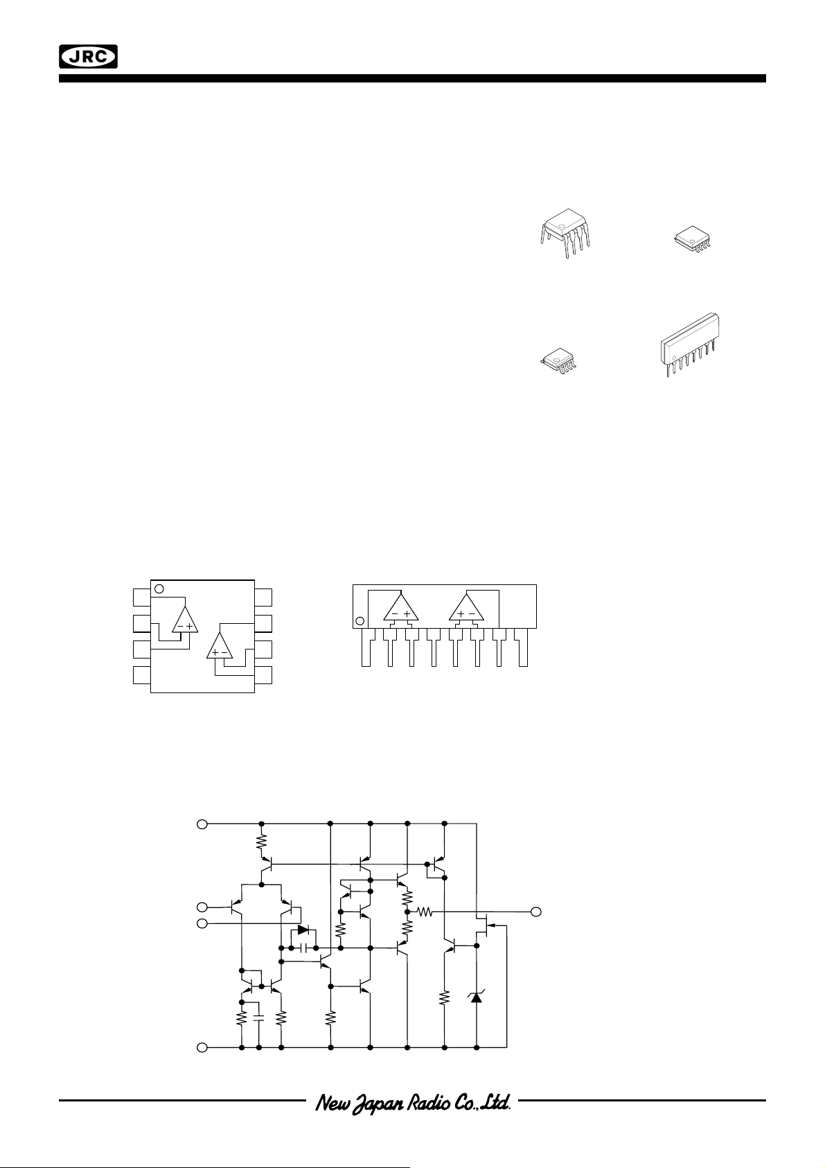
■ PIN CONFIGURATION
1
2
3
4
( Top View )
A
B
8
7
6
5
A B
1 234567 8
NJM4560D, NJM4560M, NJM4560E
NJM4560L
■ EQUIVALENT CIRCUIT ( 1/2 Shown )
V
+
- INPUT
+ INPUT
V
-
NJM4560D
( DIP8)
NJM4560E
( SOP8 )
OUTPUT
PIN FUNCTION
1. A OUTPUT
2. A - INPUT
3. A +INPUT
-
4. V
5. B +INPUT
6. B - INPUT
7. B OUTPUT
+
8. V
NJM4560
NJM4560M
( DMP8 )
NJM4560L
( SIP8 )
Ver.2011-12-12
-
-
Page 2

NJM4560
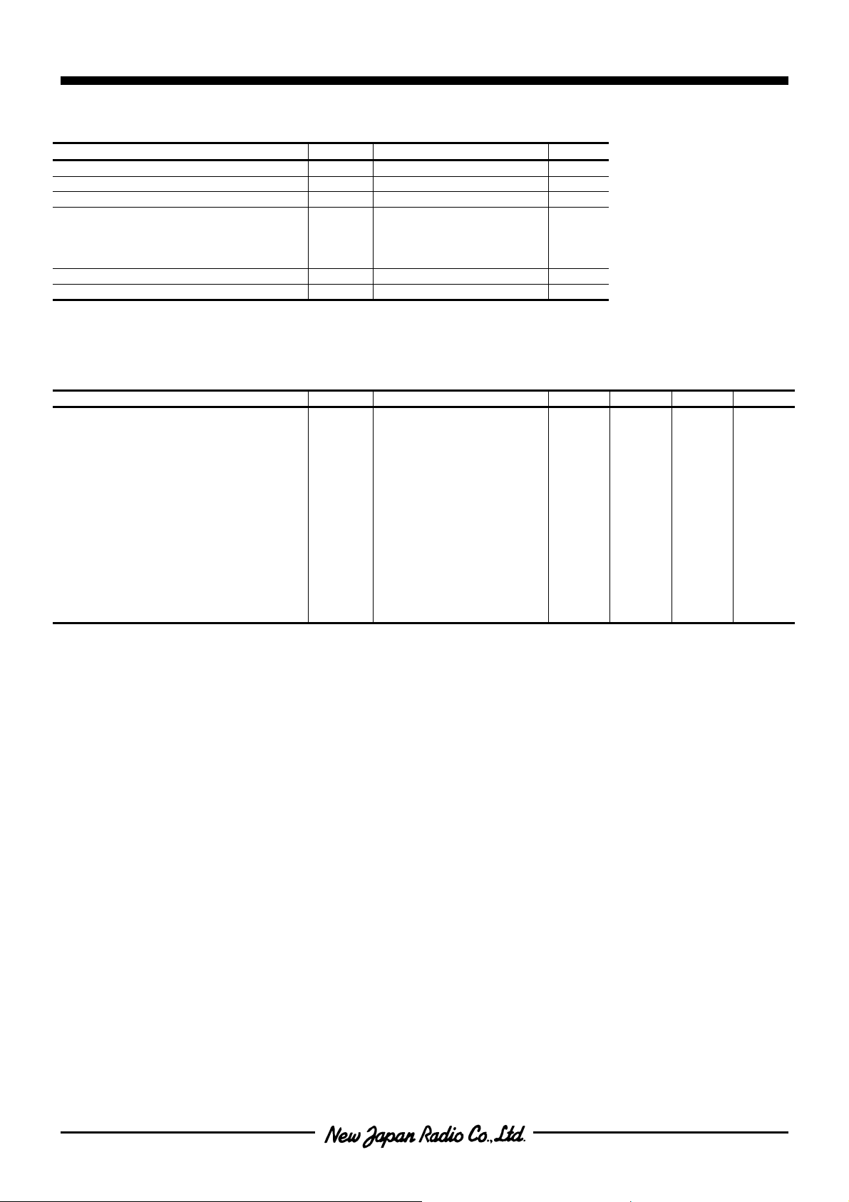
■ ABSOLUTE MAXIMUM RATINGS
( Ta=25˚C )
PARAMETER SYMBOL RATINGS UNIT
Supply Voltage V+/V- ± 18 V
Differential Input Voltage VD ± 30 V
Input Voltage VIC ± 15 ( note ) V
( DIP8 ) 500
Power Dissipation PD
Operating Temperature Range T
Storage Temperature Range T
( note ) For supply voltage less than ±15V,the absolute maximum input voltage is equal to the supply voltage.
-40~+85 ˚C
opr
-40~+125 ˚C
stg
■ ELECTRICAL CHARACTERISTICS
PARAMETER SYMBOL TEST CONDITION MIN. TYP. MAX. UNIT
Input Offset Voltage VIO
Input Offset Current IIO - 5 200 nA
Input Bias Current IB - 40 500 nA
Input Resistance RIN 0.3 5 - MΩ
Large Signal Voltage Gain AV R
Maximum Output Voltage Swing 1 V
Maximum Output Voltage Swing 2 V
Input Common Mode Voltage Range V
R
OM1
I
OM2
± 12 ± 14 - V
ICM
Common Mode Rejection Ratio CMR
Supply Voltage Rejection Ratio SVR
Operating Current ICC - 4.3 5.7 mA
Slew Rate SR - 4 - V/μs
Gain Bandwidth Product GB - 10 - MHz
Equivalent Input Noise Voltage VNI RIAA,RS=2kΩ,30kHz LPF - 1.2 - μVrms
( DMP8 ) 300
( SOP8 ) 300
mW
( SIP8 ) 800
( Ta=25˚C,V
≤10kΩ
R
S
≥2kΩ,VO=±10V 86 100 - dB
L
≥2kΩ ± 12 ± 14 - V
L
=25mA ± 10 ± 11.5 - V
O
≤10kΩ
R
S
≤10kΩ
R
S
- 0.5 6 mV
70 90 - dB
76.5 90 - dB
+/V-
=±15V )
-
-
Ver.2011-12-12
Page 3

■ TYPICAL CHARACTERISTICS
NJM4560
Ver.2011-12-12
-
-
Page 4

NJM4560
■ TYPICAL CHARACTERISTICS
[CAUTION]
The specifications on this databook are only
given for informat on , without any guarantee
as regards either mistakes or omiss ons. The
application circuits in this databook are
described only to show representative usages
of the product and not intended f or the
guarantee or permission of any r ght including
the industrial rights.
-
-
Ver.2011-12-12
Page 5

Mouser Electronics
Authorized Distributor
Click to View Pricing, Inventory, Delivery & Lifecycle Information:
NJR:
NJM4560MD NJM4560M NJM4560MD-TE1 NJM4560D NJM4560L NJM4560MD-TE2 NJM4560E NJM4560M-
TE1 NJM4560M-TE3 NJM4560M-TE2 NJM4560DD NJM4560E-TE1 NJM4560E-TE2
 Loading...