

Philips CBTU0808 Technical data

查询CBTU0808EE/G供应商
CBTU0808
Dual lane PCI Express port multiplexer
Rev. 01 — 2 June 2006 Product data sheet
1. General description
The CBTU0808 is a dual lane port multiplexer designed to provideconvenient and reliable
path switching for PCI Express signals. It is organized as two PCI Express lanes, each
consisting of a Transmit and Receivechannel.Each channel has four ports, two (A and B)
on the source (or host) side and two (A and B) on the destination (or device) side. Each
port provides a pair of signal lines to support PCIe differential signaling.
Using specially designed high-bandwidth and high off-isolation switch elements, source
and destination ports can be connected or isolated in three possible configurations:
source A and B to destinations A and B respectively; or source A to destination B
(remaining ports isolated), or all ports isolated.
2. Features
The switch elements are controlled by internal control logic to set switch positions in
accordance with these three configurations, selectable by CMOS inputs CTRL0 and
CTRL1 for lanes 0 and 1 respectively. Within a lane, the switch configuration is always
applied identically to both transmit and receive channels.
The CBTU0808 is packaged in a 48-ball, depopulated 9 × 9 grid, 0.5 mm ball pitch, thin
profile fine-pitch ball grid array (TFBGA) package, which (while requiring a minimum
5mm× 5 mm of board space) allows for adequate signal routing and escape using
conventional board technology.
n 2-lane wide PCI Express port multiplexer
n One transmit and one receive differential channel per lane
n Four ports per channel
n PCI Express signaling compliant
n High bandwidth: > 1 GHz
n Low OFF-feedthrough of < −35 dB at 1.25 GHz
n Low channel crosstalk of < −35 dB at 1.25 GHz
n Designed to match characteristic impedance of PCIe signaling environment
n Single 1.8 V supply operation
n ESD resilience of 2 kV HBM
n Available in 48-ball, 5 mm × 5 mm, 0.5 mm ball pitch TFBGA package, Pb-free/Green
3. Applications
n High-performance computing applications
n Port switching and docking applications
Philips Semiconductors
4. Ordering information
Table 1. Ordering information
Type number Solder process Package
Name Description Version
CBTU0808EE/G Pb-free (SnAgCu solder ball
TFBGA48 plastic thin fine-pitch ball grid array package;
compound)
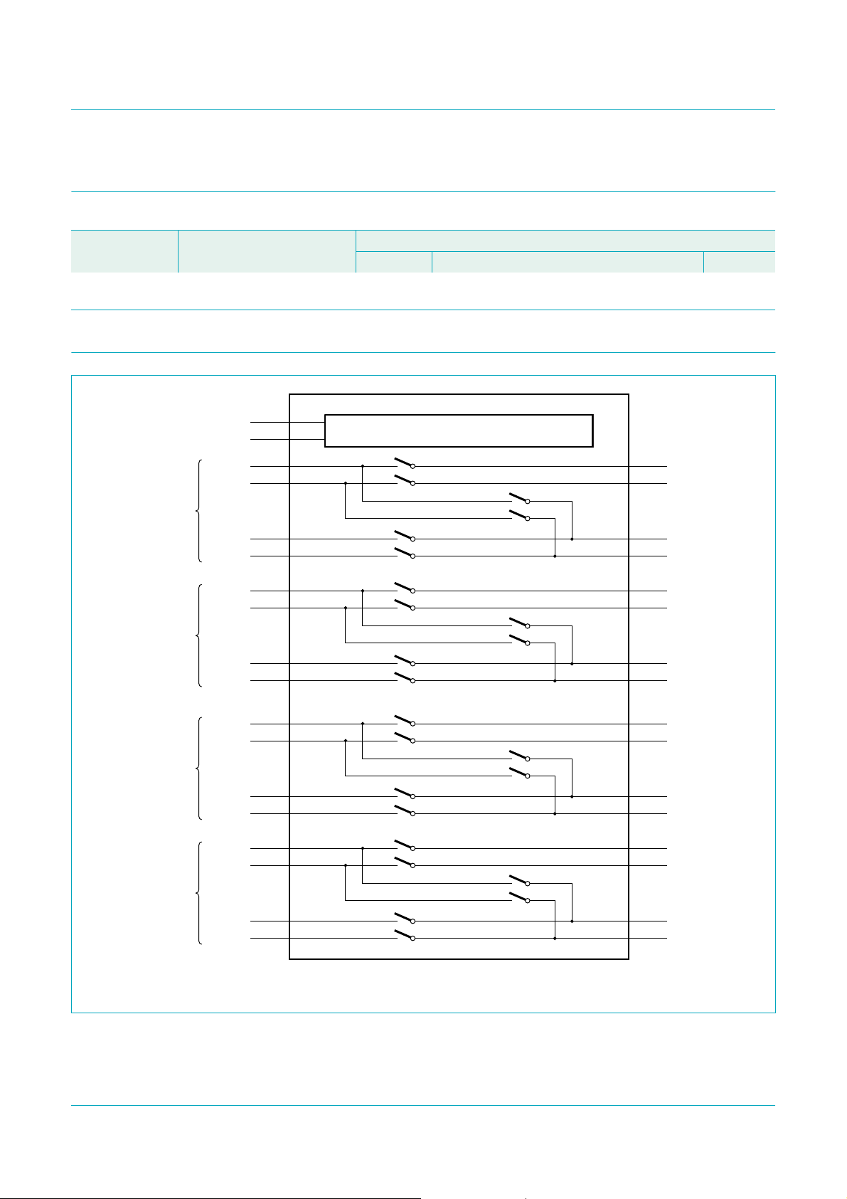
5. Functional diagram
CBTU0808
CTRL[1:0]
TEST[1:0]
CONTROL AND CONFIGURATION
CBTU0808
Dual lane PCI Express port multiplexer
SOT918-1
48 balls; body 5 × 5 × 0.8 mm
channel Tx0
channel Rx0
channel Tx1
TXSA0P
TXSA0N
TXSB0P
TXSB0N
RXSA0P
RXSA0N
RXSB0P
RXSB0N
TXSA1P
TXSA1N
TXSB1P
TXSB1N
RXSA1P
RXSA1N
TXDA0P
TXDA0N
TXDB0P
TXDB0N
LANE 0
RXDA0P
RXDA0N
RXDB0P
RXDB0N
TXDA1P
TXDA1N
TXDB1P
TXDB1N
LANE 1
RXDA1P
RXDA1N
channel Rx1
RXSB1P
RXSB1N
RXDB1P
RXDB1N
002aac139
Fig 1. Functional diagram
CBTU0808_1 © Koninklijke Philips Electronics N.V. 2006. All rights reserved.
Product data sheet Rev. 01 — 2 June 2006 2 of 16
Philips Semiconductors
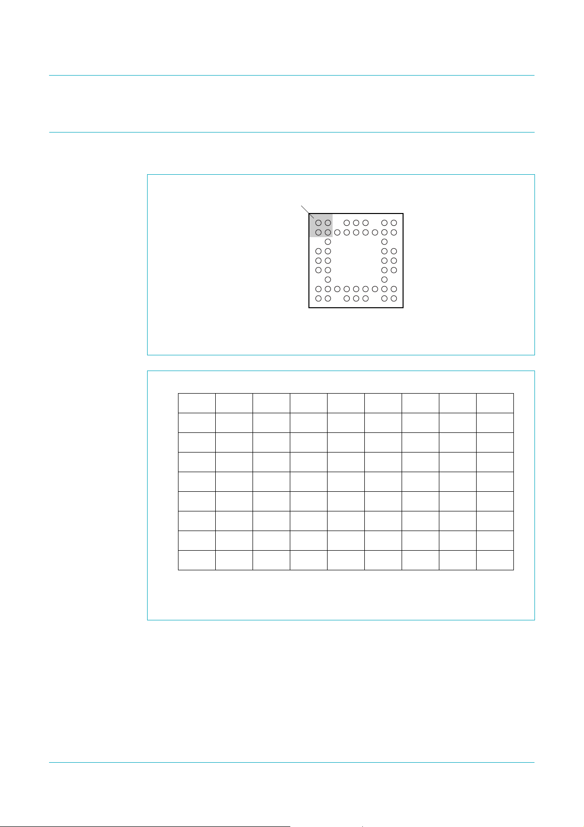
6. Pinning information
6.1 Pinning
CBTU0808
Dual lane PCI Express port multiplexer
ball A1
index area
A
B
C
D
E
F
G
H
J
Fig 2. Pin configuration for TFBGA48
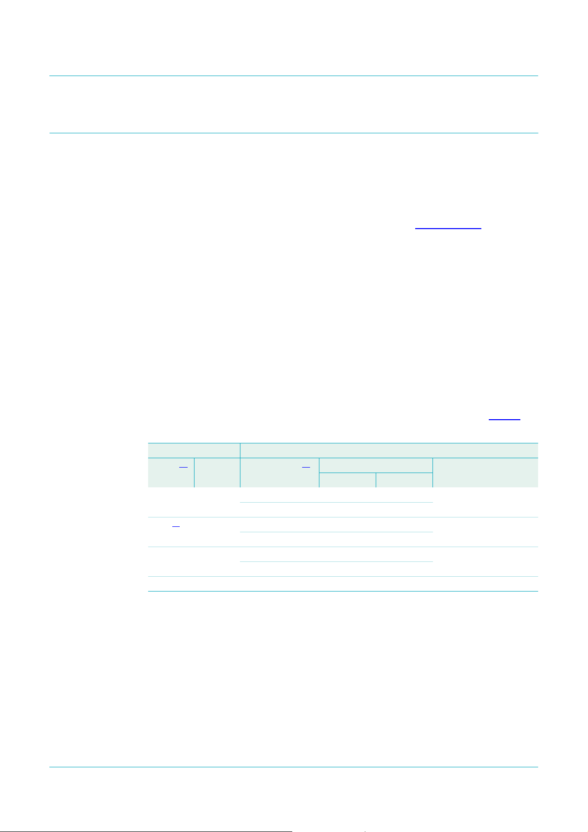
A
B
C
D
1
CTRL0
RXSA0P
RXSB0P
23456789
TXSB0P TXSA0P GND TXDA0P TXDB0P TEST1
GND TXSB0N TXSA0N V
RXSA0N RXDA0N
RXSB0N RXDB0N RXDB0P
CBTU0808EE/G
246891357
002aac213
Transparent top view
TXDA0N TXDB0N GND RXDA0P
DD
E
F
G
H
J
GND
TXSA1P
TXSB1P
TEST0
V
DD
TXSA1N TXDA1N TXDA1P
TXSB1N TXDB1N
GND RXSA1N RXSB1N V
RXSA1P RXSB1P GND RXDB1P RXDA1P CTRL1
RXDB1N RXDA1N GND TXDB1P
DD
V
DD
GND
002aac212
48-ball, 9 × 9 grid; top view. An empty cell indicates no ball is populated at that grid point.
Fig 3. Ball mapping
CBTU0808_1 © Koninklijke Philips Electronics N.V. 2006. All rights reserved.
Product data sheet Rev. 01 — 2 June 2006 3 of 16

Philips Semiconductors
6.2 Pin description
Table 2. Pin description
Signal group Symbol Pin Type Description
Test and
control
Signal ports TXSA0P, TXSA0N,
Power V
CBTU0808
Dual lane PCI Express port multiplexer
CTRL0 A1 CMOS
CTRL1 J9
TEST0 J1 CMOS
TEST1 A9 output Test output. Used for test purposes only.
A4, B4,
TXSB0P, TXSB0N
RXSA0P, RXSA0N,
RXSB0P, RXSB0N
TXSA1P, TXSA1N,
TXSB1P, TXSB1N
RXSA1P, RXSA1N,
RXSB1P, RXSB1N
TXDA0P, TXDA0N,
TXDB0P, TXDB0N
RXDA0P, RXDA0N,
RXDB0P, RXDB0N
TXDA1P, TXDA1N,
TXDB1P, TXDB1N
RXDA1P, RXDA1N,
RXDB1P, RXDB1N
DD
GND A5, B2,
A2, B3
B1, C2,
D1, D2
F1, F2,
H1, G2
J2, H3,
J4, H4
A6, B6,
A8, B7
B9, C8,
D9, D8
F9, F8,
H9, G8
J8, H7,
J6, H6
B5, E2,
E8, H5
B8, E1,
E9, H2,
H8, J5
input
input
signal
port
signal
port
signal
port
signal
port
signal
port
signal
port
signal
port
signal
port
power power supply pins
power ground pins
Switch configuration control inputs. See
Table 3 “Switch configuration truth table”.
Test input. Used for test purposes only.
Should beleftopen-circuit during normal
operation. An internal pull-down resistor
will default this pin to a LOW state.
Should be left open-circuit in normal
application.
Transmit ports A and B differential signal
terminals for Lane 0, Source side.
Receive ports A and B differential signal
terminals for Lane 0, Source side.
Transmit ports A and B differential signal
terminals for Lane 1, Source side.
Receive ports A and B differential signal
terminals for Lane 1, Source side.
Transmit ports A and B differential signal
terminals for Lane 0, Destination side.
Receive ports A and B differential signal
terminals for Lane 0, Destination side.
Transmit ports A and B differential signal
terminals for Lane 1, Destination side.
Receive ports A and B differential signal
terminals for Lane 1, Destination side.
CBTU0808_1 © Koninklijke Philips Electronics N.V. 2006. All rights reserved.
Product data sheet Rev. 01 — 2 June 2006 4 of 16
Philips Semiconductors
7. Functional description
7.1 Functional description
7.1.1 General information
The CBTU0808 Dual lane PCI Express port multiplexeris designed to allow port switching
of up to two PCI Express lanes (each including a Transmit and Receive channel)
according to three switch configuration settings (described in Section 7.1.2.1). The basic
switch element of the CBTU0808 is designed integrally with its package and chip
interconnect to present an optimum characteristic on-impedance when used in a
PCI Express signaling environment, and to provide high off-port isolation and low
crosstalk.
7.1.2 Functional information
The following paragraphs describe the control and configuration possibilities available in
the CBTU0808.
7.1.2.1 Switch configuration
The position of the port switches is controlled by CMOS input signals CTRL[1:0] and can
be overridden by CMOS input TEST0 to disconnect (open) all ports between source and
destination. For a given lane, the switch positions are always identical between transmit
and receive channels. Lane 0 is controlled by CTRL0 and Lane 1 is controlled by CTRL1.
The truth table for the switch position as a function of these inputs is shown in Table 3.
CBTU0808
Dual lane PCI Express port multiplexer
Table 3. Switch configuration truth table
Inputs Function
[1]
CTRLn
LOW LOW An R
HIGH
LOW HIGH An high-Z high-Z All ports open-circuit
> LOW HIGH Test mode for internal use only do not use
[1] n is the Lane number (0 or 1).
[2] CTRL1 or CTRL0 = HIGH.
TEST0 Source ports
Bn high-Z R
[2]
LOW An high-Z R
Bn high-Z high-Z
Bn high-Z high-Z
[1]
Destination ports Comment
A B
on
high-Z SA:DA/SB:DB
on
on
(Dual Through mode)
SA:DB
(Single Cross mode)
(Disconnect mode)
CBTU0808_1 © Koninklijke Philips Electronics N.V. 2006. All rights reserved.
Product data sheet Rev. 01 — 2 June 2006 5 of 16
 Loading...