

Philips CBTS3253 Technical data

查询CBTS3253供应商查询CBTS3253供应商
INTEGRATED CIRCUITS
CBTS3253
Dual 1-of-4 FET multiplexer/demultiplexer
with Schottky diode clamping
Product data 2002 Nov 06
Philips
Semiconductors
Philips Semiconductors Product data
CBTS3253
Dual 1-of-4 FET multiplexer/demultiplexer
with Schottky diode clamping
2
2002 Nov 06
FEATURES
•5 Ω switch connection between two ports
•TTL-compatible input levels
•Schottky diodes on I/O clamp undershoot
•Minimal propagation delay through the switch
•ESD protection exceeds 2000 V HBM per JESD22-A114,
200 V MM per JESD22-A115 and 1000 V CDM per JESD22-C101
•Latch-up testing is done to JESDEC Standard JESD78 which
exceeds 100 mA
DESCRIPTION
The CBTS3253 is a dual 1-of-4 high-speed TTL-compatible FET
multiplexer/demultiplexer. The low on resistance of the switch allows
inputs to be connected to outputs without adding propagation delay
or generating additional ground bounce noise.
1OE
, 2OE, S0, and S1 select the appropriate B output for the
A-input data.
Internal Schottky diode provides I/O undershoot protection
The CBTS3253 is characterized for operation from –40 to +85°C.
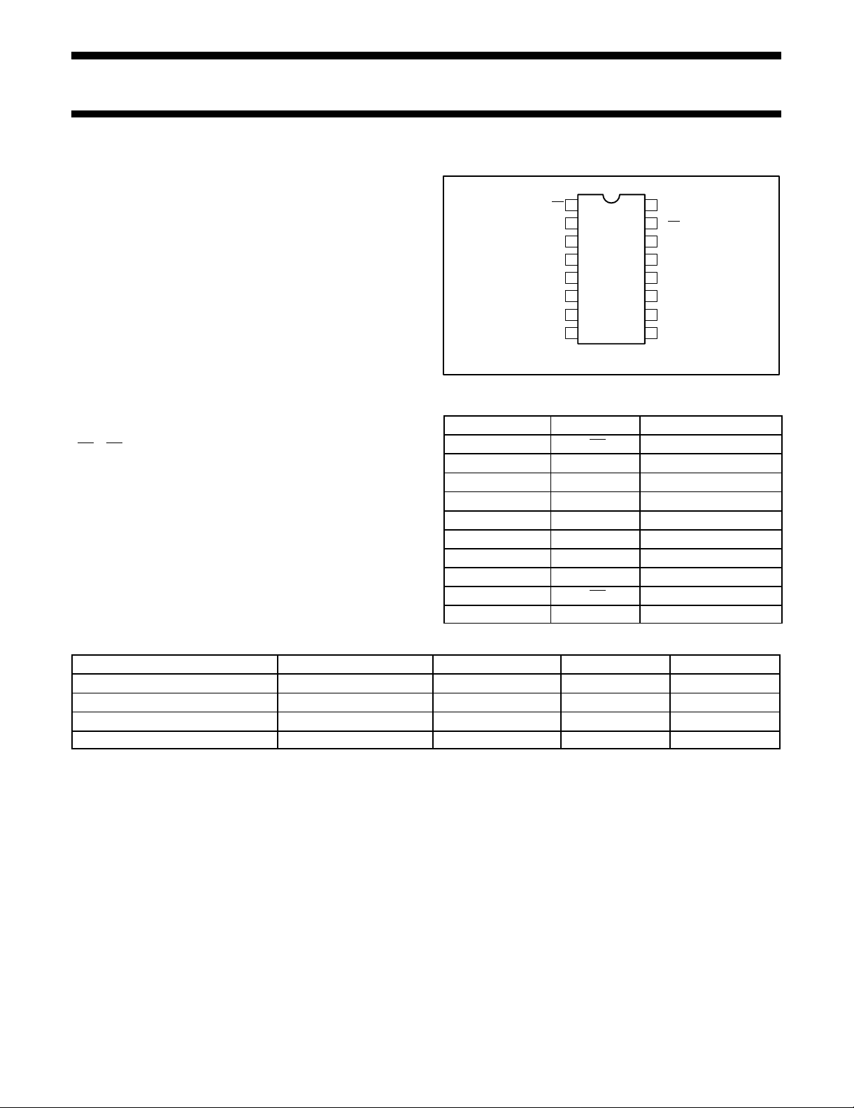
PIN CONFIGURATION
1
2
3
4
5
6
7
89
10
11
12
13
14
15
16
1B4
1B3
1B2
1B1
1A
1OE
GND
V
CC
S0
SA00574
S1
2OE
2B4
2B3
2B2
2B1
2A
PIN DESCRIPTION
PIN NUMBER SYMBOL NAME AND FUNCTION
1 1OE Output enable
2 S1 Select-control input
3, 4, 5, 6 1B[1–4] B outputs
7 1A A input
8 GND Ground (0 V)
9 2A A input
10, 11, 12, 13 2B[1–4] Select-control input
14 S0 Select-control input
15 2OE Output enable
16 V
CC
Positive supply voltage
ORDERING INFORMATION
PACKAGES TEMPERATURE RANGE ORDER CODE TOPSIDE MARK DWG NUMBER
16-pin plastic SO –40 to 85 °C CBTS3253D CBTS3257 SOT109-1
16-pin plastic SSOP –40 to 85 °C CBTS3253DB CS3253 SOT338-1
16-pin plastic SSOP (QSOP) –40 to 85 °C CBTS3253DS CBS3253 SOT519-1
16-pin plastic TSSOP –40 to 85 °C CBTS3253PW CBS3253 SOT403-1
Standard packing quantities and other packaging data is available at www.philipslogic.com/packaging.
Philips Semiconductors Product data
CBTS3253
Dual 1-of-4 FET multiplexer/demultiplexer
with Schottky diode clamping
2002 Nov 06
3
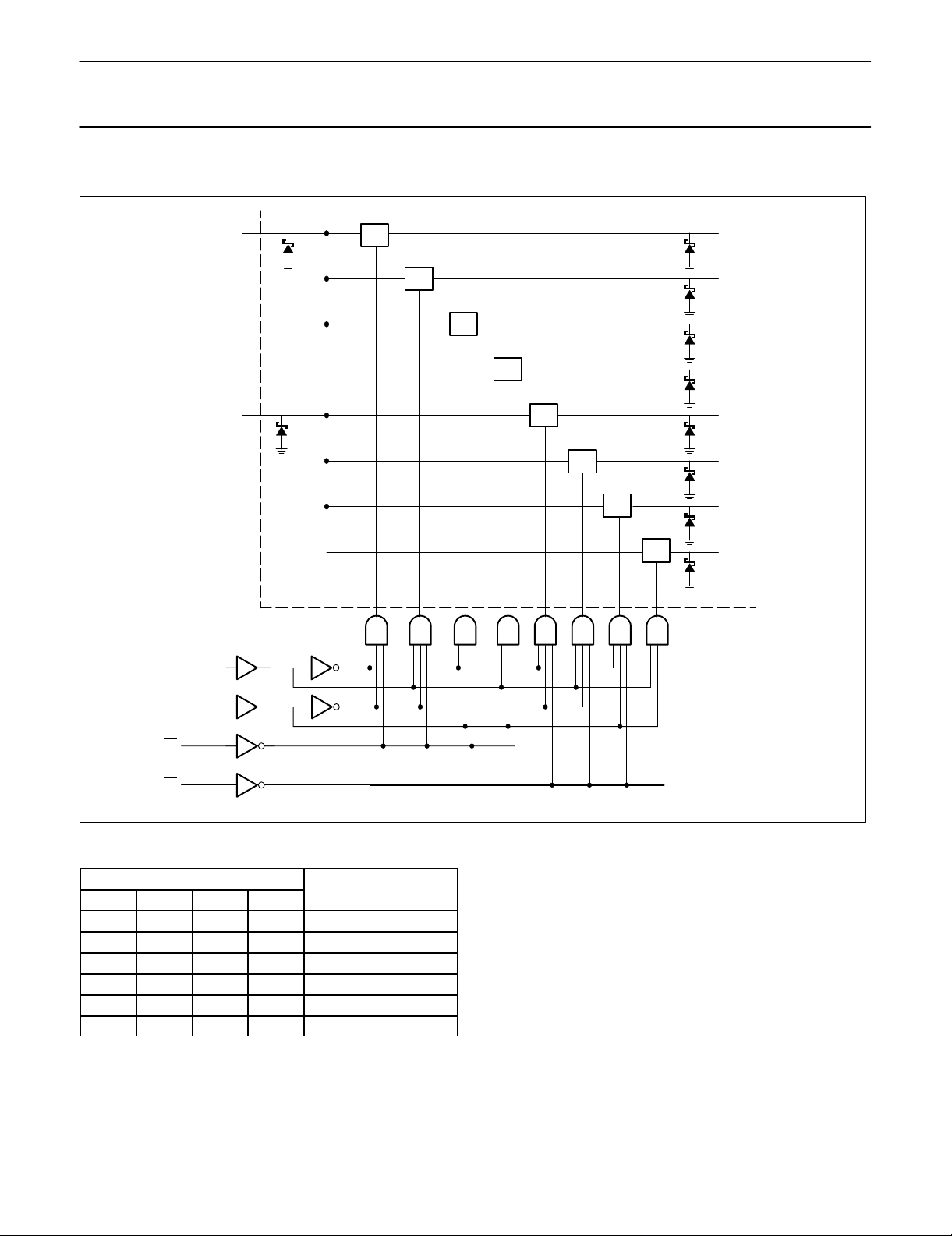
LOGIC DIAGRAM (positive logic)
SA00637
1A
1B1
1B2
1B3
1B4
2B1
2B2
2B3
2B4
SW
SW
SW
SW
SW
SW
SW
SW
2A
7
S0
S1
1OE
2OE
9
14
2
1
15
6
5
4
3
10
11
12
13
FUNCTION TABLE
INPUTS
OE1 OE2 S1 S0
FUNCTION
H X X X Disconnect 1A
X H X X Disconnect 2A
L L L L 1A to 1B1 and 2A to 2B1
L L L H 1A to 1B2 and 2A to 2B2
L L H L 1A to 1B3 and 2A to 2B3
L L H H 1A to 1B4 and 2A to 2B4
Philips Semiconductors Product data
CBTS3253
Dual 1-of-4 FET multiplexer/demultiplexer
with Schottky diode clamping
2002 Nov 06
4
ABSOLUTE MAXIMUM RATINGS
1
SYMBOL
PARAMETER CONDITIONS RATING UNIT
V
CC
DC supply voltage –0.5 to +7.0 V
V
I
DC input voltage
2
–0.5 to +7.0 V
Continuous channel current 128 mA
I
K
Input clamp current V
I/O
< 0 –50 mA
T
stg
Storage temperature range –65 to +150 °C
NOTES:
1. Stresses beyond those listed may cause permanent damage to the device. These are stress ratings only and functional operation of the
device at these or any other conditions beyond those indicated under “recommended operating conditions” is not implied. Exposure to
absolute-maximum-rated conditions for extended periods may affect device reliability.
2. The input and output negative-voltage ratings may be exceeded if the input and output clamp-current ratings are observed.
3. The package thermal impedance is calculated in accordance with JESD 51-7.
RECOMMENDED OPERATING CONDITIONS
LIMITS
SYMBOL PARAMETER
MIN MAX
UNIT
V
CC
DC supply voltage 4.5 5.5 V
V
IH
High-level input voltage 2 — V
V
IL
Low-level Input voltage — 0.8 V
T
amb
Operating free-air temperature range –40 +85 °C
NOTE:
1. All unused control inputs of the device must be held at V
CC
or GND to ensure proper device operation.
DC ELECTRICAL CHARACTERISTICS
LIMITS
SYMBOL PARAMETER TEST CONDITIONS T
amb
= –40 to +85 °C UNIT
MIN TYP
1
MAX
A or B inputs — — –0.8
V
IK
Input clamp voltage
Control inputs
VCC = 4.5 V; II = –18 mA
— — –1.2
V
V
P
Pass voltage VI = VCC = 5.5 V; I/O = –100 µA 3.4 3.6 3.9 V
I
I
Input leakage current VCC = 5.5 V; VI = 5.5 or GND — — ±1 µA
I
CC
Quiescent supply current VCC = 5.5 V; IO = 0, VI = VCC or GND — — 3 µA
∆I
CC
Control inputs
2
VCC = 5.5 V, one input at 3.4 V,
other inputs at V
CC
or GND
— — 2.5 mA
C
I
Control pins VI= 3 V or 0 — 4.5 — pF
Power-off leakage
A port VO = 3 V or 0; OE = V
CC
— 24.6 —
C
IO(OFF)
Power-off leakage
current
B port VO = 3 V or 0; OE = V
CC
— 7.6 —
pF
VI = 0 V; II = 64 mA — 5 7
r
on
3
On-resistance VCC = 4.5 V
VI = 0 V; II = 30 mA — 5 7
Ω
on CC
VI = 2.4 V; II = –15 mA — 10 15
NOTES:
1. All typical values are at V
CC
= 5 V, T
amb
= 25 °C.
2. This is the increase in supply current for each input that is at the specified TTL voltage level rather than VCC or GND
3. Measured by the voltage drop between the A and the B terminals at the indicated current through the switch.
On-state resistance is determined by the lowest voltage of the two (A or B) terminals.
 Loading...