

Philips CBT6832E Technical data
查询CBT6832E供应商查询CBT6832E供应商
INTEGRATED CIRCUITS
CBT6832E
16-bit controlled enable rate
1-of-2 multiplexer/demultiplexer with
precharged outputs and Schottky
undershoot protection for live insertion
Product specification
Supersedes data of 2000 May 19
2000 Sep 01
Philips Semiconductors Product specification
16-bit controlled enable rate 1-of-2 multiplexer/demultiplexer with precharged
outputs and Schottky undershoot protection for live insertion
FEA TURES
•5 Ω typical r
on
•Pull-up on B port
•Undershoot protection on A port only: –2.0 V
•Near zero propagation delay
•Controlled enable rate
•V
operating range: +4.5 V to +5.5 V
CC
•> 100 MHz bandwidth (or clock rate) at 20 pF load capacitance
•56-pin TSSOP package
•Bias voltage pre-charges the B output when the channel is
disabled
•Latch-up protection exceeds 100 mA per JESD78
•ESD protection exceeds 2000 V HBM per JESD22-A114,
200 V MM per JESD22-A115 and 1000 V CDM per JESD22-C101
APPLICATION
•Provides PCI hot-plugging
DESCRIPTION
The CBT6832E is a 16-bit controlled enable rate 1-of-2
multiplexer/demultiplexer with precharged outputs and Schottky
undershoot protection for live insertion. Advantages of the CBT6832
include a propagation delay of 250 ps, resulting from 5 Ω channel
resistance, and low I/O capacitance. A port demultiplexes to either
1B and 2B, or to both. The switch is bi-directional.
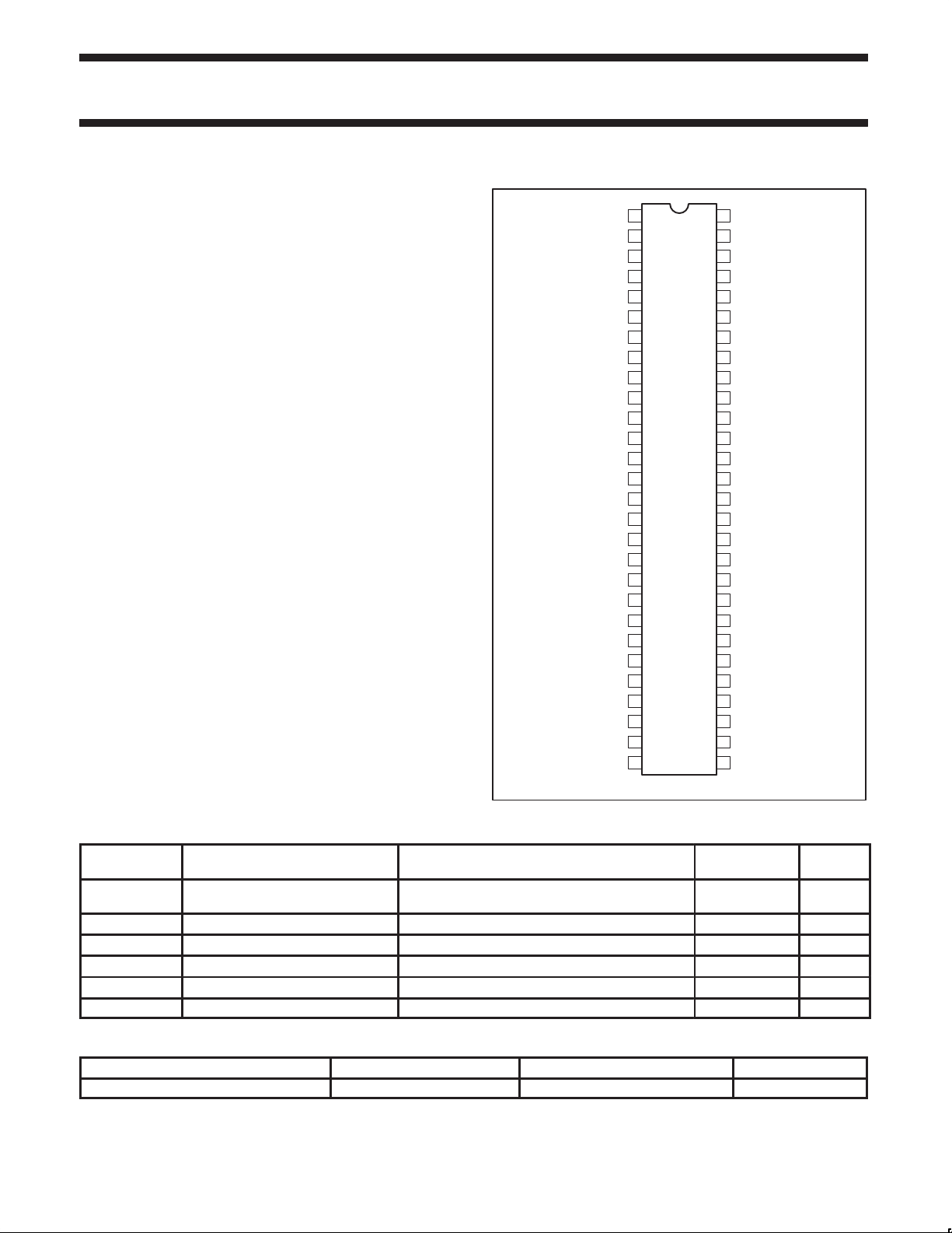
PIN CONFIGURATION
1
2B1
2
3
2A
4
3B1
5
4B1
6
4A
7
5B1
8
6B1
9
6A
10
7B1
11
8B1
12 45
13
14
V
CC
15
9B1
16
10B1
17
10A
18 39
11B1
19 38
12B1
20
21
13B1
22
14B1
23
14A
24
15B1
25 32
26 31 16B216A
27 30 V
V
BIAS1
28 29SEL1 SEL2
CBT6832E
1A
561B1
1B2
55
2B2
54
3A
53
3B2
52
4B2
51
5A
50
5B2
49
6B2
48
7A
47
7B2
46
8B28A
GND
44GND
V
43
CC
42
9A
9B2
41
40
10B2
11A
11B2
12B2
3712A
36
13A
35
13B2
34
14B2
33
15A
15B216B1
BIAS2
SW00478
QUICK REFERENCE DA TA
SYMBOL PARAMETER
C
C
C
C
t
PLH
t
PHL
C
IN
OFF B
OFF A
ON 1
ON 2
Propagation delay
An to Bn or Bn to An
Input capacitance control pins VI = 0 V or V
B capacitance, switch off Outputs disabled; VO = 0 V 8 pF
A capacitance, switch off Outputs disabled; VO = 0 V 13 pF
One channel enabled capacitance One B enabled; VO = 0 V 21 pF
Both channels enabled capacitance Both B channels enabled; VO = 0 V 34 pF
CL = 50 pF; VCC = 5 V .25 ns
CONDITIONS
T
= 25°C; GND = 0 V
amb
CC
TYPICAL UNIT
4.5 pF
ORDERING INFORMATION
PACKAGES TEMPERATURE RANGE ORDER CODE DWG NUMBER
56-Pin Plastic TSSOP Type II 0°C to +70°C CBT6832E DGG SOT364-1
2000 Sep 01 853-2217 24481
2
Philips Semiconductors Product specification
SYMBOL
PARAMETER
UNIT
16-bit controlled enable rate 1-of-2 multiplexer/demultiplexer with precharged
outputs and Schottky undershoot protection for live insertion
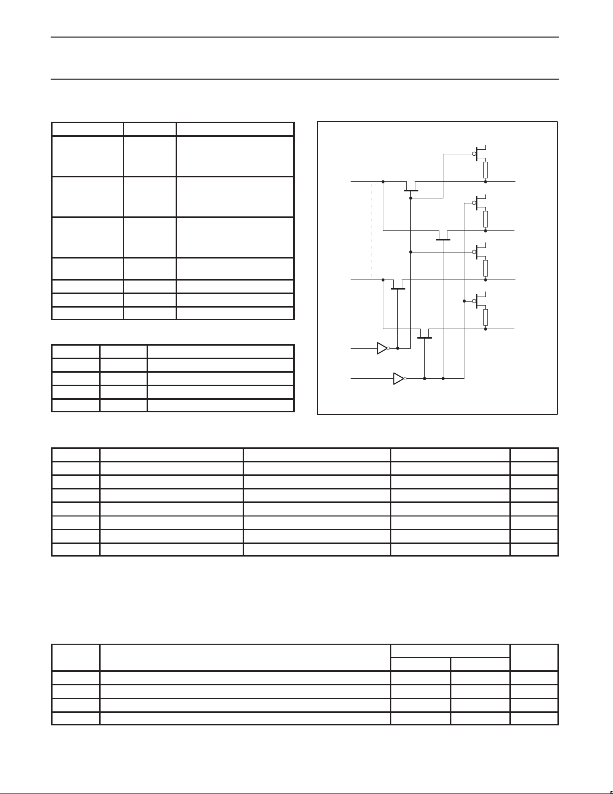
PIN DESCRIPTION
PIN NUMBER SYMBOL NAME AND FUNCTION
3, 6, 9, 12, 17,
20, 23, 26, 33,
36, 39, 42, 47,
1A1–16A1 Inputs
50, 53, 56
1, 2, 4, 5, 7, 8,
10, 11, 15, 16,
18, 19, 21, 22,
1B1–16B1 Outputs
24, 25
31, 32, 34, 35,
37, 38, 40, 41,
45, 46, 48, 49,
1B2–16B2 Outputs
51, 52, 54, 55
V
,
27, 30
BIAS1
V
BIAS2
Precharge bias voltage inputs
28, 29 SEL1, SEL2 Select-control inputs
13, 44 GND Ground (0 V)
14, 43 V
CC
Positive supply voltage
FUNCTION TABLE
SEL1 SEL2 FUNCTION
L H nA to nB1
H L nA to nB2
L L nA to nB1 and nB2
H H nB1, nB2 = V
BIAS
LOGIC DIAGRAM
1A
16A
SEL1
SEL2
CBT6832E
V
BIAS1
PULLUP
V
V
V
BIAS2
PULLUP
BIAS1
PULLUP
BIAS2
PULLUP
1B1
1B2
16B1
16B2
SV01801
ABSOLUTE MAXIMUM RA TINGS
SYMBOL
V
CC
I
IK
V
I
V
OUT
I
OUT
T
stg
Θ
JA
DC supply voltage –0.5 to +7.0 V
DC input diode current VI < 0 –50 mA
DC input voltage
DC output voltage
DC output current output in Low state 120 mA
Storage temperature range –65 to +150 °C
Power dissipation 95 °C/W
PARAMETER CONDITIONS RATING UNIT
3
3
1, 2
–0.5 to +7.0 V
output in Off or High state –0.5 to +7.0 V
NOTES:
1. Stresses beyond those listed may cause permanent damage to the device. These are stress ratings only and functional operation of the
device at these or any other conditions beyond those indicated under “recommended operating conditions” is not implied. Exposure to
absolute-maximum-rated conditions for extended periods may affect device reliability .
2. The performance capability of a high-performance integrated circuit in conjunction with its thermal environment can create junction
temperatures which are detrimental to reliability. The maximum junction temperature of this integrated circuit should not exceed 150°C.
3. The input and output voltage ratings may be exceeded if the input and output current ratings are observed.
RECOMMENDED OPERATING CONDITIONS
LIMITS
MIN MAX
V
T
CC
V
V
amb
DC supply voltage 4.5 5.5 V
High-level input voltage 2.0 V
IH
Low-level Input voltage 0.8 V
IL
Operating free-air temperature range 0 +70 °C
2000 Sep 01
3
 Loading...