

Philips CBT6820 Datasheet

INTEGRATED CIRCUITS
CBT6820
20-bit bus switch with precharged outputs
and Schottky undershoot protection for
live insertion
Product specification
1999 Apr 05
Philips Semiconductors Product specification
20-bit bus switch with precharged outputs and
Schottky undershoot protection for live insertion
FEA TURES
•TTL compatible inputs and outputs
•5Ω switch connection between two port A and port B
•Thin shrink small outline (TSSOP)
•Undershoot protection included to prevent shoot through level
changes
•Bias voltage pre-charges the outputs to minimize signal distortion
during live insertion
DESCRIPTION
The CBT6820 provides twenty bits of high-speed TTL-compatible
bus switching. The low on-state resistance of the switch allows
bi-directional connections to be made while adding near-zero
propagation delay. The device also precharges the B port to a
user-selectable bias voltage (BIASV) to minimize live-insertion
noise.
The device is organized as two 10-bit switch with individual enable
(OE) input. When OE is low, the switch is on and port A is
connected to port B. When OE is high, the switch between port A
and port B is open and the B port is precharged to BIASV through
the equivalent of a 10-kΩ resistor.
Special clamp circuitry and Schottky diode clamps to ground are
used to prevent an under voltage on the A side (Vin < GND) from
causing the B side precharge voltage to drop below the ‘‘1” state.
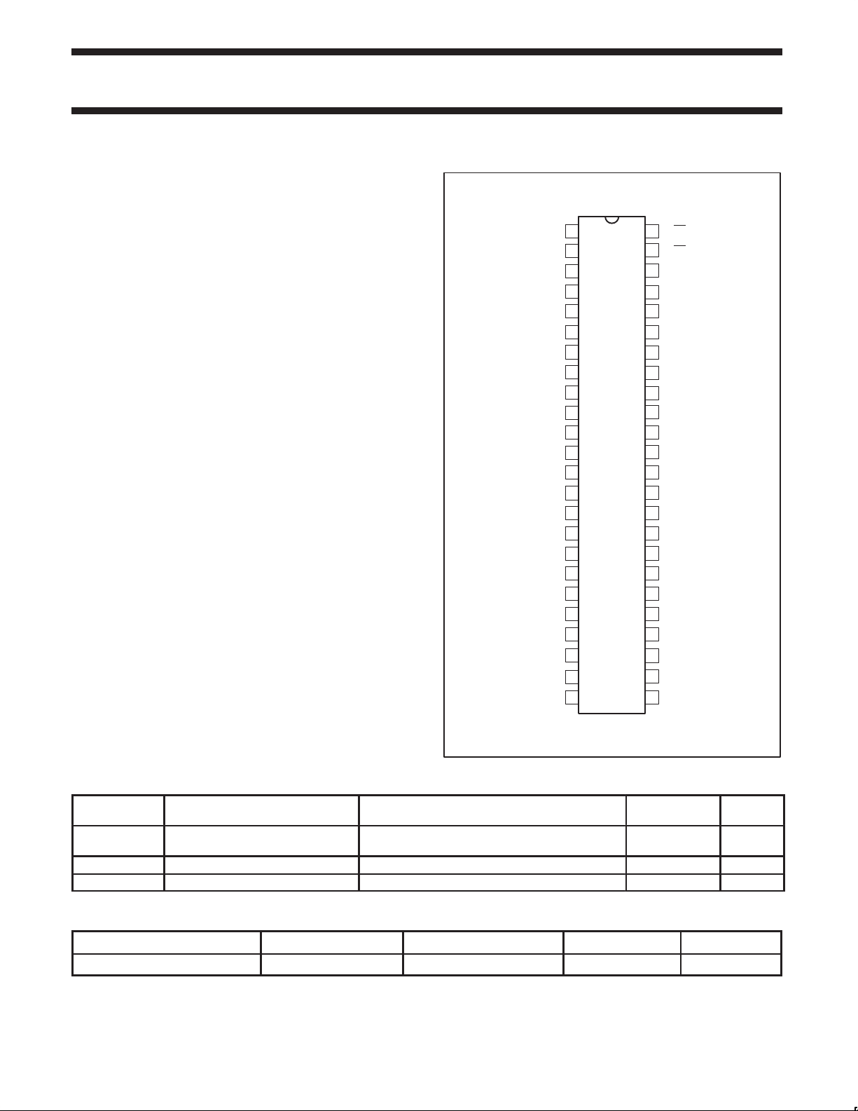
PIN CONFIGURATION
BIASV
1A1
1A2
1A3
1A4
1A5
1A6
GND
1A7
1A8
1A9
1A10
2A1
2A2
V
2A3
GND
2A4
2A5
2A6
2A7
2A8
2A9
2A10
CBT6820
1
2
3
4
5
6
7
8
9
10
11
12
13
14
15
CC
16
17
18
19
20
21
22
23
24
1OE
48
2OE
47
1B1
46
1B2
45
44
1B3
43
1B4
42
1B5
GND
41
40
1B6
39
1B7
1B8
38
1B9
37
1B10
36
2B1
35
2B2
34
2B3
33
GND
32
2B4
31
2B5
30
2B6
29
2B7
28
2B8
27
2B9
26
2B10
25
SA00520
QUICK REFERENCE DA TA
SYMBOL PARAMETER
t
PLH/tPHL
C
IN
C
I/O
Propagation delay
An to Bn or Bn to An
Input capacitance 4.5 pF
Input/output capacitance Outputs disabled; VO = 0 V or V
CL = 50 pF, VCC = 5 V 0.25 ns
CONDITIONS
T
= 25°C; GND = 0V
amb
CC
TYPICAL UNIT
9.5 pF
ORDERING INFORMATION
PACKAGES TEMPERATURE RANGE OUTSIDE NORTH AMERICA NORTH AMERICA DWG NUMBER
48-Pin Plastic TSSOP Type II –40°C to +85°C CBT6820 DGG CBT6820 DGG SOT362–1
1999 Apr 05 853–2152 21177
2
Philips Semiconductors Product specification
SYMBOL
PARAMETER
UNIT
20-bit bus switch with precharged outputs and
Schottky undershoot protection for live insertion
PIN DESCRIPTION
PIN NUMBER SYMBOL NAME AND FUNCTION
1 BIASV Bias voltage
2, 3, 4, 5, 6,
7, 9, 10, 11,12
1A1–1A10 Port 1A1 to Port 1A10
8, 17, 32, 41 GND Ground (V)
13, 14, 16, 18, 19,
20, 21, 22, 23, 24
15 V
35, 34, 33, 31, 30,
29, 28, 27, 26, 25
46, 45, 44, 43, 42,
40, 39, 38, 37, 36
2A1–2A10 Port 2A1 to Port 2A10
CC
Positive supply voltage
2B1–2B10 Port 2B1 to Port 2B10
1B1–1B10 Port 1B1 to Port 1B10
48, 47 1OE, 2OE Switch enables
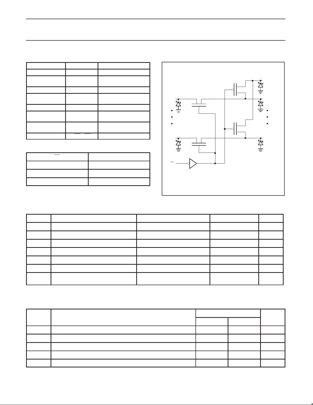
FUNCTION TABLE
OE STATE
L A Port = B Port
H A Port = Z
H B Port = BIASV
H = High voltage level
L = Low voltage level
Z = High impedance “off” state
LOGIC SYMBOL
xA10
2, 13
xA1
12, 24
48, 47
xOE
where x = 1 – 2
CBT6820
1
BIASV
46, 35
xB1
36, 25
xB10
SA00506
ABSOLUTE MAXIMUM RATINGS
SYMBOL PARAMETER CONDITIONS RATING UNIT
V
I
V
BIASV
T
øJA
I
V
SW
CC
IK
stg
DC supply voltage –0.5 to +7.0 V
DC clamp diode current VI < 0 –50 mA
DC input voltage
I
DC continuous channel current VO = 0 to V
1
CC
–0.5 to +7.0 V
±128 mA
DC bias voltage –0.5 to +7.0 V
Storage temperature range –65 to 150 °C
Plastic thin shrink small outline package
(TSSOP)
104 °C/W
NOTE:
1. The input and output voltage ratings may be exceeded if the input and output current ratings are observed.
RECOMMENDED OPERATING CONDITIONS
LIMITS
Min Max
V
CC
BIASV DC supply voltage 1.3 V
V
V
T
amb
DC supply voltage 4.0 5.5 V
High-level input voltage (control pin) 2.0 V
IH
Low-level Input voltage (control pin) 0.8 V
IL
Operating free-air temperature range –40 +85 °C
CC
V
1999 Apr 05
3
 Loading...