

Philips CBT3857 Datasheet

INTEGRATED CIRCUITS
CBT3857
10-bit bus switch with 10 kΩ pull-down
termination resistors
Product specification
Supersedes data of 1998 Dec 10
1999 Sep 14
Philips Semiconductors Product specification
10-bit bus switch with 10 kΩ pull-down
termination resistors
FEA TURES
•Enable signal is SSTL_2 compatible
•Optimized for use in Double Data Rate (DDR) SDRAM
applications
•Flow-through architecture optimizes PCB layout
•Designed to be used with 200 Mbps
•Switch on resistance is designed to eliminate the need for series
resistor to DDR SDRAM
•Internal 10 kΩ pull-down resistors on B port
•Internal 50 kΩ pull-up resistor on output enable input
•Full DDR solution provided when used with SSTL16857 and
PCK857
•Latch-up protection exceeds 500 mA per JESD78
•ESD protection exceeds 2000 V HBM per JESD22-A114,
200 V MM per JESD22-A115 and 1000 V CDM per JESD22-C101
QUICK REFERENCE DATA
SYMBOL PARAMETER
C
t
PLH
t
PHL
C
OUT
I
CCZ
IN
Propagation delay
An to Yn
CL = 30 pF; VCC = 3.3 V 720 ps
Input capacitance VI = 0 V or V
Output capacitance Outputs disabled; VO = 0 V or V
Total supply current VCC = 3.6 V 1 mA
CBT3857
DESCRIPTION
This 10-bit bus switch is designed for 3 V to 3.6 V VCC operation
and SSTL_2 output enable (OE
When OE is LOW, the 10-bit bus switch is on and port A is
connected to port B. When OE
high-impedance state exists between the two ports.
The low on-state resistance of the switch allows connections to be
made with minimal propagation delay.
The CBT3857 is characterized for operation from 0°C to +85°C.
CONDITIONS
T
= 25°C; GND = 0 V
amb
CC
CC
) input levels.
is HIGH, the switch is open, and a
TYPICAL UNIT
2.8 pF
6.4 pF
ORDERING INFORMATION
PACKAGES TEMPERATURE RANGE ORDER CODE DWG NUMBER
24-Pin Plastic TSSOP Type I 0°C to +85°C CBT3857 PW SOT355–1
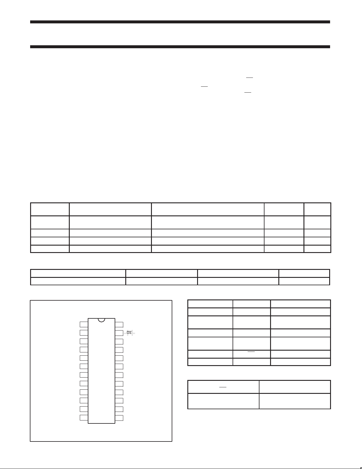
PIN CONFIGURATION
V
1
REF
2
A1
3
A2
4
A3
5
A4
6
A5
7
A6
8
A7
9
A8
10
A9
11
A10
12
GND
24
Vcc
OE
23
22
B1
21
B2
20
B3
19
B4
18
B5
17
B6
16
B7
15
B8
B9
14
13
B10
PIN DESCRIPTION
PIN NUMBER SYMBOL NAME AND FUNCTION
1 V
2, 3, 4, 5, 6,
7, 8, 9, 10, 11
REF
A1–A10 Inputs
Reference output voltage
12 GND Ground (V)
22, 21, 20, 19, 18,
17, 16, 15, 14, 13
B1–B10 Outputs
23 OE Output enable
24 V
CC
Positive supply voltage
FUNCTION TABLE
INPUT
OE
L A port = B port
H Disconnect
H = High voltage level
L = Low voltage level
FUNCTION
SA00516
1999 Sep 14 853–2168 22329
2

Philips Semiconductors Product specification
SYMBOL
PARAMETER
UNIT
10-bit bus switch with 10 kΩ pull-down
termination resistors
LOGIC DIAGRAM (POSITIVE LOGIC)
22
B1
R
INT
13
B10
R
INT
A10
V
OE
A1
REF
2
11
23
1
SW
SW
CBT3857
SIMPLIFIED SCHEMATIC, EACH FET SWITCH
BA
OE
SA00518
SA00517
ABSOLUTE MAXIMUM RA TINGS
SYMBOL
V
CC
I
IK
V
I
T
stg
V
I
DC supply voltage –0.5 to +4.6 V
DC input clamp current V
DC input voltage range (OE only)
Storage temperature range –65 to 150 °C
DC input voltage range (except OE)
PARAMETER CONDITIONS RATING UNIT
1, 3
< 0 –50 mA
2
2
I/O
VCC + 0.5 V
–0.5 to 4.6 V
NOTES:
1. Stresses beyond those listed may cause permanent damage to the device. These are stress ratings only and functional operation of the
device at these or any other conditions beyond those indicated under “recommended operating conditions” is not implied. Exposure to
absolute-maximum-rated conditions for extended periods may affect device reliability .
2. The input and output negative-voltage ratings may be exceeded if the input and output clamp-current ratings are observed.
3. The package thermal impedance is calculated in accordance with JESD 51.
RECOMMENDED OPERATING CONDITIONS
LIMITS
Min Typ Max
V
V
REF
V
V
V
V
T
amb
NOTE:
1. All unused control inputs of the device must be held at V
DC supply voltage 3 3.3 3.6 V
CC
Reference voltage (0.38 x VCC) 1.15 1.25 1.35 V
V
+
AC high-level input voltage
IH
AC low-level Input voltage V
IL
DC high-level input voltage
IH
DC low-level Input voltage V
IL
REF
350 mV
V
REF
180 mV
– 350 mV V
REF
+
– 180 mV V
REF
Operating free-air temperature range 0 +85 °C
or GND to ensure proper device operation.
CC
V
V
1999 Sep 14
3
 Loading...