

Philips CBT3306 Technical data

查询CBT3306D供应商查询CBT3306D供应商
INTEGRATED CIRCUITS
CBT3306
Dual bus switch
Product data
File under Integrated Circuits — ICL03
2001 Nov 08
Philips Semiconductors Product data
FUNCTION
CBT3306Dual bus switch
FEA TURES
•5 Ω switch connection between two ports
•TTL-compatible input levels
•Package options include plastic small outline (SO) and
thin shrink small outline (TSSOP)
•Latch-up protection exceeds 100 mA per JESD78
•ESD protection exceeds 2000 V HBM per JESD22-A114 and
1000 V CDM per JESD22-C101
DESCRIPTION
The CBT3306 Dual FET Bus Switch features independent line
switches. Each switch is disabled with the associated Output Enable
(OE
) input is high.
The CBT3306 is characterized for operation from –40 to +85 °C.
QUICK REFERENCE DATA
SYMBOL PARAMETER
t
PLH
t
PHL
C
IO(OFF)
I
CC
Propagation delay
A to B or B to A
Pin capacitance (OFF state) VO = 3 V or 0; OE = V
Quiescent supply current VCC = 5.5 V; IO = 0, VI = VCC or GND 3 µA
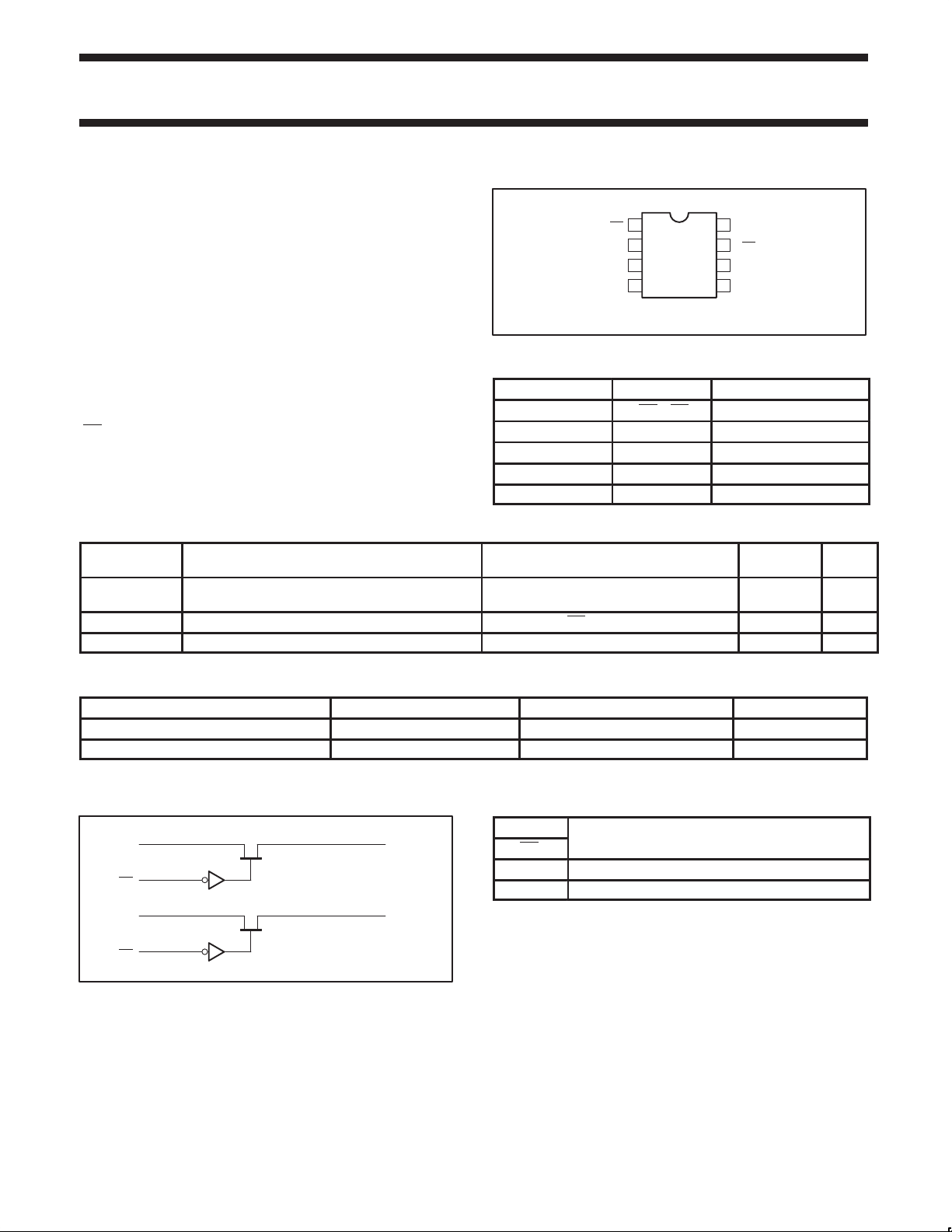
PIN CONFIGURATION
1
1OE
2
1A
3
1B
45
GND
8
7
6
SA00535
V
2OE
2B
2A
CC
PIN DESCRIPTION
PIN NUMBER SYMBOL NAME AND FUNCTION
1, 7 1OE, 2OE Output enable
2, 5 1A, 2A A port inputs
3, 6 1B, 2B B port outputs
4 GND Ground (0 V)
8 V
CC
CONDITIONS
T
= 25 °C; GND = 0 V
amb
CL = 50 pF; VCC = +5.0 V ±0.5 V 0.25 (MAX) ns
CC
Positive supply voltage
TYPICAL UNIT
6.45 pF
ORDERING INFORMATION
PACKAGES TEMPERATURE RANGE ORDER CODE DWG NUMBER
8-pin plastic SO –40 to 85 °C CBT3306D SOT96-1
8-pin plastic TSSOP –40 to 85 °C CBT3306PW SOT530-1
Standard packing quantities and other packaging data is available at www.philipslogic.com/packaging.
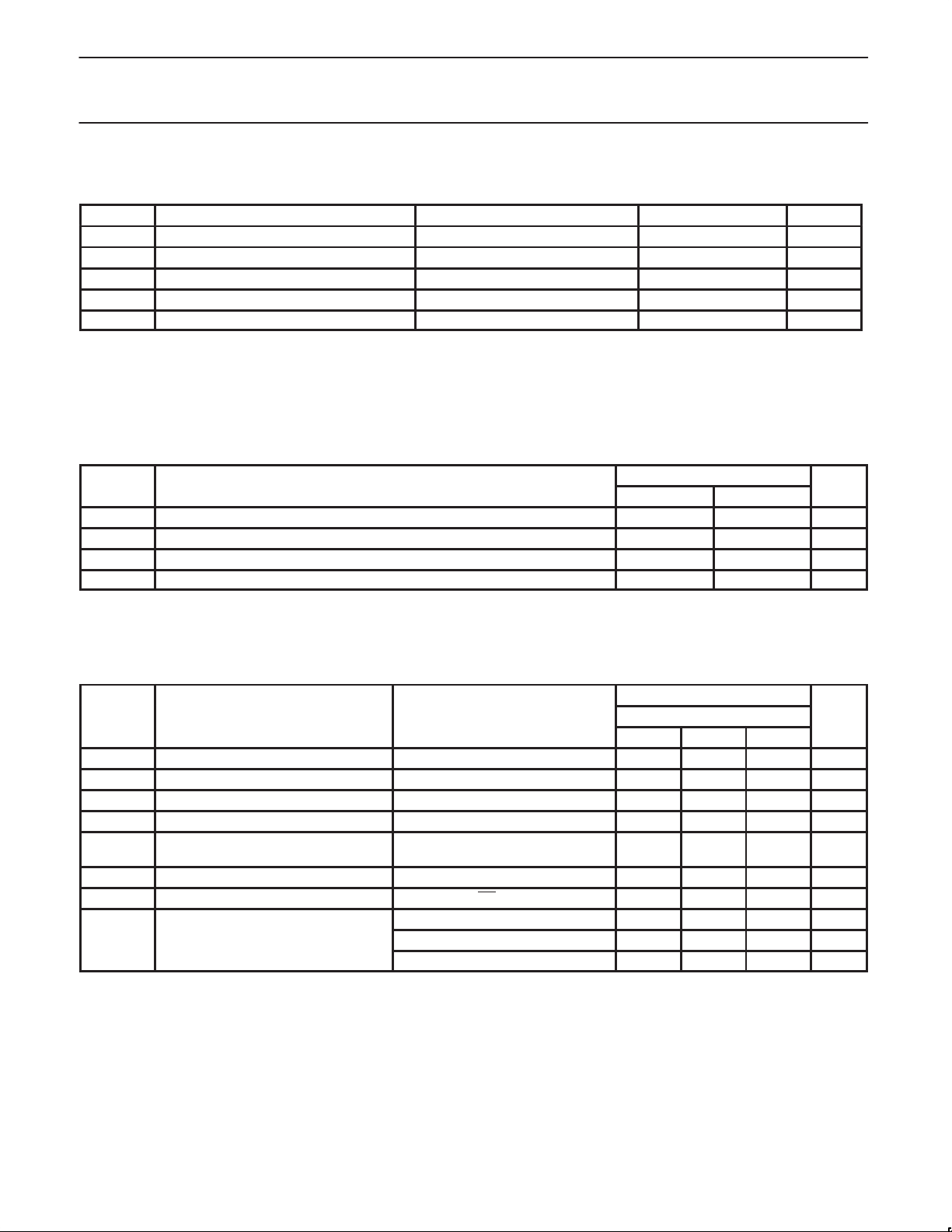
LOGIC DIAGRAM (positive logic)
2
1A
1
1OE
5
2A
7
2OE
3
1B
6
2B
SA00534
FUNCTION TABLE
INPUT
OE
L A port = B port
H Disconnect
2001 Nov 08 853-2304 27313
2
Philips Semiconductors Product data
SYMBOL
PARAMETER
UNIT
3
CBT3306Dual bus switch
ABSOLUTE MAXIMUM RATINGS
= –40 to +85 °C, unless otherwise specified.
T
amb
SYMBOL
V
CC
V
I
I
OUT
I
IK
T
stg
DC supply voltage –0.5 to +7.0 V
DC input voltage
DC output current 128 mA
Diode current V
Storage temperature range –65 to +150 °C
PARAMETER CONDITIONS RATING UNIT
2
1
–0.5 to +7.0 V
< 0 –50 mA
I/O
NOTES:
1. Stresses beyond those listed may cause permanent damage to the device. These are stress ratings only and functional operation of the
device at these or any other conditions beyond those indicated under “recommended operating conditions” is not implied. Exposure to
absolute-maximum-rated conditions for extended periods may affect device reliability .
2. The input and output negative-voltage ratings may be exceeded if the input and output clamp-current ratings are observed.
3. The package thermal impedance is calculated in accordance with JESD 51.
RECOMMENDED OPERATING CONDITIONS
1
LIMITS
MIN MAX
V
T
CC
V
V
amb
DC supply voltage 4.5 5.5 V
High-level input voltage 2.0 — V
IH
Low-level Input voltage — 0.8 V
IL
Operating free-air temperature range –40 +85 °C
NOTE:
1. All unused control inputs of the device must be held at V
or GND to ensure proper device operation.
CC
DC ELECTRICAL CHARACTERISTICS
T
= –40 to +85 °C, unless otherwise specified.
amb
SYMBOL PARAMETER TEST CONDITIONS T
V
I
∆I
C
IO(OFF)
I
CC
V
C
Input clamp voltage VCC = 4.5 V; II = –18 mA — — –1.2 V
IK
Input leakage current VCC = 5.5 V; VI = GND or 5.5 V — — ±1 µA
I
Quiescent supply current VCC = 5.5 V; IO = 0, VI = VCC or GND — — 3 µA
Output high pass voltage VI = VCC = 5.0 V; IO = –100 µA 3.4 3.6 3.9 V
P
VCC = 5.5 V, one input at 3.4 V,
Additional supply current per input pin
CC
Control pin capacitance VI= 3 V or 0 — 3.15 — pF
I
Port off capacitance VO = 3 V or 0; OE = V
2
other inputs at VCC or GND
CC
VCC = 4.5 V; VI = 0 V; II = 64 mA — 3.4 5 Ω
r
on
On-resistance
VCC = 4.5 V; VI = 0 V; II = 30 mA — 3.4 5 Ω
VCC = 4.5 V; VI = 2.4 V; II = 15 mA — 6.8 7.5 Ω
NOTES:
1. All typical values are at V
2. This is the increase in supply current for each input that is at the specified TTL voltage level rather than V
= 5 V, T
CC
amb
= 25 °C.
3. Measured by the voltage drop between the A and the B terminals at the indicated current through the switch.
On-state resistance is determined by the lowest voltage of the two (A or B) terminals.
= –40 to +85 °C UNIT
amb
MIN TYP
— — 2.5 mA
— 6.45 — pF
CC
LIMITS
or GND
1
MAX
2001 Nov 08
3
 Loading...