

Philips CBT3245A Technical data

查询CBT3245A供应商
INTEGRATED CIRCUITS
CBT3245A
Octal bus switch
Product data
Supersedes data of 2002 Feb 18
Philips
Semiconductors
2003 Jun 27

Philips Semiconductors Product data
CBT3245AOctal bus switch
2
2003 Jun 27
FEATURES
• Standard ’245-type pinout
• 5 Ω switch connection between two ports
• TTL compatible control input levels
• Package options include plastic small outline (D), shrink small
outline (DB), thin shrink small outline (TSSOP)
• Latch-up protection exceeds 500 mA per JESD78
• ESD protection exceeds 2000 V HBM per JESD22-A114,
150 V MM per JESD22-A115 and 1000 V CDM per JESD22-C101
DESCRIPTION
The CBT3245A provides eight bits of high-speed TTL-compatible
bus switching in a standard ’245 device pinout. The low on-state
resistance of the switch allows connections to be made with minimal
propagation delay.
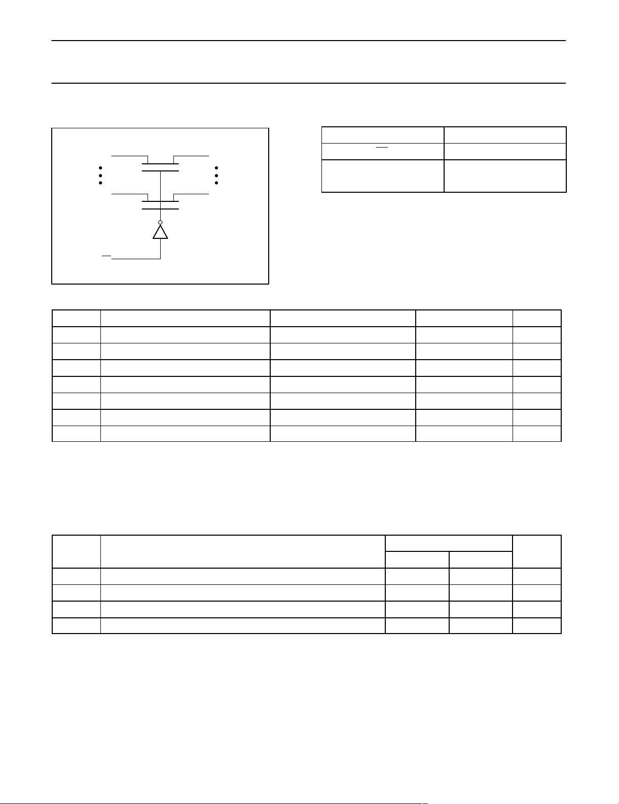
The CBT3245A device is organized as one 8-bit switch. When
enable (OE) is LOW, the switch is on and port A is connected to
port B. When OE is HIGH, the switch is open and a high-impedance
state exists between the two ports.
The CBT3245A is characterized for operation from -40 to +85 °C.
PIN CONFIGURATION — SO, SSOP, QSOP, AND
TSSOP
1
2
3
4
5
6
7
8
9
10 11
12
13
14
15
16
17
18
19
20
NC
A1
A2
A3
A4
A5
A6
A7
A8 B7
GND
B6
B5
B4
B3
B2
B1
OE
V
CC
B8
SA00507
Figure 1. Pin configuration — SO, SSOP, QSOP, and TSSOP
PIN CONFIGURATION — DHVQFN
2
1
3
4
5
6
7
8
9
10 11
12
13
14
15
16
17
18
19
20
NC
A1
A2
A3
A4
A5
A6
A7
A8 B7
GND
B6
B5
B4
B3
B2
B1
OE
V
CC
B8
SA00649
GND*
* THE DIE SUBSTRATE IS ATTACHED TO THIS PAD USING CONDUCTIVE DIE
ATTACH MATERIAL. IT CANNOT BE USED AS A SUPPLY PIN OR INPUT.
** PIN 1 INDICATION DOT
**
Figure 2. Pin configuration — DHVQFN (top view)
PIN DESCRIPTION
PIN NUMBER SYMBOL NAME AND FUNCTION
1 NC No internal connection
19 OE Output enable input
2, 3, 4, 5, 6, 7, 8, 9 A1-A8 Inputs
18, 17, 16, 15, 14,
13, 12, 11
B1-B8 Outputs
10 GND Ground (0V)
20 V
CC
Positive supply voltage
ORDERING INFORMATION
PACKAGES TEMPERATURE RANGE ORDER CODE TOPSIDE MARK DWG NUMBER
20-Pin Plastic DHVQFN -40 to 85 °C CBT3245ABQ CT3245A SOT764-1
20-Pin Plastic TSSOP -40 to 85 °C CBT3245APW CT3245A SOT360-1
20-Pin Plastic SSOP (QSOP) -40 to 85 °C CBT3245ADS CT3245ADS SOT724-1
20-Pin Plastic SSOP -40 to 85 °C CBT3245ADB CT3245A SOT339-1
20-Pin Plastic SO -40 to 85 °C CBT3245AD CBT3245AD SOT163-1
Standard packing quantities and other packaging data is available at www.philipslogic.com/packaging.
Philips Semiconductors Product data
CBT3245AOctal bus switch
2003 Jun 27
3
LOGIC SYMBOL
SA00508
A1
A8
B1
B8
2
9
18
11
19
OE
FUNCTION TABLE
INPUT INPUTS/OUTPUTS
OE A, B
L A = B
H Z
H = HIGH voltage level
L = LOW voltage level
Z = HIGH impedance “off” state
ABSOLUTE MAXIMUM RATINGS
1, 2
SYMBOL PARAMETER CONDITIONS RATING UNIT
V
CC
DC supply voltage -0.5 to +7.0 V
I
IK
DC input diode current V
I
< 0 -50 mA
V
I
DC input voltage
3
-0.5 to +7.0 V
I
OK
DC output diode current VO < 0 -50 mA
V
OUT
DC output voltage
3
output in Off or HIGH state -0.5 to +7 V
I
OUT
DC output current output in LOW state 128 mA
T
stg
Storage temperature range -65 to 150 °C
NOTES:
1. Stresses beyond those listed may cause permanent damage to the device. These are stress ratings only and functional operation of the
device at these or any other conditions beyond those indicated under “recommended operating conditions” is not implied. Exposure to
absolute-maximum-rated conditions for extended periods may affect device reliability.
2. The performance capability of a high-performance integrated circuit in conjunction with its thermal environment can create junction
temperatures which are detrimental to reliability. The maximum junction temperature of this integrated circuit should not exceed 150 °C.
3. The input and output voltage ratings may be exceeded if the input and output current ratings are observed.
RECOMMENDED OPERATING CONDITIONS
LIMITS
SYMBOL PARAMETER
MIN MAX
UNIT
V
CC
DC supply voltage 4.0 5.5 V
V
IH
HIGH-level input voltage 2.0 — V
V
IL
LOW-level input voltage — 0.8 V
T
amb
Operating free-air temperature range -40 +85 °C
Philips Semiconductors Product data
CBT3245AOctal bus switch
2003 Jun 27
4
DC ELECTRICAL CHARACTERISTICS
LIMITS
SYMBOL PARAMETER TEST CONDITIONS T
amb
= -40 to +85 °C UNIT
MIN TYP
1
MAX
V
IK
Input clamp voltage VCC = 4.5 V; II = -18 mA — — -1.2 V
I
I
Input leakage current VCC = 5.5 V; VI = GND or 5.5 V — — ±5 µA
I
CC
Quiescent supply current VCC = 5.5 V; IO = 0, VI = VCC or GND — 1 3 µA
∆I
CC
Additional supply current per
input pin
2
VCC = 5.5 V, one input at 3.4 V, other inputs at
VCC or GND
— — 3.5 mA
C
I
Control pins VI= 3 V or 0, OE = V
CC
— 3.2 — pF
C
IO(OFF)
Pin capacitance (OFF state) VO = 3 V or 0 — 6.6 — pF
VCC = 4.5 V; V1 = 0 V; II = 64 mA — 5 7
r
on
3
On-resistance VCC = 4.5 V; V1 = 0 V; II = 30 mA — 5 7 Ω
VCC = 4.5 V; V1 = 2.4 V; II = 15 mA — 10 15
NOTES:
1. All typical values are at VCC = 5 V, T
amb
= 25 °C
2. This is the increase in supply current for each input that is at the specified TTL voltage level rather than VCC or GND
3. Measured by the voltage drop between the A and the B terminals at the indicated current through the switch.
On-state resistance is determined by the lowest voltage of the two (A or B) terminals.
AC CHARACTERISTICS
GND = 0 V; tR; CL = 50 pF
CBT3245A
SYMBOL PARAMETER
FROM
(INPUT)
TO
(OUTPUT)
T
amb
= -40 to +85 °C
VCC = +5.0 V ±0.5 V
UNIT
MIN MAX
t
pd
Propagation delay
1
A or B B or A — 0.25 ns
t
en
Output enable time
to HIGH and LOW level
OE A or B 1.0 5.9 ns
t
dis
Output disable time
from HIGH and LOW level
OE A or B 1.0 6.0 ns
NOTES:
1. This parameter is warranted but not production tested. The propagation delay is based on the RC time constant of the typical on-state
resistance of the switch and a load capacitance of 50 pF, when driven by an ideal voltage source (zero output impedance).
 Loading...