

Philips CBT3125 Technical data
查询CBT3125D供应商查询CBT3125D供应商
INTEGRATED CIRCUITS
CBT3125
Quadruple FET bus switch
Product data
File under Integrated Circuits — ICL03
2001 Dec 12
Philips Semiconductors Product data
CBT3125Quadruple FET bus switch
DESCRIPTION
The CBT3125 quadruple FET bus switch features independent line
switches. Each switch is disabled when the associated Output
Enable (OE
) input is HIGH.
FEATURES
•Standard ’125-type pinout (D, DB, and PW packages)
•5 Ω switch connection between two ports
•TTL-compatible input levels
•Latch-up testing is done to JESDEC Standard JESD78 which
exceeds 500 mA
•ESD protection exceeds 2000 V HBM per JESD22-A114,
200 V MM per JESD22-A115, and 1000 V CDM per
JESD22-C101
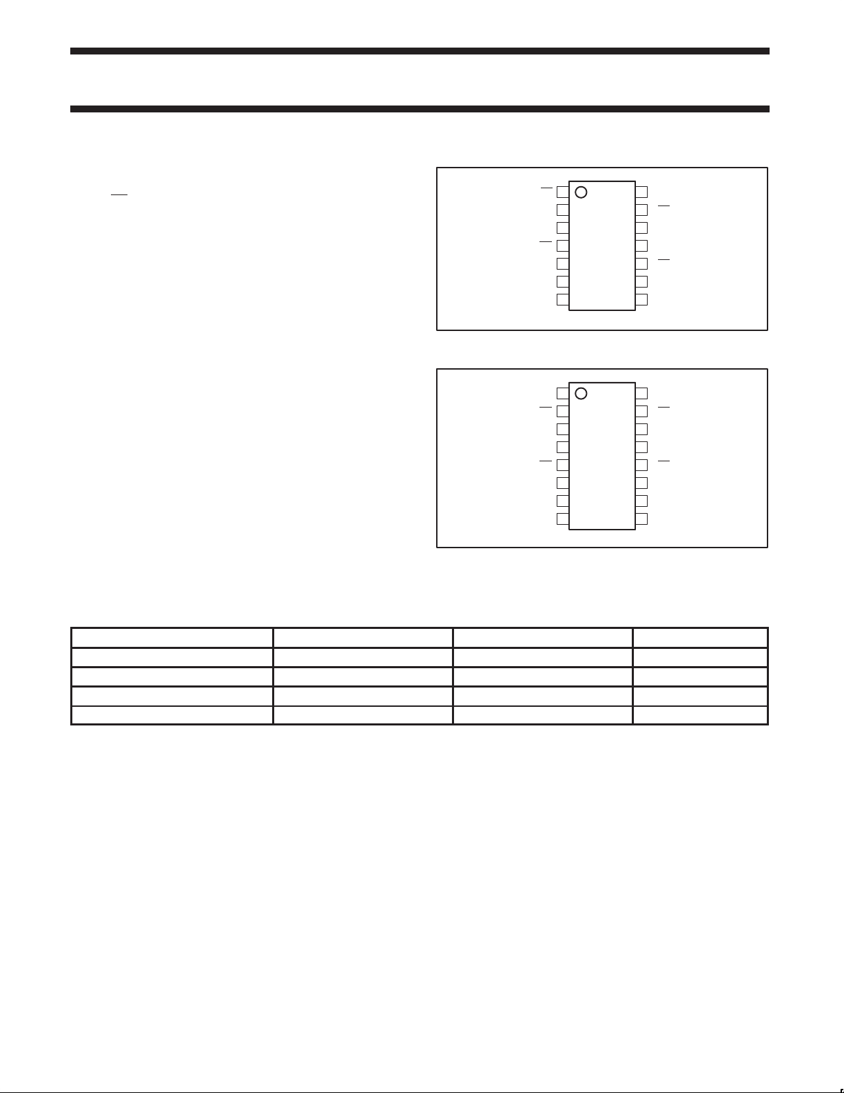
PIN CONFIGURATION
1
2
1A
3
1B
4
2OE
5
2A
6
2B
78
GND
Figure 1. SO14, SSOP14, and TSSOP14
1
2
1OE
3
1A
4
1B
5
2OE
6
2A
7
2B
89
GND
NC = no internal connection
Figure 2. SSOP(QSOP)16
141OE
13
12
11
10
SA00562
16NC
15
14
13
12
11
10
SA00563
V
CC
4OE
4A
4B
3OE
9
3A
3B
V
CC
4OE
4A
4B
3OE
3A
3B
NC
ORDERING INFORMATION
PACKAGES TEMPERATURE RANGE ORDER CODE DRAWING NUMBER
14-Pin Plastic SO –40 to +85 °C CBT3125D SOT108-1
14-Pin Plastic SSOP –40 to +85 °C CBT3125DB SOT337-1
16-Pin Plastic SSOP(QSOP) –40 to +85 °C CBT3125DS SOT519-1
14-Pin Plastic TSSOP –40 to +85 °C CBT3125PW SOT402-1
Standard packing quantities and other packaging data is available at www.philipslogic.com/packaging.
2001 Dec 12 853-2309 27452
2
Philips Semiconductors Product data
CBT3125Quadruple FET bus switch
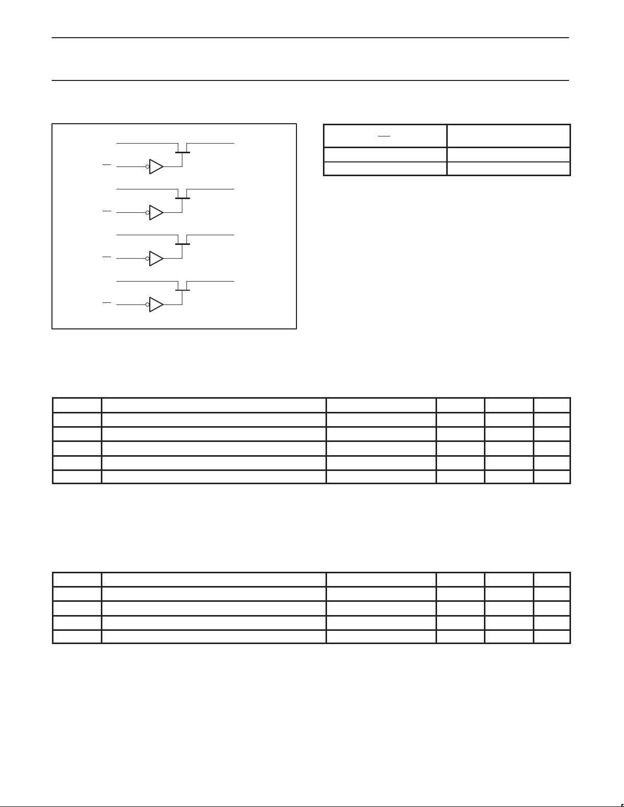
LOGIC DIAGRAM
2
1A
1
1OE
5
2A
4
2OE
9
3A
10
3OE
12
4A
13
4OE
3
6
8
11
SA00564
1B
2B
3B
4B
FUNCTION TABLE (each bus switch)
INPUT
OE
L A = B
H disconnect
FUNCTION
Pin numbers shown are for 14-pin package-types.
Figure 3. CBT3125 logic diagram (positive logic)
ABSOLUTE MAXIMUM RATINGS
1
Over operating free-air temperature range, unless otherwise noted.
SYMBOL
V
CC
V
I
supply voltage range –0.5 7 V
input voltage range see Note 2 –0.5 7 V
PARAMETER CONDITIONS MIN. MAX. UNIT
continuous channel current — 128 mA
I
T
stg
input clamp current V
K
< 0 — –50 mA
I/O
storage temperature range –65 +150 °C
NOTES:
1. Stresses beyond those listed under “absolute maximum ratings” may cause permanent damage to the device. These are stress ratings only,
and functional operation of the device at these or any other conditions beyond those indicated under “recommended operating conditions”
is not implied. Exposure to absolute-maximum-rated conditions for extended periods may affect device reliability .
2. The input and output negative-voltage ratings may be exceeded if the input and output clamp-current ratings are observed.
3. The package thermal impedance is calculated in accordance with JESD 51-7.
RECOMMENDED OPERATING CONDITIONS
SYMBOL
T
V
V
CC
V
amb
supply voltage 4.5 5.5 V
high-level control input voltage 2 — V
IH
low-level control input voltage — 0.8 V
IL
operating ambient temperature in free-air –40 +85 °C
NOTE:
1. All unused control inputs of the device must be held at V
2001 Dec 12
PARAMETER CONDITIONS MIN. MAX. UNIT
1
or GND to ensure proper device operation.
CC
3
 Loading...