

Philips CBT16213 Technical data
查询CBT16213供应商
INTEGRATED CIRCUITS
CBT16213
24-bit bus exchange switch
with 12-bit output enables
Objective specification 2001 Jan 19
Philips Semiconductors Objective specification
24-bit bus exchange switch
with 12-bit output enables
FEATURES
•5 Ω switch connection between two ports
•TTL compatible control input levels
•Package options include plastic shrink small outline (SSOP) and
thin shrink small outline (TSSOP)
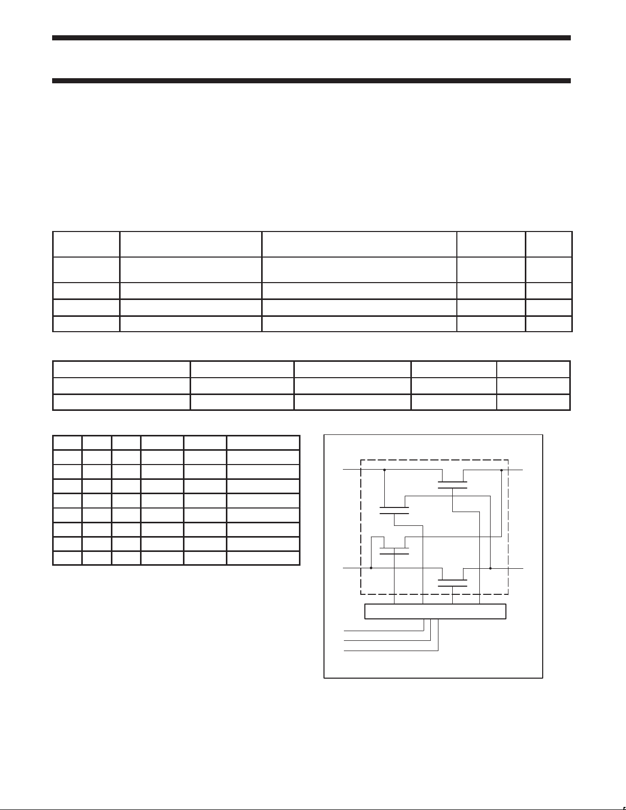
QUICK REFERENCE DATA
SYMBOL PARAMETER
C
t
PLH
t
PHL
C
OUT
I
CCZ
IN
Propagation delay
An to Yn
Input capacitance VI = 0 V or V
Output capacitance Outputs disabled; VO = 0 V or V
Total supply current Outputs disabled; VCC = 5.5 V 3 µA
CL = 50 pF; VCC = 5 V 0.25 ns
CBT16213
DESCRIPTION
The CBT16213 provides 24 bits of high-speed TTL-compatible bus
switching or exchanging. The low on-state resistance of the switch
allows connections to be made with minimal propagation delay.
The CBT16213 operates as 24-bit bus switch or a 12-bit bus
exchanger, which provides data exchanging between the four signal
ports via the data-select (S0–S2) terminals.
The CBT16213 is characterized for operation from –40 to +85 °C.
CONDITIONS
T
= 25 °C; GND = 0 V
amb
CC
CC
TYPICAL UNIT
4.5 pF
11.5 pF
ORDERING INFORMATION
PACKAGES TEMPERATURE RANGE OUTSIDE NORTH AMERICA NORTH AMERICA DWG NUMBER
56-Pin Plastic SSOP Type III –40 to +85 °C CBT16213DL CBT16213DL SOT371-1
56-Pin Plastic TSSOP Type II –40 to +85 °C CBT16213DGG CBT16213DGG SOT364-1
FUNCTION TABLE
S2 S1 S0 A1 A2 FUNCTION
L L L Z Z Disconnect
L L H B1 Z A1 = B1
L H L B2 Z A1 = B2
L H H Z B1 A2 = B1
H L L Z B2 A2 = B2
H L H A2 & B2 A1 & B2 A1 = A2 = B2
H H L B1 B2 A1 = B1, A2 = B2
H H H B2 B1 A1 = B2, A2 = B1
H = High voltage level
L = Low voltage level
Z = High impedance “off” state
LOGIC SYMBOL
254
1A1
353
1A2
1
S0
56
S1
55
S2
1 of 12 Channels
FLOW CONTROL
1B1
1B2
2001 Jan 19
SA00512
2
Philips Semiconductors Objective specification
24-bit bus exchange switch
with 12-bit output enables
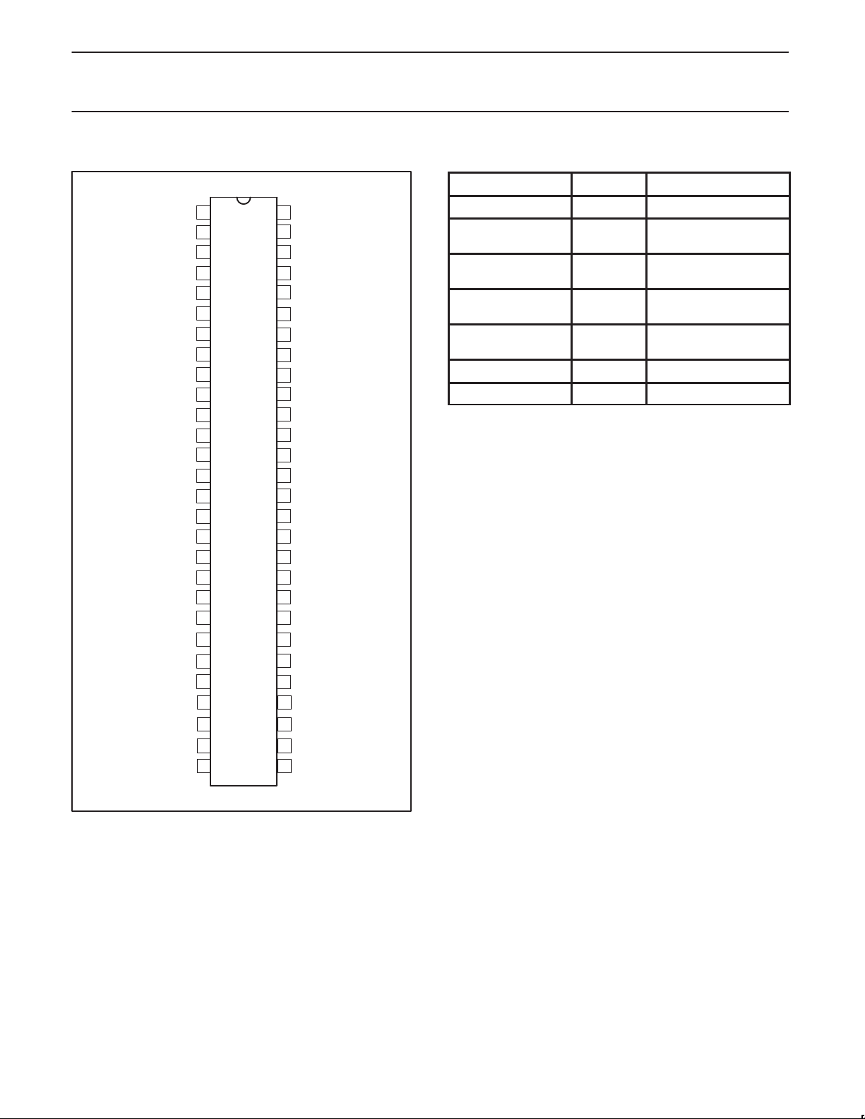
PIN CONFIGURATION
1A1
1A2
2A1
2A2
3A1
3A2
GND
4A1
4A2
5A1
5A2
6A1
6A2
7A1
7A2
V
8A1
GND
8A2
9A1
9A2
10A1
10A2
11A1
11A2
12A1
12A2
1
S0
2
3
4
5
6
7
8
9
10
11
12
13
14
15
16
17
CC
18
19
20
21
22
23
24
25
26
27
28
56
55
54
53
52
51
50
49
48
47
46
45
44
43
42
41
40
39
38
37
36
35
34
33
32
31
30
29
S1
S2
1B1
1B2
2B1
2B2
3B1
GND
3B2
4B1
4B2
5B1
5B2
6B1
6B2
7B1
7B2
8B1
GND
8B2
9B1
9B2
10B1
10B2
11B1
11B2
12B1
12B2
CBT16213
PIN DESCRIPTION
PIN NUMBER SYMBOL NAME AND FUNCTION
1, 56, 55 S0, S1, S2 Data select
2, 4, 6, 9, 11, 13, 15,
18, 21, 23, 25, 27
3, 5, 7, 10, 12, 14, 16,
20, 22, 24, 26, 28
54, 52, 50, 47, 45, 43,
41, 39, 36, 34, 32, 30
53, 51, 48, 46, 44, 42,
40, 37, 35, 33, 31, 29
8, 19, 38, 49 GND Ground (0 V)
17 V
1A1–12A1 A1 channel
1A2–12A2 A2 channel
1B1, 12B1 B1 channel
1B2, 12B2 B2 channel
CC
Positive supply voltage
2001 Jan 19
SA00511
3
 Loading...