Philips CBT16211 Technical data

查询CBT16211供应商查询CBT16211供应商
INTEGRATED CIRCUITS
CBT16211
24-bit bus switch with 12-bit output enables
Product data
2001 Jun 13

Philips Semiconductors Product data
CBT1621 124-bit bus switch with 12-bit output enables
FEA TURES
•5 Ω switch connection between two ports
•TTL compatible control input levels
•Package options include plastic shrink small outline (SSOP),
thin shrink small outline (TSSOP)
•ESD protection exceeds 1000 V CDM per JESD22-C101
•Latch-up testing is done to JESDEC Standard JESD78 which
exceeds 100 mA
DESCRIPTION
The CBT16211 provides 24 bits of high-speed TTL-compatible bus
switching. The low on-state resistance of the switch allows
connections to be made with minimal propagation delay.
The device is organized as a dual 12-bit bus switch with separate
output-enable (OE
or as one 24-bit bus switch. When OE
bus switch is on, and port A is connected to port B. When OE
high, the switch is open, and a high-impedance state exists between
the ports.
) inputs. It can be used as two 12-bit bus switches
is low, the associated 12-bit
The CBT16211 is characterized for operation from –40 to 85 °C.
QUICK REFERENCE DAT A
SYMBOL PARAMETER
C
t
PLH
t
PHL
C
I
IN
OUT
CC
Propagation delay
An to Yn
Input capacitance VI = 0 V or V
Output capacitance Outputs disabled; VO = 0 V or V
Total supply current Outputs disabled; VCC = 5.5 V 3.0 µA
CL = 50 pF; VCC = 5 V 0.25 ns
CONDITIONS
T
= 25 °C; GND = 0 V
amb
CC
CC
TYPICAL UNIT
4.3 pF
6.9 pF
ORDERING INFORMATION
PACKAGES TEMPERATURE RANGE ORDER CODE DWG NUMBER
56-Pin Plastic SSOP Type III –40 to 85 °C CBT16211DL SOT371-1
56-Pin Plastic TSSOP Type II –40 to 85 °C CBT16211DGG SOT364-1
is
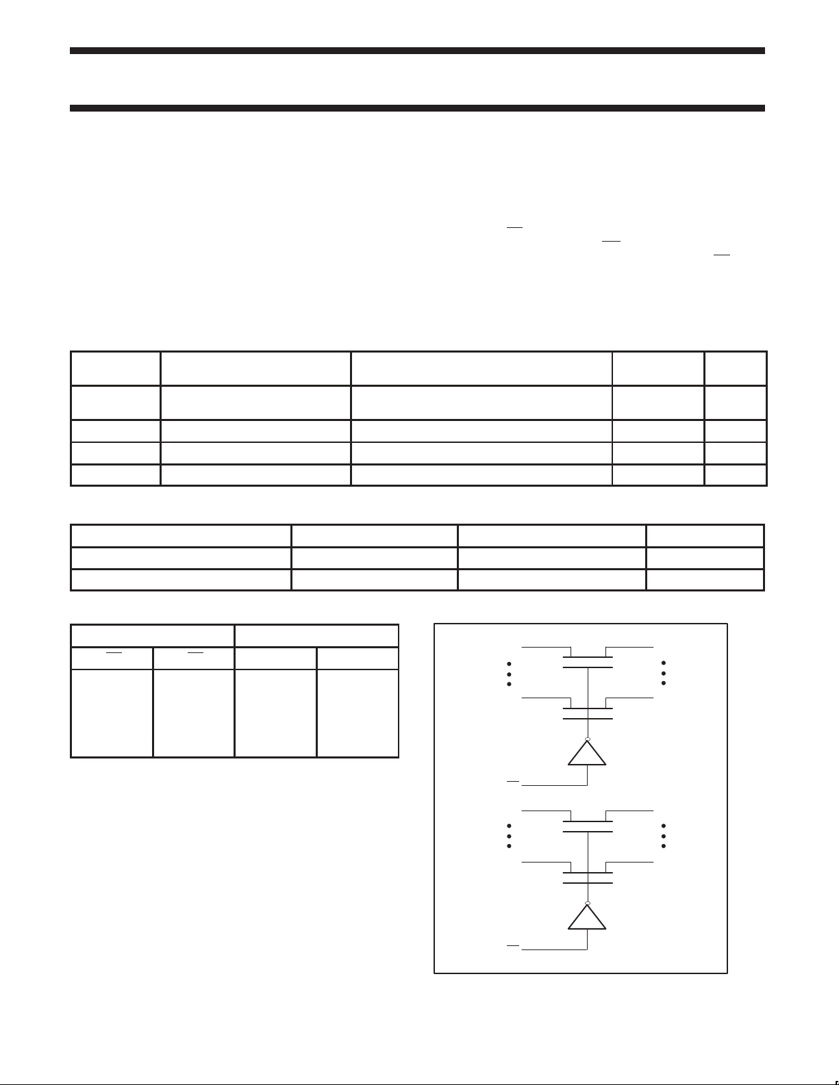
FUNCTION TABLE
INPUTS OUTPUTS
1OE 2OE 1A, 1B 2A, 2B
L L 1A = 1B 2A = 2B
L H 1A = 1B Z
H L Z 2A = 2B
H H Z Z
H = High voltage level
L = Low voltage level
Z = High impedance “off” state
LOGIC SYMBOL
2
1A1
14
1A12
56
1OE
15
2A1
28
2A12
55
2OE
54
1B1
42
1B12
41
2B1
29
2B12
SA00510
2001 Jun 13 853-2259 26502
2

Philips Semiconductors Product data
CBT1621124-bit bus switch with 12-bit output enables
PIN CONFIGURATION
1
NC
1A1
2
3
1A2
1A3
4
5
1A4
1A5
6
1A6
7
8
GND
1A7
9
10
1A8
1A9
11
12
1A10
1A11
13
14
1A12
2A1
15
2A2
16
17
V
CC
18
2A3
19
GND
20
2A4
21
2A5
22
2A6
23
2A7
24
2A8
25
2A9
26
2A10
27
2A11
2A12
28
PIN DESCRIPTION
PIN NUMBER SYMBOL NAME AND FUNCTION
56
1OE
55
2OE
54
1B1
1B2
53
52
1B3
1B4
51
1B5
50
GND
49
1B6
48
47
1B7
46
1B8
45
1B9
44
1B10
43
1B11
1B12
42
2B1
41
40
2B2
39
2B3
38
GND
37
2B4
36
2B5
35
2B6
34
2B7
33
2B8
32
2B9
31
2B10
30
2B11
2B12
29
2, 3, 4, 5, 6, 7, 9, 10,
54, 53, 52, 51, 50, 48,
47, 46, 45, 44, 43, 42
15, 16, 18, 20, 21, 22,
23, 24, 25, 26, 27, 28
41, 40, 39, 37, 36, 35,
34, 33, 32, 31, 30, 29
1 NC No internal connection
56, 55 1OE, 2OE Output Enables
11, 12, 13, 14
1A1-1A12 Inputs
1B1-1B12 Outputs
2A1-2A12 Inputs
2B1-2B12 Outputs
8, 19, 38, 49 GND Ground (0 V)
17 V
CC
Positive supply voltage
2001 Jun 13
SA00509
3
 Loading...