

Philips BZW03-C91, BZW03-C22, BZW03-C200-20, BZW03-C43, BZW03-C39 Datasheet
...
DATA SH EET
Product specification
Supersedes data of April 1992
1996 May 14
DISCRETE SEMICONDUCTORS
BZW03 series
Voltage regulator diodes
handbook, 2 columns
M3D118
1996 May 14 2
Philips Semiconductors Product specification
Voltage regulator diodes BZW03 series
FEATURES
• Glass passivated
• High maximum operating
temperature
• Low leakage current
• Excellent stability
• Zener working voltage range:
7.5 to 270 V for 38 types
• Transient suppressor stand-off
voltage range:
6.2 to 430 V for 45 types
• Available in ammo-pack
• Also available with preformed leads
for easy insertion.
DESCRIPTION
Rugged glass SOD64 package, using
a high temperature alloyed
construction. This package is
hermetically sealed and fatigue free
as coefficients of expansion of all
used parts are matched.
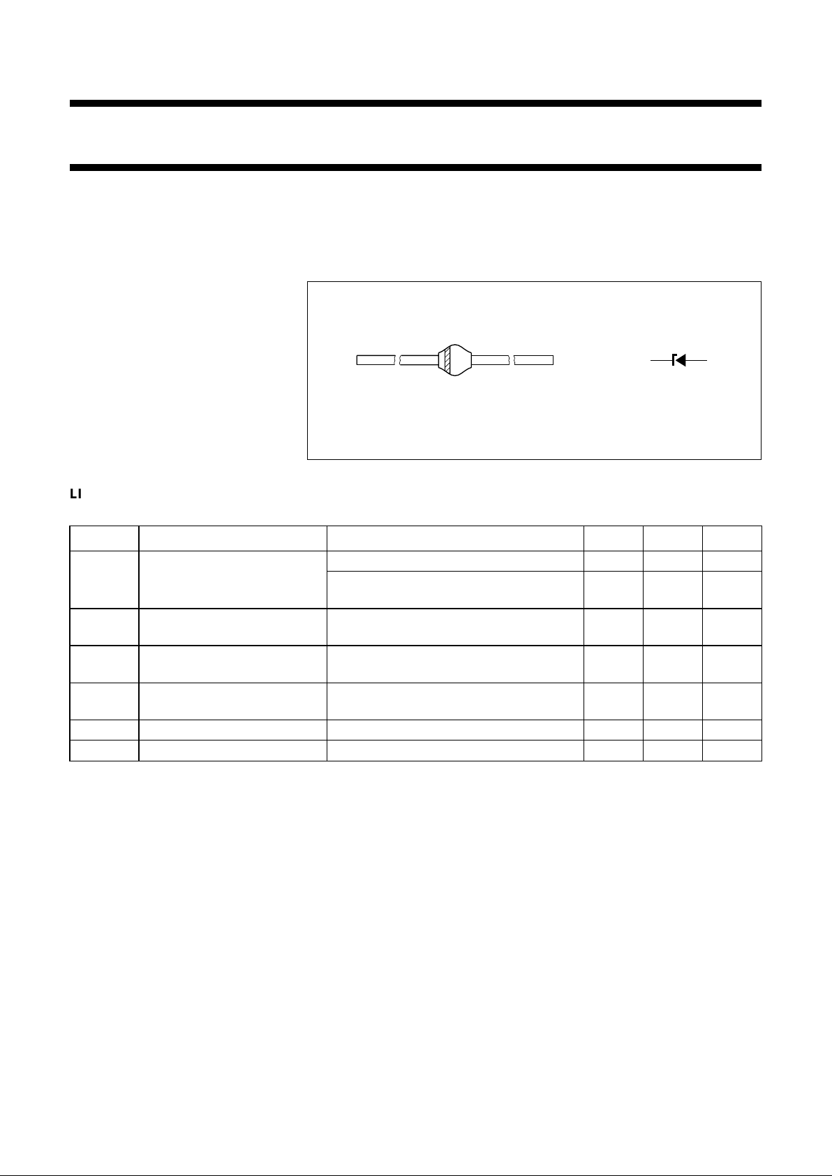
Fig.1 Simplified outline (SOD64) and symbol.
2/3 page (Datasheet)
MAM205
ka
LIMITING VALUES
In accordance with the Absolute Maximum Rating System (IEC 134).
SYMBOL PARAMETER CONDITIONS MIN. MAX. UNIT
P
tot
total power dissipation Ttp=25°C; lead length 10 mm; see Fig.2 − 6.00 W
T
amb
=45°C; see Fig.2;
PCB mounted (see Fig.6)
− 1.75 W
P
ZRM
repetitive peak reverse power
dissipation
− 20 W
P
ZSM
non-repetitive peak reverse
power dissipation
tp= 100 µs; square pulse;
Tj=25°C prior to surge; see Fig.3
− 1000 W
P
RSM
non-repetitive peak reverse
power dissipation
10/1000 µs exponential pulse (see Fig.7);
Tj=25°C prior to surge; see Fig.4
− 500 W
T
stg
storage temperature −65 +175 °C
T
j
junction temperature −65 +175 °C
1996 May 14 3
Philips Semiconductors Product specification
Voltage regulator diodes BZW03 series
ELECTRICAL CHARACTERISTICS
Total series
T
j
=25°C unless otherwise specified.
Per type when used as voltage regulator diodes
T
j
=25°C unless otherwise specified.
SYMBOL PARAMETER CONDITIONS MAX. UNIT
V
F
forward voltage IF= 1 A; see Fig.5 1.2 V
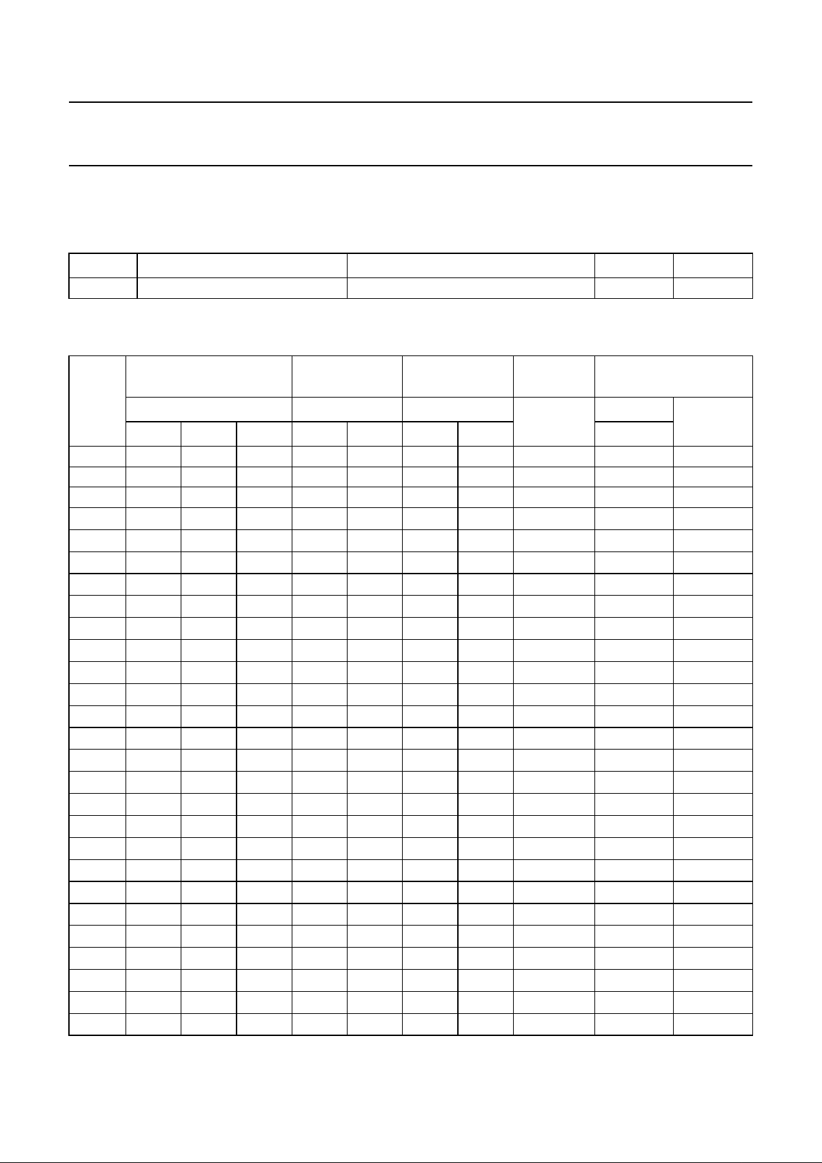
TYPE
No.
SUFFIX
(1)
WORKING VOLTAGE
DIFFERENTIAL
RESISTANCE
TEMPERATURE
COEFFICIENT
TEST
CURRENT
REVERSE CURRENT at
REVERSE VOLTAGE
VZ (V) at I
Z
r
dif
(Ω)atI
Z
SZ (%/K) at I
Z
IZ (mA)
IR (µA)
at VR (V)
MIN. NOM. MAX. TYP. MAX. MIN. MAX. MAX.
C7V5 7.0 7.5 7.9 0.7 1.5 0.00 0.07 175 1500 5.6
C8V2 7.7 8.2 8.7 0.8 1.5 0.03 0.08 150 1200 6.2
C9V1 8.5 9.1 9.6 0.9 2.0 0.03 0.08 150 40 6.8
C10
9.4 10 10.6 1.0 2.0 0.05 0.09 125 20 7.5
C11
10.4 11 11.6 1.1 2.5 0.05 0.10 125 15 8.2
C12
11.4 12 12.7 1.1 2.5 0.05 0.10 100 10 9.1
C13
12.4 13 14.1 1.2 2.5 0.05 0.10 100 4 10
C15
13.8 15 15.6 1.2 2.5 0.05 0.10 75 2 11
C16
15.3 16 17.1 1.3 2.5 0.06 0.11 75 2 12
C18
16.8 18 19.1 1.3 2.5 0.06 0.11 65 2 13
C20
18.8 20 21.2 1.5 3.0 0.06 0.11 65 2 15
C22
20.8 22 23.3 1.6 3.5 0.06 0.11 50 2 16
C24
22.8 24 25.6 1.8 3.5 0.06 0.11 50 2 18
C27
25.1 27 28.9 2.5 5 0.06 0.11 50 2 20
C30
28 30 32 4 8 0.06 0.11 40 2 22
C33
31 33 35 5 10 0.06 0.11 40 2 24
C36
34 36 38 6 11 0.06 0.11 30 2 27
C39
37 39 41 7 14 0.06 0.11 30 2 30
C43
40 43 46 10 20 0.07 0.12 30 2 33
C47
44 47 50 12 25 0.07 0.12 25 2 36
C51
48 51 54 14 27 0.07 0.12 25 2 39
C56
52 56 60 18 35 0.07 0.12 20 2 43
C62
58 62 66 20 42 0.08 0.13 20 2 47
C68
64 68 72 22 44 0.08 0.13 20 2 51
C75
70 75 79 25 45 0.08 0.13 20 2 56
C82
77 82 87 30 65 0.08 0.13 15 2 62
C91
85 91 96 40 75 0.09 0.13 15 2 68
 Loading...