

Philips BZA456A Datasheet
DISCRETE SEMICONDUCTORS
DATA SH EET
ook, halfpage
M3D302
BZA456A
Quadruple ESD transient voltage
suppressor
Product specification
Supersedes data of 1998 Oct 30
1999 May 25
Philips Semiconductors Product specification
Quadruple ESD transient voltage suppressor BZA456A
FEATURES
• ESD rating >8 kV, according to IEC1000-4-2
• SOT457 surface mount package
• Common anode configuration
• Non-clamping range −0.5 to 5.6 V
• Maximum reverse peak power dissipation:
24 W at tp=1ms
• Maximum clamping voltage at peak pulse current:
8 V at I
ZSM
=3A.
APPLICATIONS
• Computers and peripherals
• Audio and video equipment
• Communication systems
• Medical equipment.
DESCRIPTION
Monolithic transient voltage suppressor diode in a six lead
SOT457 (SC-74) package for 4-bit wide ESD transient
suppression at 5.6 V level.
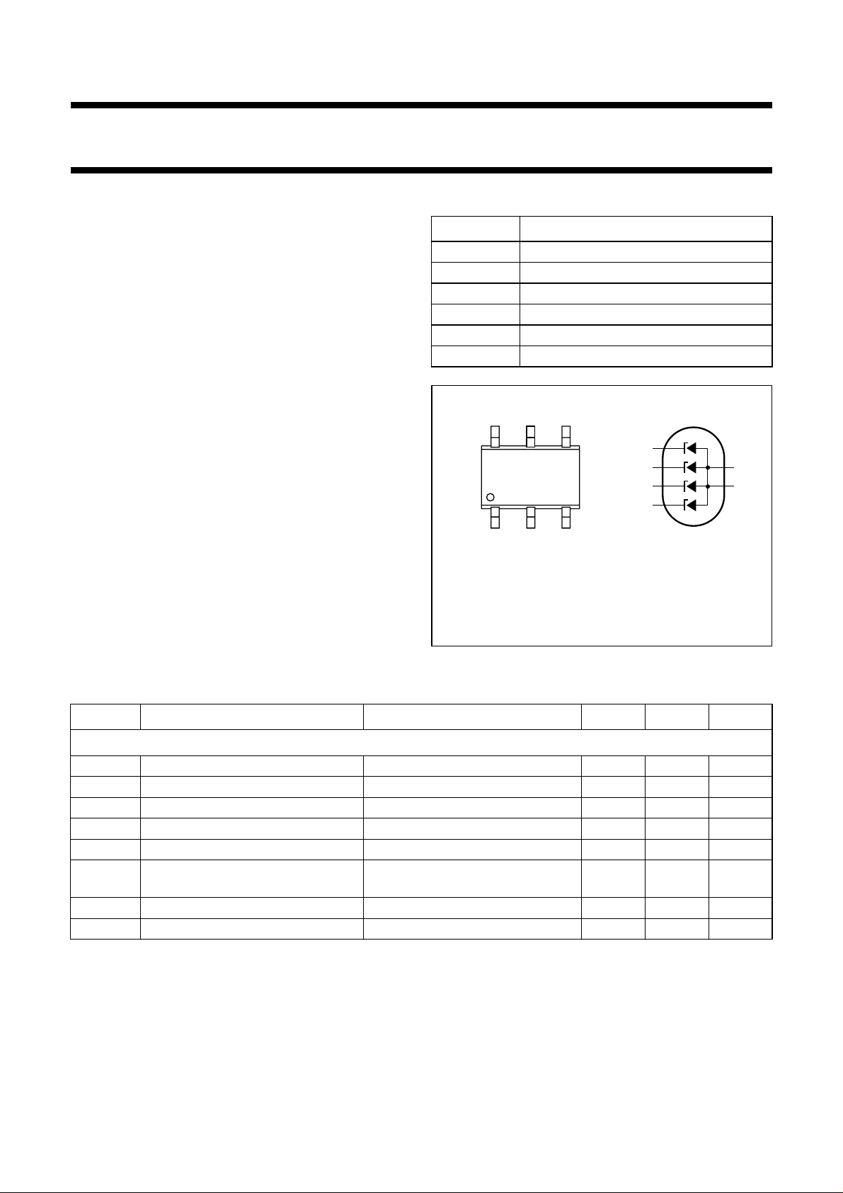
PINNING
PIN DESCRIPTION
1 cathode 1
2 common
3 cathode 2
4 cathode 3
5 common
6 cathode 4
handbook, halfpage
132
Top view
Marking code: Z6.
56
4
1
3
4
6
MAM357
Fig.1 Simplified outline (SOT457) and symbol.
2
5
LIMITING VALUES
In accordance with the Absolute Maximum Rating System (IEC 134).
SYMBOL PARAMETER CONDITIONS MIN. MAX. UNIT
Per diode
I
Z
I
F
I
FSM
I
ZSM
P
tot
P
ZSM
working current Ts=60°C; note 1 − note 2 mA
continuous forward current Ts=60°C − 100 mA
non-repetitive peak forward current tp= 1 ms; square pulse − 3.75 A
non-repetitive peak reverse current tp= 1 ms; square pulse; see Fig.2 − 3A
total power dissipation Ts=60°C; see Fig.3 − 720 mW
non repetitive peak reverse power
square pulse; tp= 1 ms; see Fig.4 − 24 W
dissipation
T
stg
T
j
storage temperature −65 +150 °C
junction temperature −65 +150 °C
Notes
1. T
is the temperature at the soldering point of the anode pin.
s
2. DC working current limited by P
tot max
.
1999 May 25 2

Philips Semiconductors Product specification
Quadruple ESD transient voltage suppressor BZA456A
THERMAL CHARACTERISTICS
SYMBOL PARAMETER CONDITIONS VALUE UNIT
R
th j-s
ELECTRICAL CHARACTERISTICS
=25°C unless otherwise specified.
T
j
SYMBOL PARAMETER CONDITIONS MIN. TYP. MAX. UNIT
Per diode
V
Z
V
F
V
ZSM
I
R
r
dif
S
Z
C
d
thermal resistance from junction to soldering point one or more diodes loaded 125 K/W
working voltage IZ= 1 mA 5.32 5.6 5.88 V
forward voltage IF= 200 mA −−1.3 V
non-repetitive peak reverse voltage I
= 3 A; tp=1ms −−8V
ZSM
reverse current VR=3V −−2µA
differential resistance IZ= 250 µA −−1600 Ω
I
=1mA −−400 Ω
Z
temperature coefficient of working
IZ=5mA − 1.2 − mV/K
voltage
diode capacitance see Fig.5
V
= 0; f = 1 MHz −−240 pF
R
V
= 3 V; f = 1 MHz −−140 pF
R
1999 May 25 3
Philips Semiconductors Product specification
Quadruple ESD transient voltage suppressor BZA456A
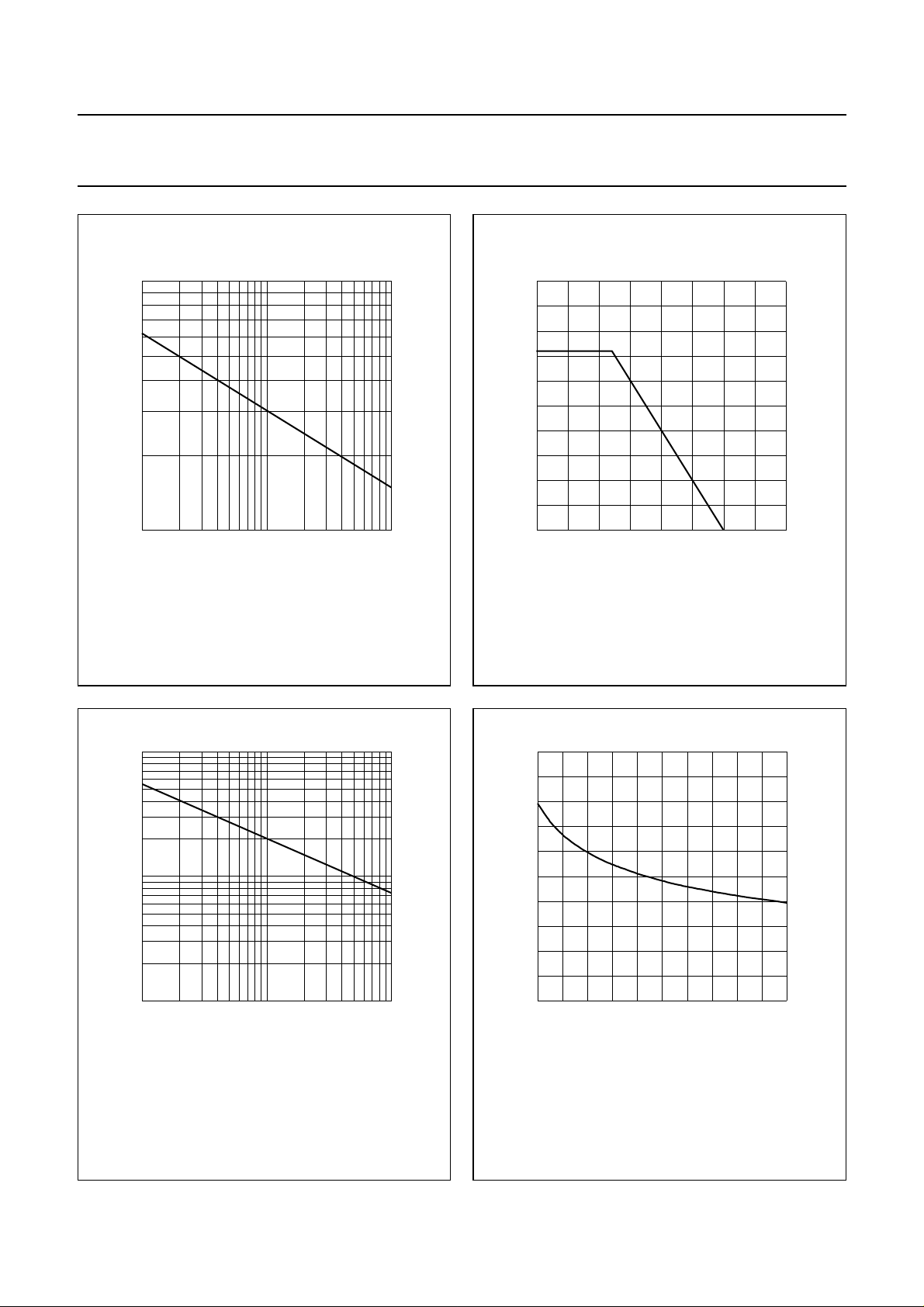
10
handbook, halfpage
I
ZSM
(A)
1
−1
10
1
tp (ms)
Fig.2 Maximum non-repetitive peak reverse
current as a function of pulse time.
MDA190
150
Ts (
MDA198
o
C)
1000
handbook, halfpage
P
tot
(mW)
800
600
400
200
10
0
0 50 100 200
All diodes loaded.
Fig.3 Power derating curve.
2
10
handbook, halfpage
P
ZSM
(W)
10
1
−1
10
P
ZSM=VZSM
V
ZSM
× I
.
is the non-repetitive peak reverse voltage at I
ZSM
110
tp (ms)
Fig.4 Maximum non-repetitive peak reverse
power dissipation as a function of pulse
duration (square pulse).
MDA199
ZSM
250
handbook, halfpage
C
d
(pF)
200
150
100
50
0
05
.
Tj=25°C; f = 1 MHz.
1234
MDA192
VR (V)
Fig.5 Diode capacitance as a function of reverse
voltage; typical values.
1999 May 25 4
 Loading...