

Philips BZA408B Datasheet
DATA SH EET
ook, halfpage
M3D302
BZA408B
Quadruple bidirectional ESD
transient voltage suppressor
Product specification
Supersedes data of 1998 Jun 05
1998 Oct 15
Philips Semiconductors Product specification
Quadruple bidirectional ESD transient
voltage suppressor
FEATURES
• ESD rating >15 kV, according to IEC1000-4-2
• SOT457 surface mount package
• Non-clamping range: −5Vto+5V
• Channel separation: >70 dB
• Low reverse current: <100 nA
• Low diode capacitance: <75 pF.
APPLICATIONS
• Protection of equipment, connected to data and
transmission lines, against voltage surges caused by
electrostatic discharge e.g:
– Computers and peripherals
– Audio and video equipment
– Communication systems
– Medical equipment
– Portable electronics.
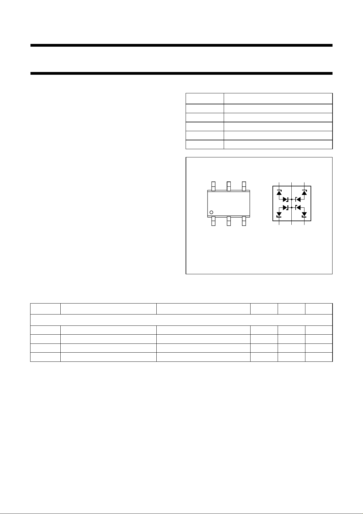
PINNING
PIN DESCRIPTION
1 cathode 1
2, 5 ground
3 cathode 2
4 cathode 3
6 cathode 4
handbook, halfpage
Top view
56
4
132
BZA408B
456
132
MAM409
DESCRIPTION
4-bit wide monolithic bidirectional ESD transient voltage
Marking code: Z8.
Fig.1 Simplified outline (SOT457) and symbol.
suppressor in a six lead SOT457 (SC-74) package.
LIMITING VALUES
In accordance with the Absolute Maximum Rating System (IEC 134).
SYMBOL PARAMETER CONDITIONS MIN. MAX. UNIT
Per diode (pin 2 and / or 5 connected to ground)
I
ZSM
P
ZSM
T
stg
T
j
non-repetitive peak reverse current tp= 1 ms; square pulse; see Fig.2 − 2A
non-repetitive peak power tp= 1 ms; square pulse − 20 W
storage temperature −65 +150 °C
junction temperature −65 +150 °C
1998 Oct 15 2

Philips Semiconductors Product specification
Quadruple bidirectional ESD transient
BZA408B
voltage suppressor
THERMAL CHARACTERISTICS
SYMBOL PARAMETER CONDITIONS VALUE UNIT
R
th j-s
ELECTRICAL CHARACTERISTICS
=25°C unless otherwise specified.
T
j
SYMBOL PARAMETER CONDITIONS MIN. MAX. UNIT
Per diode (pin 2 and / or 5 connected to ground)
V
RWM
V
R
V
ZSM
I
R
C
d
α
ch (p to p)
thermal resistance from junction to soldering point one or more diodes loaded 340 K/W
working reverse voltage − 5V
reverse voltage I
non-repetitive peak reverse voltage tp= 1 ms; I
reverse current VR=V
= 5 mA 5.5 − V
test
=2A − 10 V
ZSM
RWM
− 100 nA
diode capacitance see Fig.3
V
= 0; f = 1 MHz − 75 pF
R
= 5 V; f = 1 MHz − 55 pF
V
R
pin to pin channel separation note 1; see Fig.4 70 − dB
Note
1. α
ch (p top)
is measured as follows: a −7 dBs sinewave of 400 Hz is connected to e.g. pin 6 and a −7 dBs sinewave of
1 kHz to pin 1. The 1 kHz signal of pin 1 is measured on pin 6 by means of a spectrum analyser with an input
impedance of 1 MΩ. So α
ch (p to p)
equals the 1 kHz level on pin 1 minus the 1 kHz level on pin 6. For the 400 Hz
signal the same measurement is done in the opposite way.
1998 Oct 15 3
Philips Semiconductors Product specification
Quadruple bidirectional ESD transient
voltage suppressor
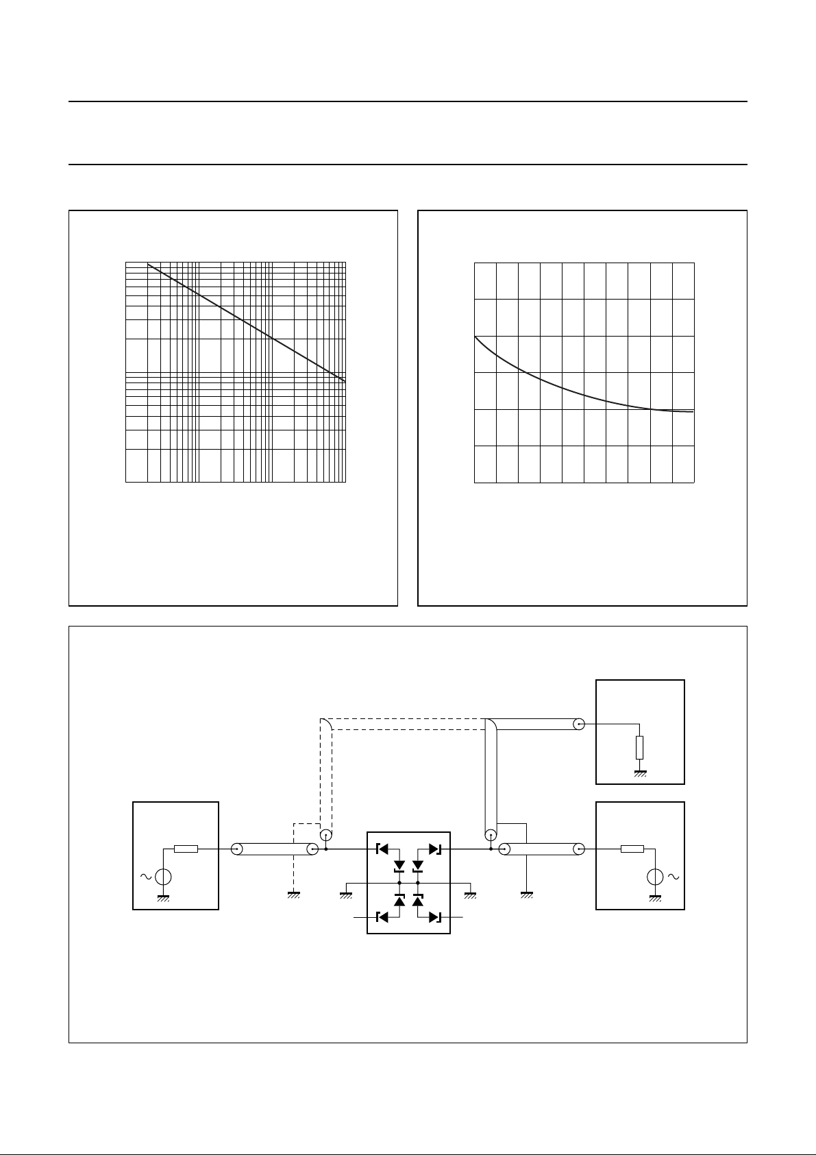
GRAPHICAL DATA
10
handbook, halfpage
I
ZSM
(A)
1
−1
10
−2
10
−1
10
110
MGR557
t
(ms)
p
80
handbook, halfpage
C
d
(pF)
60
40
20
0
BZA408B
MGR558
15
234
VR (V)
Fig.2 Maximum non-repetitive peak reverse
current as a function of pulse time.
handbook, full pagewidth
SIGNAL
GENERATOR
600 Ω
f = 1 kHz
−7 dBs
Tj=25°C; f = 1 MHz.
Fig.3 Diode capacitance as a function of reverse
voltage; typical values.
coaxial cable with
SMB connector
DUT
1
2
3
6
5
4
SPECTRUM
ANALYZER
SIGNAL
GENERATOR
600 Ω
f = 400 Hz
−7 dBs
1 MΩ
MGR556
Fig.4 Channel separation measurement setup.
1998 Oct 15 4
 Loading...