Philips BZA109TS Datasheet

DISCRETE SEMICONDUCTORS
DATA SH EET
M3D370
BZA109TS
9-fold ESD transient voltage
suppressor
Product specification
Supersedes data of 1997 Dec 11
1998 Nov 26

Philips Semiconductors Product specification
9-fold ESD transient voltage suppressor BZA109TS
FEATURES
• ESD rating >8 kV, according to
IEC1000-4-2
• SOT339-1 surface mount package
• Common anode configuration
• Non-clamping range −0.5 to +6.8 V
• Maximum non-repetitive peak
reverse power dissipation: 25 W
at tp=1ms
• Maximum clamping voltage at peak
pulse current: 10 V at I
ZSM
= 2.5 A.
APPLICATIONS
• For 9-bit wide undershoot/
overshoot clamping and fast ESD
transient suppression in:
– Computers and peripherals
– Audio and video equipment
– Business machines
– Communication systems
– Medical equipment.
DESCRIPTION
9-fold monolithic transient voltage
suppressor in an SSOP20; SOT339-1
surface mount package. The device is
ideal in situations where board space
is a premium.
handbook, 4 columns
1
2
3
4
5
6
7
8
9
10
OUT1IN1
20
OUT2IN2
19
OUT3IN3
18
OUT4IN4
17
OUT5IN5
16
GNDGND
15
14
OUT6IN6
13
OUT7IN7
12
OUT8IN8
11
OUT9IN9
Marking code: ZA109TS.
PINNING
PIN DESCRIPTION
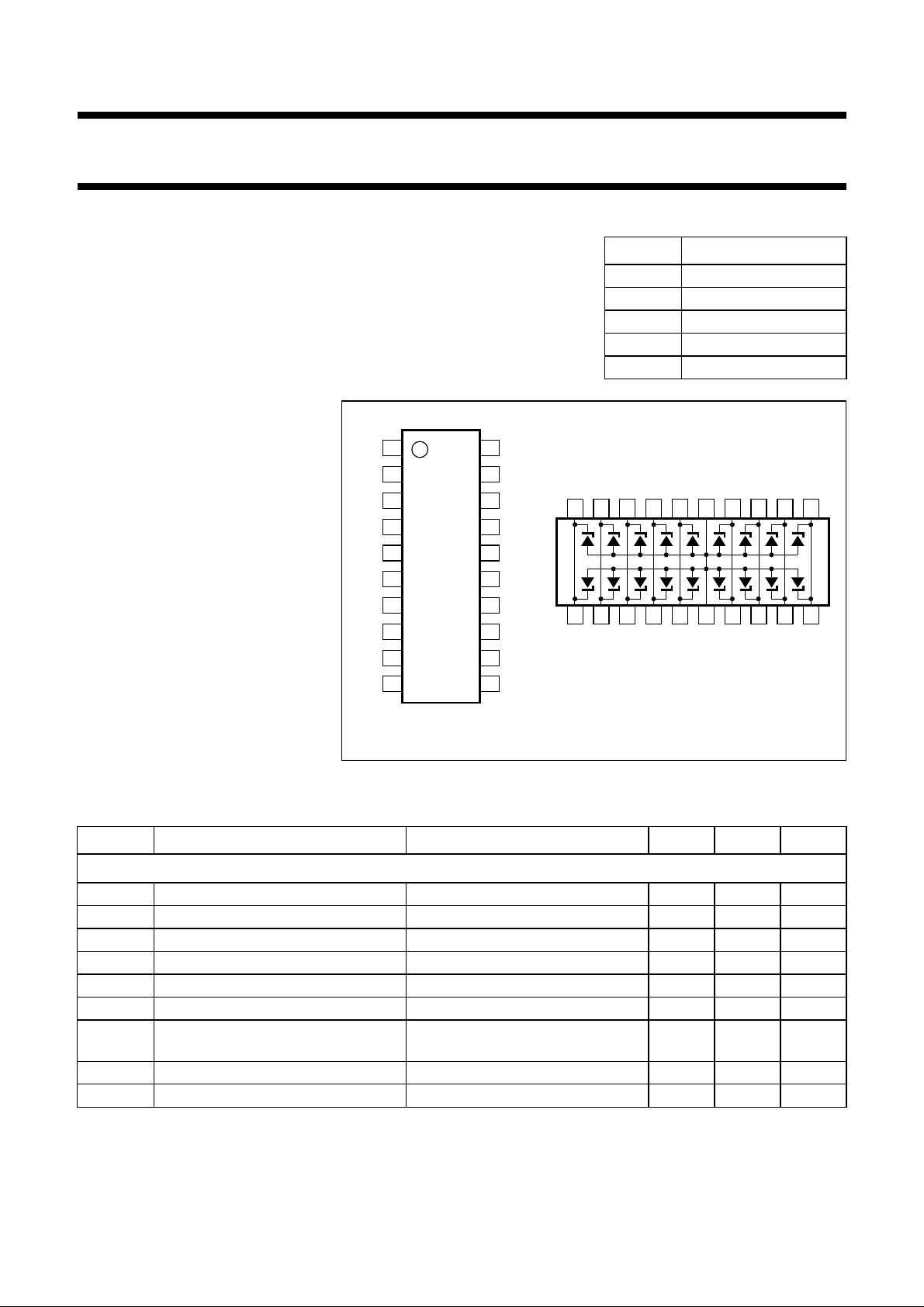
1 to 5 input (IN1 to IN5)
6 and 15 common anode (GND)
7 to 10 input (IN6 to IN9)
11 to 14 output (OUT9 to OUT6)
16 to 20 output (OUT5 to OUT1)
19 18 17 16 15 14 13 12 1120
2 3 4 5 6 7 8 9 101
MBK268
Fig.1 Pin configuration for SSOP20 (SOT339-1) and symbol.
LIMITING VALUES
In accordance with the Absolute Maximum Rating System (IEC 134).
SYMBOL PARAMETER CONDITIONS MIN. MAX. UNIT
Per diode
I
Z
I
F
I
FT
I
FSM
I
ZSM
P
P
tot
ZSM
working current T
continuous forward current T
feed-through current T
non-repetitive peak forward current tp= 1 ms; square pulse − 4.5 A
non-repetitive peak reverse current tp= 1 ms; square pulse; see Fig.2 − 2.5 A
total power dissipation T
non-repetitive peak reverse power
=25°C − 20 mA
amb
=25°C − 100 mA
amb
=25°C; note 1 − 100 mA
amb
≤ 25 °C; note 2; see Fig.3 − 0.95 W
amb
tp= 1 ms; square pulse; see Fig.4 − 25 W
dissipation
T
stg
T
j
storage temperature −65 +150 °C
operating junction temperature −65 +150 °C
Notes
1. Current is flowing from input to corresponding output.
2. One or more diodes loaded.
1998 Nov 26 2

Philips Semiconductors Product specification
9-fold ESD transient voltage suppressor BZA109TS
THERMAL CHARACTERISTICS
SYMBOL PARAMETER CONDITIONS VALUE UNIT
R
th j-a
ELECTRICAL CHARACTERISTICS
=25°C unless otherwise specified.
T
j
SYMBOL PARAMETER CONDITIONS MIN. TYP. MAX. UNIT
Per diode
V
Z
V
F
V
ZSM
I
H
r
dif
S
Z
C
d
thermal resistance from junction to ambient one or more diodes loaded 135 K/W
working voltage IZ = 250 µA 6.4 6.8 7.2 V
forward voltage IF= 100 mA −−1.1 V
non-repetitive peak reverse voltage I
= 2.5 A; tp=1ms −−10 V
ZSM
input high current VIN= 5.25 V −−0.5 µA
differential resistance IZ= 250 µA −−100 Ω
temperature coefficient of
IZ=5mA − 3 − mV/K
working voltage
diode capacitance see Fig.5
V
= 0; f = 1 MHz −−200 pF
R
V
= 5.25 V; f = 1 MHz −−100 pF
R
1998 Nov 26 3

Philips Semiconductors Product specification
9-fold ESD transient voltage suppressor BZA109TS
GRAPHICAL DATA
10
handbook, halfpage
I
ZSM
(A)
1
−1
10
110
t
(ms)
p
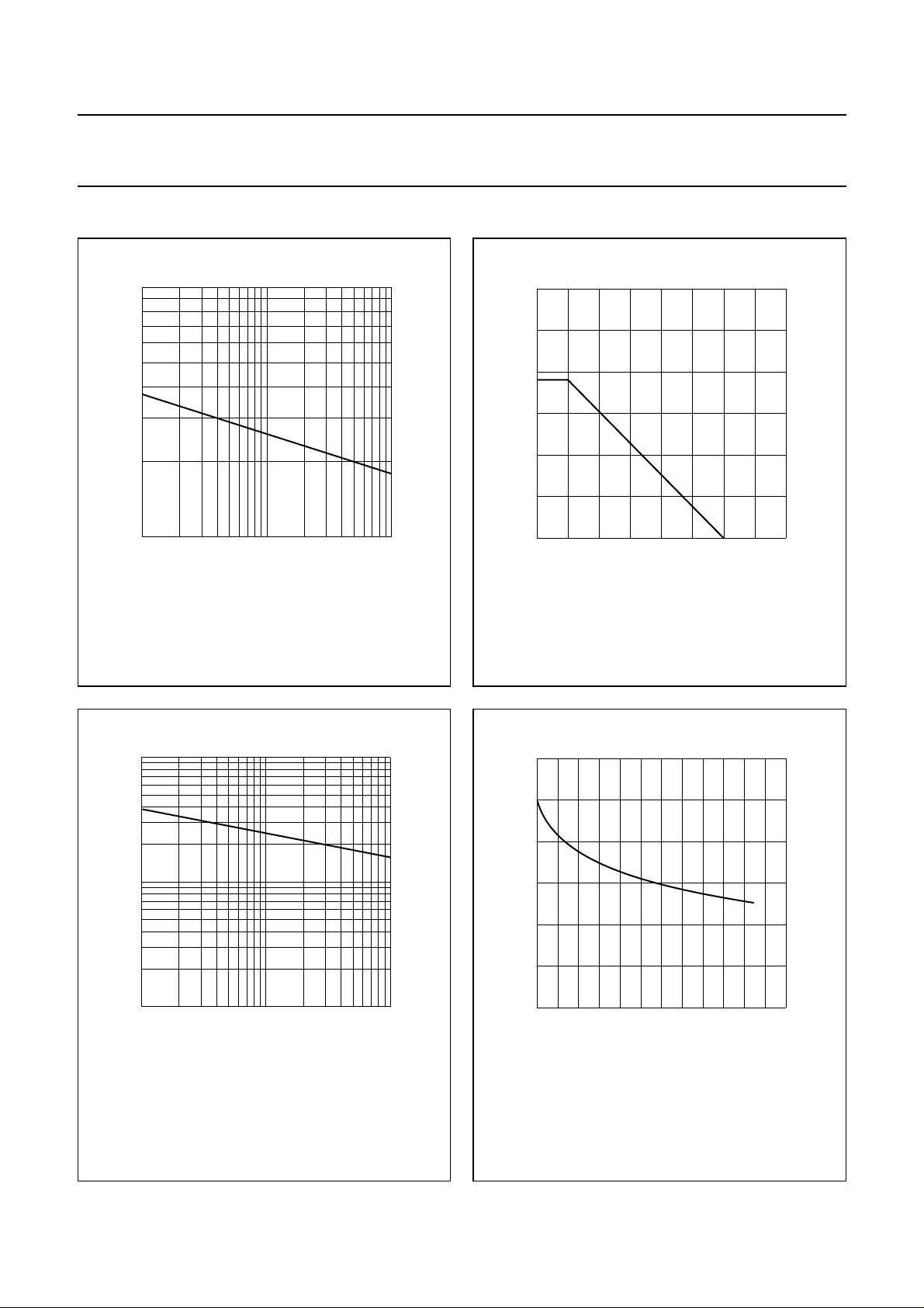
Fig.2 Maximum non-repetitive peak reverse
current as a function of pulse time.
MBK269
1.5
handbook, halfpage
P
tot
(W)
1
0.5
0
0 50 100 200
One or more diodes loaded.
Fig.3 Power derating curve.
150
T
amb
MGM148
(°C)
2
10
handbook, halfpage
P
ZSM
(W)
10
1
−1
10
P
ZSM=VZSM
V
ZSM
× I
.
is the non-repetitive peak reverse voltage at I
ZSM
110
MGM149
t
(ms)
p
.
ZSM
Fig.4 Maximum non-repetitive peak reverse power
dissipation as a function of pulse duration
(square pulse).
150
handbook, halfpage
C
d
(pF)
100
50
0
0
Tj=25°C; f = 1 MHz.
Fig.5 Diode capacitance as a function of
MBK272
26
4
V
(V)
R
reverse voltage; typical values.
1998 Nov 26 4
 Loading...