

Philips byv79eb DATASHEETS
Philips Semiconductors Product specification
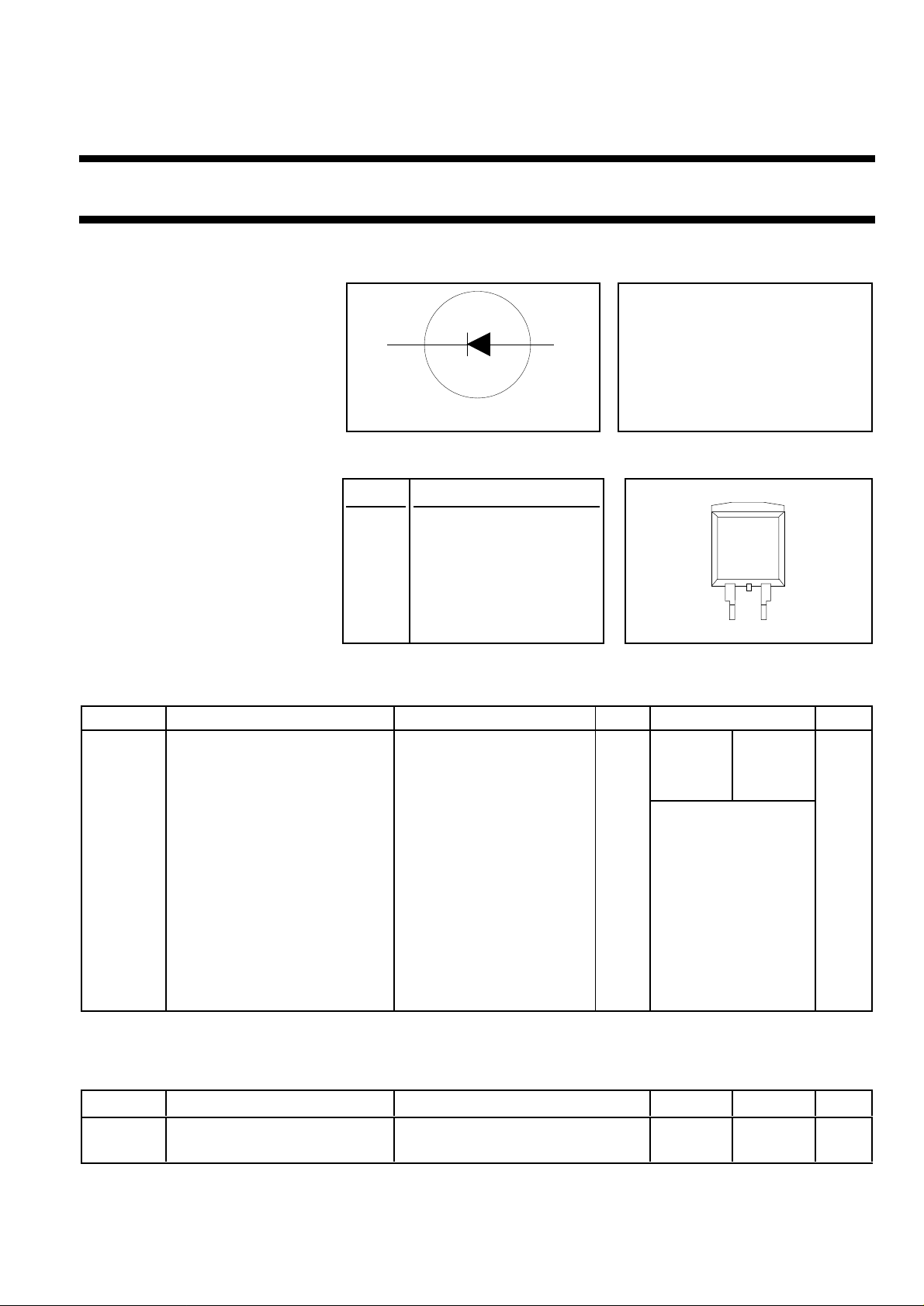
Rectifier diodes BYV79EB series
ultrafast, rugged
FEATURES SYMBOL QUICK REFERENCE DATA
• Low forward volt drop VR = 150 V/ 200 V
• Fast switching
• Soft recovery characteristic VF ≤ 0.9 V
• Reverse surge capability
• High thermal cycling performance I
• Low thermal resistance
GENERAL DESCRIPTION PINNING SOT404
k a
tab 3
= 14 A
F(AV)
I
= 0.2 A
RRM
trr ≤ 30 ns
Ultra-fast, epitaxial rectifier diodes PIN DESCRIPTION
tab
intended foruse as output rectifiers
in high frequency switched mode 1 no connection
power supplies.
2 cathode
1
The BYV79EB series issupplied in
the surface mounting SOT404 3 anode
package.
2
tab cathode
13
LIMITING VALUES
Limiting values in accordance with the Absolute Maximum System (IEC 134).
SYMBOL PARAMETER CONDITIONS MIN. MAX. UNIT
V
V
V
I
F(AV)
I
FRM
RRM
RWM
R
Peak repetitive reverse voltage - 150 200 V
Crest working reverse voltage - 150 200 V
Continuous reverse voltage Tmb ≤ 145˚C - 150 200 V
Average rectified forward square wave - 14 A
current
2
δ = 0.5; Tmb ≤ 120 ˚C
Repetitive peak forward current t = 25 µs; δ = 0.5; - 28 A
per diode Tmb ≤ 120 ˚C
I
FSM
Non-repetitive peak forward t = 10 ms - 150 A
current t = 8.3 ms - 160 A
sinusoidal; with reapplied
V
I
RRM
I
RSM
T
T
stg
j
Repetitive peak reverse current tp = 2 µs; δ = 0.001 - 0.2 A
Non-repetitive peak reverse tp = 100 µs - 0.2 A
current
Storage temperature -40 150 ˚C
Operating junction temperature - 150 ˚C
RRM(max)
1. It is not possible to make connection to pin 2 of the SOT404 package
2. Neglecting switching and reverse current losses.
BYV79EB -150 -200
ESD LIMITING VALUE
SYMBOL PARAMETER CONDITIONS MIN. MAX. UNIT
V
C
July 1998 1 Rev 1.100
Electrostatic discharge Human body model; - 8 kV
capacitor voltage C = 250 pF; R = 1.5 kΩ

Philips Semiconductors Product specification
Rectifier diodes BYV79EB series
ultrafast, rugged
THERMAL RESISTANCES
SYMBOL PARAMETER CONDITIONS MIN. TYP. MAX. UNIT
R
th j-mb
R
th j-a
ELECTRICAL CHARACTERISTICS
Tj = 25 ˚C unless otherwise stated
SYMBOL PARAMETER CONDITIONS MIN. TYP. MAX. UNIT
V
F
I
R
Q
s
t
rr1
t
rr2
V
fr
Thermal resistance junction to - - 2 K/W
mounting base
Thermal resistance junction to minimum footprint, FR4 board - 50 - K/W
ambient
Forward voltage IF = 14 A; Tj = 150˚C - 0.83 0.90 V
IF = 14 A - 0.95 1.05 V
IF = 50 A - 1.2 1.4 V
Reverse current VR = V
VR = V
; Tj = 100 ˚C - 0.5 1.3 mA
RRM
RRM
-550µA
Reverse recovery charge IF = 2 A; VR ≥ 30 V; -dIF/dt = 20 A/µs- 6 15 nC
Reverse recovery time IF = 1 A; VR ≥ 30 V; - 20 30 ns
-dIF/dt = 100 A/µs
Reverse recovery time IF = 0.5 A to IR = 1 A; I
Forward recovery voltage IF = 1 A; dIF/dt = 10 A/µs-1-V
= 0.25 A - 13 22 ns
rec
July 1998 2 Rev 1.100
Philips Semiconductors Product specification
Rectifier diodes BYV79EB series
ultrafast, rugged
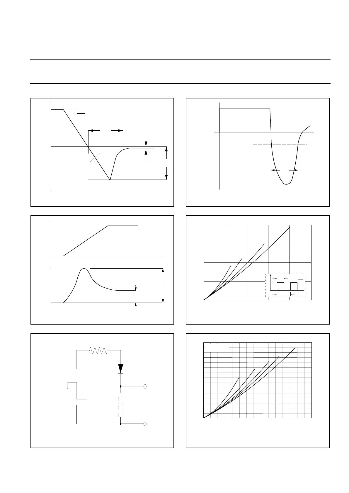
I
F
dI
F
dt
t
rr
time
Q
s
I
R
I
F
I
rrm
Fig.1. Definition of t
, Qs and I
rr1
10%
100%
rrm
time
V
F
V
fr
V
F
time
Fig.2. Definition of V
fr
0.5A
IF
0A
I = 0.25A
rec
IR
trr2
I = 1A
R
Fig.4. Definition of t
PF / W
20
Vo = 0.744 V
Rs = 0.0112 Ohms
15
10
5
0
0 5 10 15 20 25
0.1
BYV79
0.5
0.2
IF(AV) / A
rr2
Tmb(max) / C
D = 1.0
p
p
t
I
t
D =
T
T
t
Fig.5. Maximum forward dissipation PF = f(I
square current waveform where I
F(AV)
=I
F(RMS)
110
120
130
140
150
);
F(AV)
x √D.
1.9
F(AV)
Tmb(max) / C
a = 1.57
.
120
130
140
150
F(AV)
);
R
Voltage Pulse Source
Current
shunt
Fig.3. Circuit schematic for t
D.U.T.
to ’scope
rr2
PF / W
15
Vo = 0.744 V
Rs = 0.0112 Ohms
10
5
0
0 5 10 15
BYV79
2.2
2.8
4
IF(AV) / A
Fig.6. Maximum forward dissipation PF = f(I
sinusoidal current waveform where a = form
factor = I
F(RMS)
/ I
July 1998 3 Rev 1.100
 Loading...