

Philips byv74f DATASHEETS
Philips Semiconductors Product specification
Dual rectifier diodes BYV74F series
ultrafast
FEATURES SYMBOL QUICK REFERENCE DATA
• Low forward volt drop V
• Fast switching
• Soft recovery characteristic V
• High thermal cycling performance
a1
13
a2
• Isolated mounting tab I
k
2
= 300 V/ 400 V/ 500 V
R
≤ 1.12 V
F
= 20 A
O(AV)
trr ≤ 60 ns
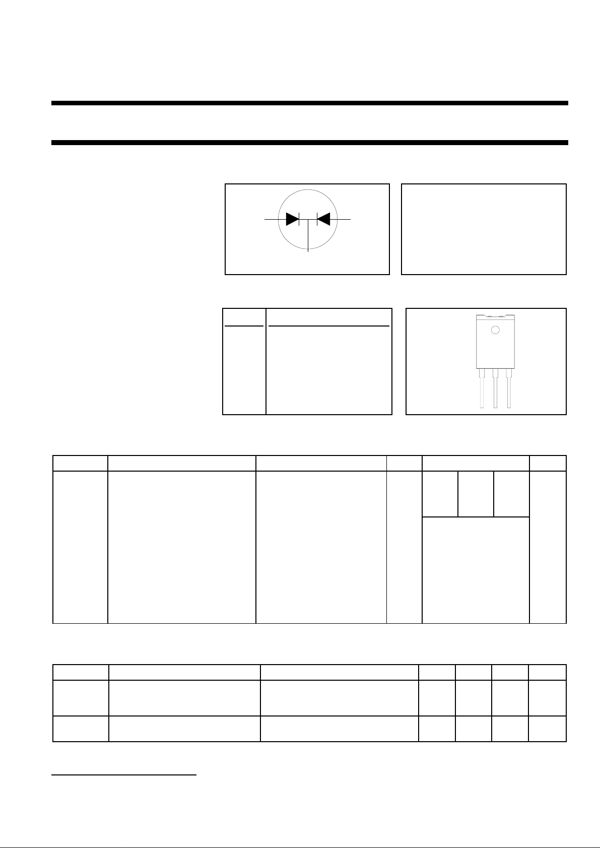
GENERAL DESCRIPTION PINNING SOT199
Dual, common cathode, ultra-fast, PIN DESCRIPTION
epitaxial rectifier diodes intended
for use as output rectifiers in high 1 anode 1
case
frequency switched mode power
supplies. 2 cathode
The BYV74F series is supplied in 3 anode 2
the conventional leaded SOT199
package. tab isolated
12
3
LIMITING VALUES
Limiting values in accordance with the Absolute Maximum System (IEC 134).
SYMBOL PARAMETER CONDITIONS MIN. MAX. UNIT
V
V
V
I
O(AV)
I
FRM
I
FSM
T
T
RRM
RWM
R
stg
j
Peak repetitive reverse voltage - 300 400 500 V
Crest working reverse voltage - 300 400 500 V
Continuous reverse voltage Tmb ≤ 117˚C - 300 400 500 V
Average rectified output current square wave; δ = 0.5; - 20 A
(both diodes conducting)
1
Ths ≤ 54 ˚C
Repetitive peak forward current t = 25 µs; δ = 0.5; - 30 A
per diode Ths ≤ 54 ˚C
Non-repetitive peak forward t = 10 ms - 150 A
current per diode. t = 8.3 ms - 160 A
sinusoidal; with reapplied
V
RRM(max)
Storage temperature -40 150 ˚C
Operating junction temperature - 150 ˚C
BYV74F -300 -400 -500
ISOLATION LIMITING VALUE & CHARACTERISTIC
Ths = 25 ˚C unless otherwise specified
SYMBOL PARAMETER CONDITIONS MIN. TYP. MAX. UNIT
V
isol
C
isol
1 Neglecting switching and reverse current losses.
September 1998 1 Rev 1.300
Repetitive peak voltage from all R.H. ≤ 65 % ; clean and dustfree - - 2500 V
three terminals to external
heatsink
Capacitance from T2 to external f = 1 MHz - 22 - pF
heatsink

Philips Semiconductors Product specification
Dual rectifier diodes BYV74F series
ultrafast
THERMAL RESISTANCES
SYMBOL PARAMETER CONDITIONS MIN. TYP. MAX. UNIT
R
th j-hs
R
th j-a
ELECTRICAL CHARACTERISTICS
characteristics are per diode at Tj = 25 ˚C unless otherwise stated
SYMBOL PARAMETER CONDITIONS MIN. TYP. MAX. UNIT
V
F
I
R
Q
s
t
rr
I
rrm
V
fr
Thermal resistance junction to both diodes conducting
heatsink with heatsink compound - - 4.0 K/W
without heatsink compound - - 8.0 K/W
per diode
with heatsink compound - - 5.0 K/W
without heatsink compound - - 9.0 K/W
Thermal resistance junction to in free air. - 35 - K/W
ambient
Forward voltage IF = 15 A; Tj = 150˚C - 0.95 1.12 V
IF = 15 A - 1.08 1.25 V
IF = 30 A - 1.15 1.36 V
Reverse current VR = V
Reverse recovery charge IF = 2 A to VR ≥ 30 V; - 40 60 nC
VR = V
RRM
; Tj = 100 ˚C - 0.3 0.8 mA
RRM
-1050µA
dIF/dt = 20 A/µs
Reverse recovery time IF = 1 A to VR ≥ 30 V; - 50 60 ns
dIF/dt = 100 A/µs
Peak reverse recovery current IF = 10 A to VR ≥ 30 V; - 4.2 5.2 A
dIF/dt = 50 A/µs; Tj = 100˚C
Forward recovery voltage IF = 10 A; dIF/dt = 10 A/µs - 2.5 - V
September 1998 2 Rev 1.300
 Loading...