

Philips BYV72EW-200, BYV72EW-150 Datasheet
Philips Semiconductors Product specification
Rectifier diodes BYV72EW series
ultrafast, rugged
FEATURES SYMBOL QUICK REFERENCE DATA
• Low forward volt drop VR = 150 V/ 200 V
• Fast switching
• Soft recovery characteristic VF ≤ 0.85 V
• Reverse surge capability
a1
13
• High thermal cycling performance I
• Low thermal resistance
k
2
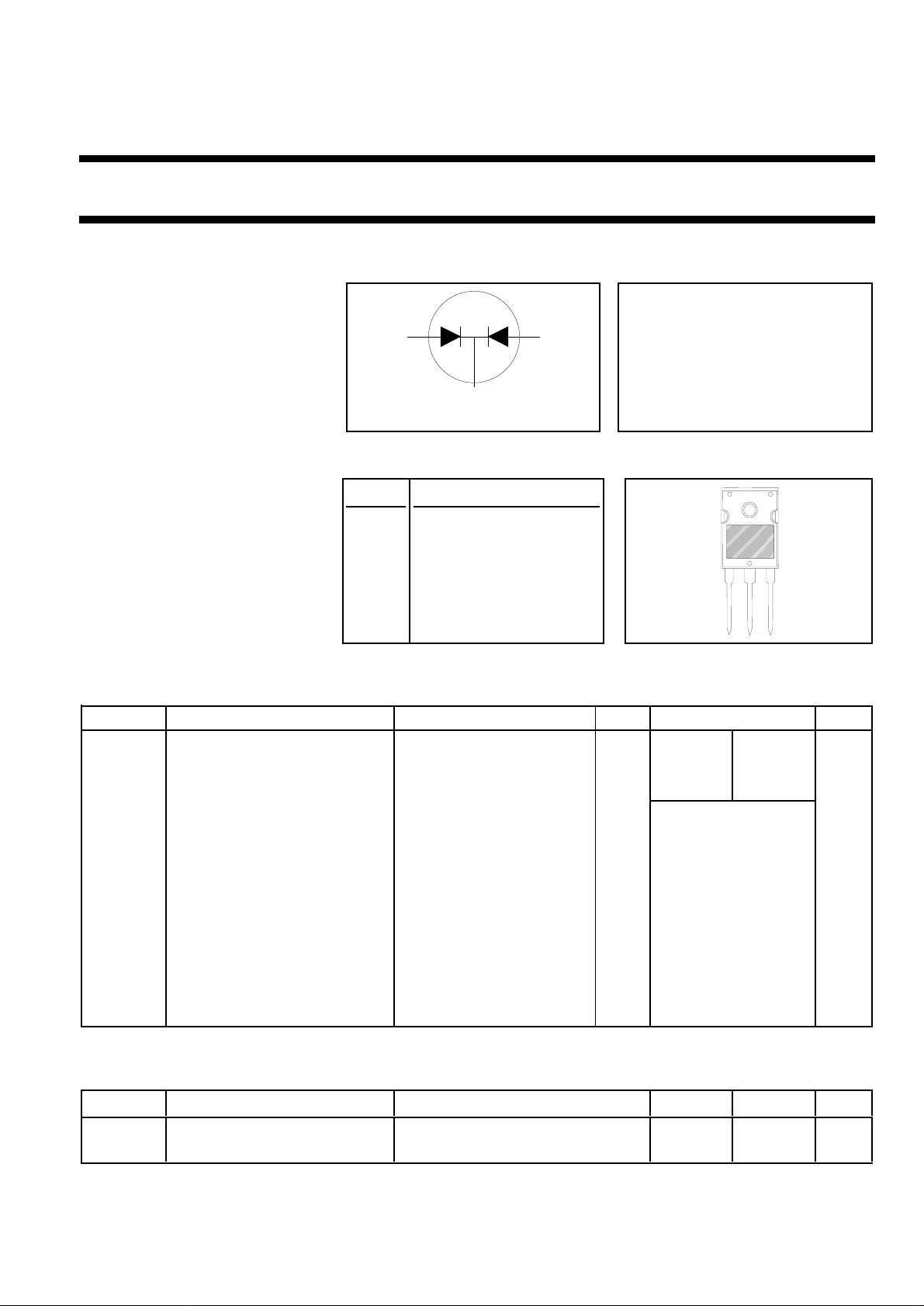
GENERAL DESCRIPTION PINNING SOT429 (TO247)
Dual, ultra-fast, epitaxial rectifier PIN DESCRIPTION
diodes intended for use as output
rectifiersinhighfrequencyswitched 1 anode 1
mode power supplies.
TheBYV72EW seriesis suppliedin
the conventional leaded SOT429 3 anode 2
(TO247) package.
2 cathode
tab cathode
a2
= 30 A
O(AV)
I
= 0.2 A
RRM
trr ≤ 28 ns
2
1
3
LIMITING VALUES
Limiting values in accordance with the Absolute Maximum System (IEC 134).
SYMBOL PARAMETER CONDITIONS MIN. MAX. UNIT
BYV72EW -150 -200
V
V
V
I
O(AV)
I
FRM
RRM
RWM
R
Peak repetitive reverse voltage - 150 200 V
Crest working reverse voltage - 150 200 V
Continuous reverse voltage Tmb ≤ 144˚C - 150 200 V
Average rectified output current square wave - 30 A
(both diodes conducting)
1
δ = 0.5; Tmb ≤ 104 ˚C
Repetitive peak forward current t = 25 µs; δ = 0.5; - 30 A
per diode Tmb ≤ 104 ˚C
I
FSM
Non-repetitive peak forward t = 10 ms - 150 A
current per diode t = 8.3 ms - 160 A
sinusoidal; with reapplied
V
I
RRM
Repetitive peak reverse current tp = 2 µs; δ = 0.001 - 0.2 A
RWM(max)
per diode
I
RSM
T
T
stg
j
Non-repetitive peak reverse tp = 100 µs - 0.2 A
current per diode
Storage temperature -40 150 ˚C
Operating junction temperature - 150 ˚C
1 Neglecting switching and reverse current losses.
ESD LIMITING VALUE
SYMBOL PARAMETER CONDITIONS MIN. MAX. UNIT
V
C
Electrostatic discharge Human body model; - 8 kV
capacitor voltage C = 250 pF; R = 1.5 kΩ
October 1998 1 Rev 1.200

Philips Semiconductors Product specification
Rectifier diodes BYV72EW series
ultrafast, rugged
THERMAL RESISTANCES
SYMBOL PARAMETER CONDITIONS MIN. TYP. MAX. UNIT
R
th j-mb
R
th j-a
ELECTRICAL CHARACTERISTICS
characteristics are per diode at Tj = 25 ˚C unless otherwise stated
SYMBOL PARAMETER CONDITIONS MIN. TYP. MAX. UNIT
V
F
I
R
Q
s
t
rr1
t
rr2
V
fr
Thermal resistance junction to per diode - - 2.4 K/W
mounting base both diodes conducting - - 1.4 K/W
Thermal resistance junction to in free air - 45 - K/W
ambient
Forward voltage IF = 15 A; Tj = 150˚C - 0.83 0.90 V
IF = 15 A - 0.95 1.05 V
IF = 30 A - 1.00 1.20 V
Reverse current VR = V
VR = V
; Tj = 100 ˚C - 0.5 1 mA
RWM
RWM
- 10 100 µA
Reverse recovery charge IF = 2 A; VR ≥ 30 V; -dIF/dt = 20 A/µs- 6 15 nC
Reverse recovery time IF = 1 A; VR ≥ 30 V; - 20 28 ns
-dIF/dt = 100 A/µs
Reverse recovery time IF = 0.5 A to IR = 1 A; I
Forward recovery voltage IF = 1 A; dIF/dt = 10 A/µs-1-V
= 0.25 A - 13 22 ns
rec
October 1998 2 Rev 1.200
 Loading...