

Philips BYR29-800, BYR29-700, BYR29-600, BYR29-500 Datasheet

Philips Semiconductors Product specification
Rectifier diodes BYR29 series
ultrafast
FEATURES SYMBOL QUICK REFERENCE DATA
• Low forward volt drop V
= 500 V/ 600 V/ 700 V /
R
• Fast switching 800 V
• Soft recovery characteristic
• Reverse surge capability V
k a
12
≤ 1.5 V
F
• High thermal cycling performance
• Low thermal resistance I
F(AV)
= 8 A
trr ≤ 75 ns
GENERAL DESCRIPTION PINNING SOD59 (TO220AC)
Ultra-fast, epitaxial rectifier diodes PIN DESCRIPTION
intended foruse as output rectifiers
in high frequency switched mode 1 cathode
power supplies.
2 anode
TheBYR29series issupplied in the
conventional leaded SOD59 tab cathode
(TO220AC) package.
tab
1
2
LIMITING VALUES
Limiting values in accordance with the Absolute Maximum System (IEC 134).
SYMBOL PARAMETER CONDITIONS MIN. MAX. UNIT
V
V
V
I
F(AV)
I
FRM
I
FSM
T
T
RRM
RWM
R
stg
j
Peak repetitive reverse voltage - 500 600 700 800 V
Crest working reverse voltage - 500 600 700 800 V
Continuous reverse voltage - 500 600 700 800 V
Average forward current
1
square wave; - 8 A
δ = 0.5;
Tmb ≤ 115 ˚C
Repetitive peak forward current t = 25 µs; δ = 0.5; - 16 A
Tmb ≤ 115 ˚C
Non-repetitive peak forward t = 10 ms - 60 A
current t = 8.3 ms - 66 A
sinusoidal; with
reapplied V
Storage temperature -40 150 ˚C
Operating junction temperature - 150 ˚C
BYR29 -500 -600 -700 -800
RRM(max)
THERMAL RESISTANCES
SYMBOL PARAMETER CONDITIONS MIN. TYP. MAX. UNIT
R
th j-mb
R
th j-a
1 Neglecting switching and reverse current losses
September 1998 1 Rev 1.300
Thermal resistance junction to - - 2.5 K/W
mounting base
Thermal resistance junction to in free air. - 60 - K/W
ambient
Philips Semiconductors Product specification
Rectifier diodes BYR29 series
ultrafast
ELECTRICAL CHARACTERISTICS
Tj = 25 ˚C unless otherwise stated
SYMBOL PARAMETER CONDITIONS MIN. TYP. MAX. UNIT
V
F
I
R
Q
s
t
rr
I
rrm
V
fr
Forward voltage IF = 8 A; Tj = 150˚C - 1.07 1.50 V
IF = 20 A - 1.75 1.95 V
Reverse current VR = V
Reverse recovery charge IF = 2 A to VR ≥ 30 V; - 150 200 nC
VR = V
RRM
; Tj = 100 ˚C - 0.1 0.2 mA
RRM
- 1.0 10 µA
dIF/dt = 20 A/µs
Reverse recovery time IF = 1 A to VR ≥ 30 V; - 60 75 ns
dIF/dt = 100 A/µs
Peak reverse recovery current IF = 10 A to VR ≥ 30 V; - - 6 A
dIF/dt = 50 A/µs; Tj = 100 ˚C
Forward recovery voltage IF = 10 A; dIF/dt = 10 A/µs - 5.0 - V
0.5
=I
2.2
Tmb(max) / C
t
p
T
F(RMS)
Tmb(max) / C
1.9
D = 1.0
t
p
D =
T
t
x √D.
a = 1.57
100
112.5
125
137.5
150
F(AV)
120
130
140
150
F(AV)
);
);
PF / W
I
F
dI
F
dt
t
rr
time
Q
s
I
R
I
rrm
10%
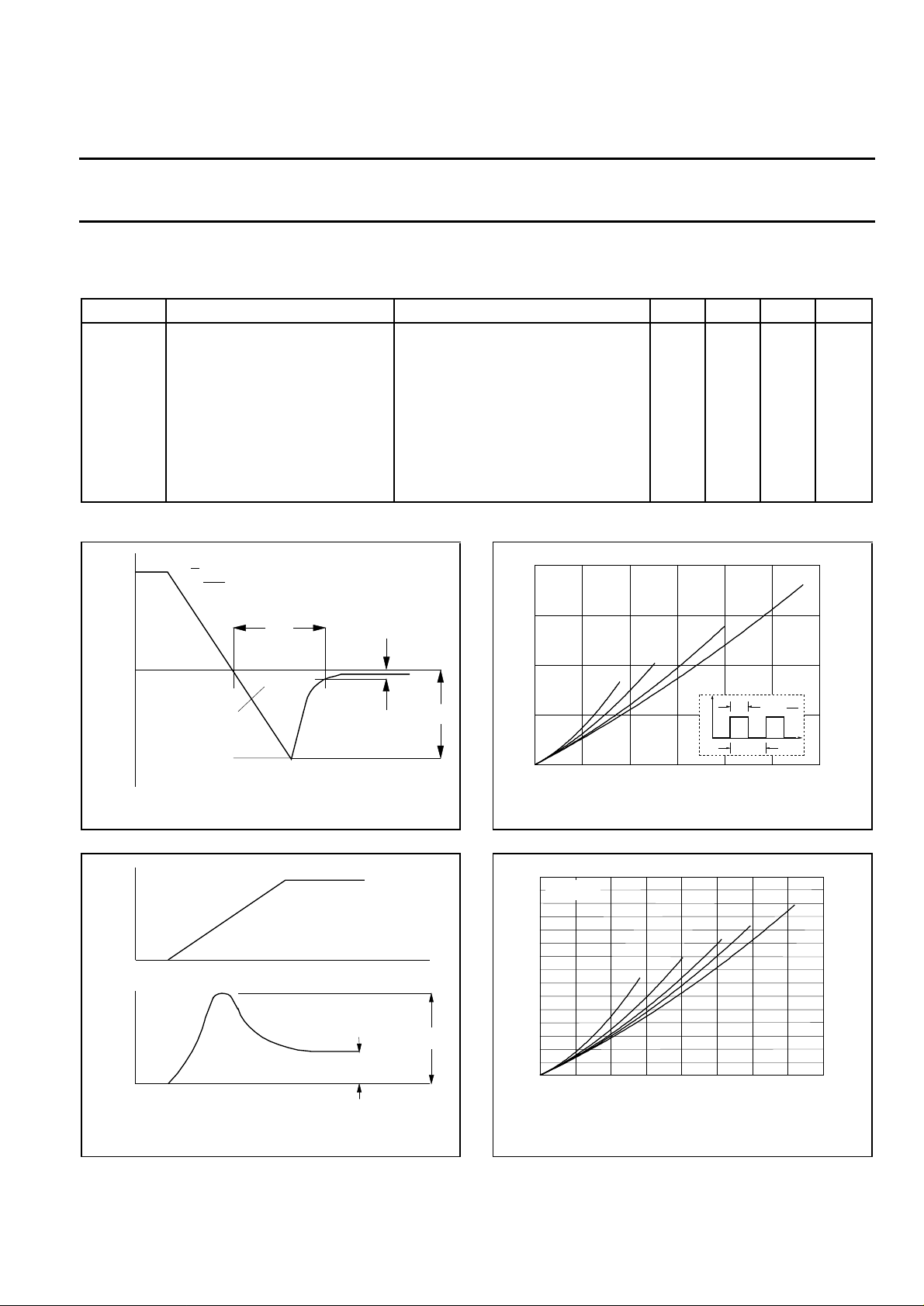
Fig.1. Definition of trr, Qs and I
100%
rrm
20
Vo = 1.26 V
Rs = 0.03 Ohms
15
10
5
0
024681012
0.1
Fig.3. Maximum forward dissipation PF = f(I
square wave where I
I
F
time
V
F
V
fr
V
F
time
Fig.2. Definition of V
fr
PF / W
15
Vo = 1.26 V
Rs = 0.03 Ohms
10
5
0
012345678
Fig.4. Maximum forward dissipation PF = f(I
BYR29
0.2
I
IF(AV) / A
F(AV)
BYR29
2.8
4
IF(AV) / A
sinusoidal current waveform where a = form
factor = I
F(RMS)
/ I
F(AV)
.
September 1998 2 Rev 1.300
 Loading...