

Philips BYQ63 Datasheet

DISCRETE SEMICONDUCTORS
DATA SH EET
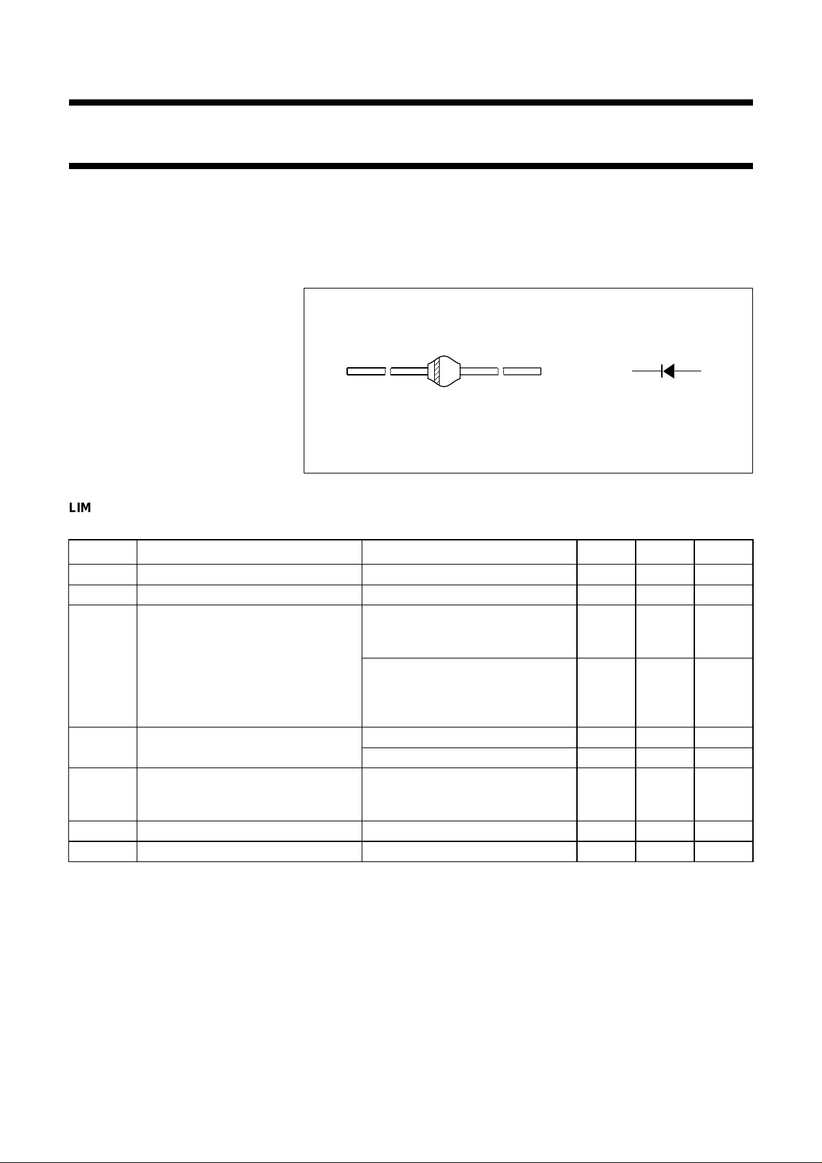
handbook, 2 columns
M3D116
BYQ63
Ripple blocking diode
Product specification
1998 Dec 04
Philips Semiconductors Product specification
Ripple blocking diode BYQ63
FEATURES
• Glass passivated
• High maximum operating
temperature
DESCRIPTION
Rugged glass SOD57 package, using
a high temperature alloyed
construction.
The SOD57 is hermetically sealed
and fatigue free as coefficients of
expansion of all used parts are
matched.
• Low leakage current
• Excellent stability
• Guaranteed minimum turn-on time
for absorbing forward current
transients and oscillations
ka
2/3 page (Datasheet)
• Specially designed as rectifier in
the auxiliary power supply in e.g.
MAM047
switched mode power supplies
• Available in ammo-pack
• Also available with preformed leads
Fig.1 Simplified outline (SOD57) and symbol.
for easy insertion.
LIMITING VALUES
In accordance with the Absolute Maximum Rating System (IEC 134).
SYMBOL PARAMETER CONDITIONS MIN. MAX. UNIT
V
RRM
V
R
I
F(AV)
repetitive peak reverse voltage − 300 V
continuous reverse voltage − 300 V
average forward current averaged over any 20 ms period;
− 1.05 A
Ttp=85°C; lead length = 10 mm;
see Fig.2; see also Fig.4
averaged over any 20 ms period;
T
=60°C;
amb
− 0.68 A
PCB mounting (Fig.8);
see Fig.3; see also Fig.4
I
FRM
I
FSM
T
T
stg
j
repetitive peak forward current Ttp=85°C − 9.6 A
T
=60°C − 6.4 A
amb
non-repetitive peak forward current t = 10 ms half sine wave;
Tj=T
VR=V
prior to surge;
j max
RRMmax
− 30 A
storage temperature −65 +175 °C
junction temperature −65 +175 °C
1998 Dec 04 2
Philips Semiconductors Product specification
Ripple blocking diode BYQ63
ELECTRICAL CHARACTERISTICS
T
=25°C unless otherwise specified.
j
SYMBOL PARAMETER CONDITIONS MIN. TYP. MAX. UNIT
V
F
I
R
forward voltage IF= 1 A; Tj=T
I
= 1 A; see Fig.5 −−2.15 V
F
reverse current VR=V
RRMmax
see Fig.6
V
R=VRRMmax
see Fig.6
t
fr
forward recovery time when switched to IF=5A
in 50 ns; see Fig.9
t
on
turn-on time when switched from VF= 0 to
VF= 3 V; measured between
10% and 90% of I
see Fig.11
t
rr
reverse recovery time when switched from IF= 0.5 A to
IR= 1 A; measured at
IR= 0.25 A; see Fig.11
C
d
diode capacitance f = 1 MHz; VR= 0; see Fig.7 − 35 − pF
; see Fig.5 −−1.3 V
j max
;
; Tj= 165 °C;
−−5µA
−−150 µA
−−1.5 µs
400 −−ns
;
Fmax
−−150 ns
THERMAL CHARACTERISTICS
SYMBOL PARAMETER CONDITIONS VALUE UNIT
R
R
th j-tp
th j-a
thermal resistance from junction to tie-point lead length = 10 mm 46 K/W
thermal resistance from junction to ambient note 1 100 K/W
Note
1. Device mounted on an epoxy-glass printed-circuit board, 1.5 mm thick; thickness of Cu-layer ≥40 µm, see Fig.8.
For more information please refer to the
‘General Part of associated Handbook.’
1998 Dec 04 3
 Loading...