

Philips BYQ30E-200, BYQ30ED-150, BYQ30ED-100, BYQ30EB-100 Datasheet
Philips Semiconductors Product specification
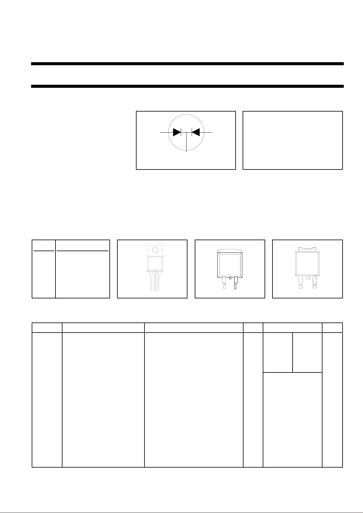
Rectifier diodes BYQ30E, BYQ30EB, BYQ30ED series
ultrafast, rugged
FEATURES SYMBOL QUICK REFERENCE DATA
• Low forward volt drop VR = 150 V/ 200 V
• Fast switching
• Soft recovery characteristic VF ≤ 0.95 V
• Reverse surge capability
a1
13
• High thermal cycling performance I
• Low thermal resistance
k
2
GENERAL DESCRIPTION
Dual, ultra-fast, epitaxial rectifier diodes intended for use as output rectifiers in high frequency switched mode power
supplies.
The BYQ30E series is supplied in the SOT78 conventional leaded package.
The BYQ30EB series is supplied in the SOT404 surface mounting package.
The BYQ30ED series is supplied in the SOT428 surface mounting package.
a2
= 16 A
O(AV)
I
= 0.2 A
RRM
trr ≤ 25 ns
PINNING SOT78 (TO220AB) SOT404 SOT428
PIN DESCRIPTION
1 anode 1
2 cathode
1
3 anode 2
tab cathode
tab
123
tab
2
13
tab
123
LIMITING VALUES
Limiting values in accordance with the Absolute Maximum System (IEC 134)
SYMBOL PARAMETER CONDITIONS MIN. MAX. UNIT
BYQ30E/ BYQ30EB/ BYQ30ED -150 -200
V
RRM
V
RWM
V
R
I
O(AV)
I
FRM
I
FSM
I
RRM
I
RSM
T
j
T
stg
1. It is not possible to make connection to pin 2 of the SOT428 or SOT404 packages.
Peak repetitive reverse - 150 200 V
voltage
Working peak reverse - 150 200 V
voltage
Continuous reverse voltage - 150 200 V
Average rectified output square wave; δ = 0.5; Tmb ≤ 104 ˚C - 16 A
current (both diodes
conducting)
Repetitive peak forward square wave; δ = 0.5; Tmb ≤ 104 ˚C - 16 A
current per diode
Non-repetitive peak forward t = 10 ms - 80 A
current per diode t = 8.3 ms - 88 A
sinusoidal; with reapplied V
RRM(max)
Peak repetitive reverse tp = 2 µs; δ = 0.001 - 0.2 A
surge current per diode
Peak non-repetitive reverse tp = 100 µs - 0.2 A
surge current per diode
Operating junction - 150 ˚C
temperature
Storage temperature - 40 150 ˚C
October 1998 1 Rev 1.200

Philips Semiconductors Product specification
Rectifier diodes BYQ30E, BYQ30EB, BYQ30ED series
ultrafast, rugged
ESD LIMITING VALUE
SYMBOL PARAMETER CONDITIONS MIN. MAX. UNIT
V
C
Electrostatic discharge Human body model; - 8 kV
capacitor voltage C = 250 pF; R = 1.5 kΩ
THERMAL RESISTANCES
SYMBOL PARAMETER CONDITIONS MIN. TYP. MAX. UNIT
R
R
th j-mb
th j-a
Thermal resistance junction per diode - - 3 K/W
to mounting base both diodes - - 2.5 K/W
Thermal resistance junction SOT78 package, in free air - 60 - K/W
to ambient SOT404 and SOT428 packages, pcb - 50 - K/W
mounted, minimum footprint, FR4 board
ELECTRICAL CHARACTERISTICS
All characteristics are per diode at Tj = 25 ˚C unless otherwise specified
SYMBOL PARAMETER CONDITIONS MIN. TYP. MAX. UNIT
V
F
I
R
Q
rr
t
rr1
t
rr2
V
fr
Forward voltage IF = 8 A; Tj = 150˚C - 0.84 0.95 V
IF = 16 A; Tj = 150˚C - 1 1.15 V
IF = 16 A - 1.12 1.25 V
Reverse current VR = V
VR = V
RWM
; Tj = 100˚C - 0.3 0.6 mA
RWM
-430µA
Reverse recovered charge IF = 2 A; VR ≥ 30 V; -dIF/dt = 20 A/µs-411nC
Reverse recovery time IF = 1 A; VR ≥ 30 V; -dIF/dt = 100 A/µs2025ns
Reverse recovery time IF = 0.5 A to IR = 1 A; I
= 0.25 A - 12 22 ns
rec
Forward recovery voltage IF = 1 A; dIF/dt = 10 A/µs-1-V
October 1998 2 Rev 1.200
Philips Semiconductors Product specification
Rectifier diodes BYQ30E, BYQ30EB, BYQ30ED series
ultrafast, rugged
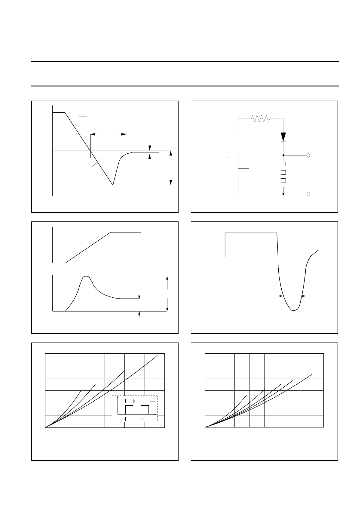
R
I = 1A
R
Current
shunt
D.U.T.
to ’scope
rr2
trr2
rr2
I
rrm
dI
F
dt
t
rr
time
Q
s
, Qs and I
rr1
10%
rrm
100%
time
V
fr
V
F
Voltage Pulse Source
Fig.4. Circuit schematic for t
0.5A
IF
0A
I = 0.25A
rec
IR
I
F
I
R
Fig.1. Definition of t
I
F
V
F
time
Fig.2. Definition of V
fr
Fig.5. Definition of t
Forward dissipation, PF (W)
12
Vo = 0.75 V
Rs = 0.025 Ohms
10
8
6
4
2
0
024681012
0.1
Average forward current, IF(AV) (A)
Fig.3. Maximum forward dissipation PF = f(I
diode; square current waveform where
I
F(AV)
=I
BYQ30
0.2
F(RMS)
I
x √D.
Tmb(max) / C
D = 1.0
0.5
t
p
T
D =
p
t
T
t
F(AV)
) per
114
120
126
132
138
144
150
Forward dissipation, PF (W)
12
Vo = 0.75 V
Rs 0.025 Ohms
10
8
6
4
2
0
012345678
4
Average forward current, IF(AV) (A)
Fig.6. Maximum forward dissipation PF = f(I
diode; sinusoidal current waveform where a = form
factor = I
BYQ30
2.8
F(RMS)
/ I
2.2
F(AV)
Tmb(max) / C
1.9
.
a = 1.57
F(AV)
114
120
126
132
138
144
150
) per
October 1998 3 Rev 1.200
 Loading...