

Philips BYG80E, BYG80B, BYG80J, BYG80G Datasheet
DATA SH EET
Product specification
Supersedes data of 1996 May 24
1997 Nov 25
DISCRETE SEMICONDUCTORS
BYG80 series
Ultra fast low-loss
controlled avalanche rectifiers
k, halfpage
M3D168

1997 Nov 25 2
Philips Semiconductors Product specification
Ultra fast low-loss
controlled avalanche rectifiers
BYG80 series
FEATURES
• Glass passivated
• High maximum operating
temperature
• Low leakage current
• Excellent stability
• Guaranteed avalanche energy
absorption capability
• UL 94V-O classified plastic
package
• Shipped in 12 mm embossed tape.
DESCRIPTION
DO-214AC surface mountable
package with glass passivated chip.
The well-defined void-free case is of a
transfer-moulded thermo-setting
plastic.
Fig.1 Simplified outline (DO-214AC; SOD106) and symbol.
handbook, 4 columns
MSA474
Top view Side view
cathode
band
ka
LIMITING VALUES
In accordance with the Absolute Maximum Rating System (IEC 134).
SYMBOL PARAMETER CONDITIONS MIN. MAX. UNIT
V
RRM
repetitive peak reverse voltage
BYG80A − 50 V
BYG80B − 100 V
BYG80C − 150 V
BYG80D − 200 V
BYG80F − 300 V
BYG80G − 400 V
BYG80J − 600 V
V
R
continuous reverse voltage
BYG80A − 50 V
BYG80B − 100 V
BYG80C − 150 V
BYG80D − 200 V
BYG80F − 300 V
BYG80G − 400 V
BYG80J − 600 V
I
F(AV)
average forward current Ttp= 100 °C; see Figs 2, 3 and 4
averaged over any 20 ms period;
see also Figs 17, 18 and 19
BYG80A to D − 2.4 A
BYG80F; BYG80G − 2.3 A
BYG80J − 2.0 A
I
F(AV)
average forward current T
amb
=60°C; AL2O3 PCB mounting
(see Fig.27); see Figs 5, 6 and 7
averaged over any 20 ms period;
see also Figs 17, 18 and 19
BYG80A to D − 1.25 A
BYG80F; BYG80G − 1.15 A
BYG80J − 0.95 A

1997 Nov 25 3
Philips Semiconductors Product specification
Ultra fast low-loss
controlled avalanche rectifiers
BYG80 series
ELECTRICAL CHARACTERISTICS
T
j
=25°C unless otherwise specified.
I
F(AV)
average forward current T
amb
=60°C; epoxy PCB mounting
(see Fig.27); see Figs 5, 6 and 7
averaged over any 20 ms period;
see also Figs 17, 18 and 19
BYG80A to D − 0.95 A
BYG80F; BYG80G − 0.85 A
BYG80J − 0.65 A
I
FRM
repetitive peak forward current Ttp= 100 °C; see Figs 8, 9 and 10
BYG80A to D − 21 A
BYG80F; BYG80G − 21 A
BYG80J − 18 A
I
FRM
repetitive peak forward current T
amb
=60°C; AL2O3PCB mounting;
see Figs 11, 12 and 13
BYG80A to D − 11 A
BYG80F; BYG80G − 11 A
BYG80J − 9A
I
FRM
repetitive peak forward current T
amb
=60°C; epoxy PCB mounting;
see Figs 14, 15 and 16
BYG80A to D − 8A
BYG80F; BYG80G − 8A
BYG80J − 6A
I
FSM
non-repetitive peak forward current t = 8.3 ms half sine wave; Tj=25°C
prior to surge; VR=V
RRMmax
BYG80A to D − 36 A
BYG80F; BYG80G; BYG80J − 32 A
E
RSM
non-repetitive peak reverse
avalanche energy
L = 120 mH; Tj=T
j max
prior to surge;
inductive load switched off
− 10 mJ
T
stg
storage temperature −65 +175 °C
T
j
junction temperature see Fig.20 −65 +175 °C
SYMBOL PARAMETER CONDITIONS MIN. TYP. MAX. UNIT
V
F
forward voltage IF= 1 A; Tj=T
j max
;
see Figs 21, 22 and 23
BYG80A to D −−0.67 V
BYG80F; BYG80G −−0.73 V
BYG80J −−0.96 V
V
F
forward voltage IF= 1 A; see Figs 21, 22 and 23
BYG80A to D −−0.93 V
BYG80F; BYG80G −−0.98 V
BYG80J −−1.20 V
SYMBOL PARAMETER CONDITIONS MIN. MAX. UNIT

1997 Nov 25 4
Philips Semiconductors Product specification
Ultra fast low-loss
controlled avalanche rectifiers
BYG80 series
THERMAL CHARACTERISTICS
Notes
1. Device mounted on Al
2O3
printed-circuit board, 0.7 mm thick; thickness of copper ≥35 µm, see Fig.27.
2. Device mounted on epoxy-glass printed-circuit board, 1.5 mm thick; thickness of copper ≥40 µm, see Fig.27.
For more information please refer to the
“General Part of associated Handbook”
.
V
(BR)R
reverse avalanche
breakdown voltage
IR= 0.1 mA
BYG80A 55 −−V
BYG80B 110 −−V
BYG80C 165 −−V
BYG80D 220 −−V
BYG80F 330 −−V
BYG80G 440 −−V
BYG80J 675 −−V
I
R
reverse current VR=V
RRMmax
;
see Figs 24 and 25
−−10 µA
I
R
reverse current VR=V
RRMmax
; Tj= 165 °C;
see Figs 24 and 25
BYG80A to D −−100 µA
BYG80F; BYG80G and J −−150 µA
t
rr
reverse recovery time when switched from IF= 0.5 A to
IR= 1 A; measured at IR= 0.25 A;
see Fig.29
BYG80A to D −−25 ns
BYG80F; BYG80G and J −−50 ns
C
d
diode capacitance f = 1 MHz; VR= 0; see Fig.26
BYG80A to D − 90 − pF
BYG80F; BYG80G − 70 − pF
BYG80J − 65 − pF
maximum slope of reverse
recovery current
when switched from IF= 1 A to
VR≥ 30 V and dIF/dt = −1A/µs;
see Fig.28
BYG80A to D −− 3A/µs
BYG80F; BYG80G and J −− 4A/µs
SYMBOL PARAMETER CONDITIONS VALUE UNIT
R
th j-tp
thermal resistance from junction to tie-point 25 K/W
R
th j-a
thermal resistance from junction to ambient note 1 100 K/W
note 2 150 K/W
SYMBOL PARAMETER CONDITIONS MIN. TYP. MAX. UNIT
dI
R
dt
--------
1997 Nov 25 5
Philips Semiconductors Product specification
Ultra fast low-loss
controlled avalanche rectifiers
BYG80 series
GRAPHICAL DATA
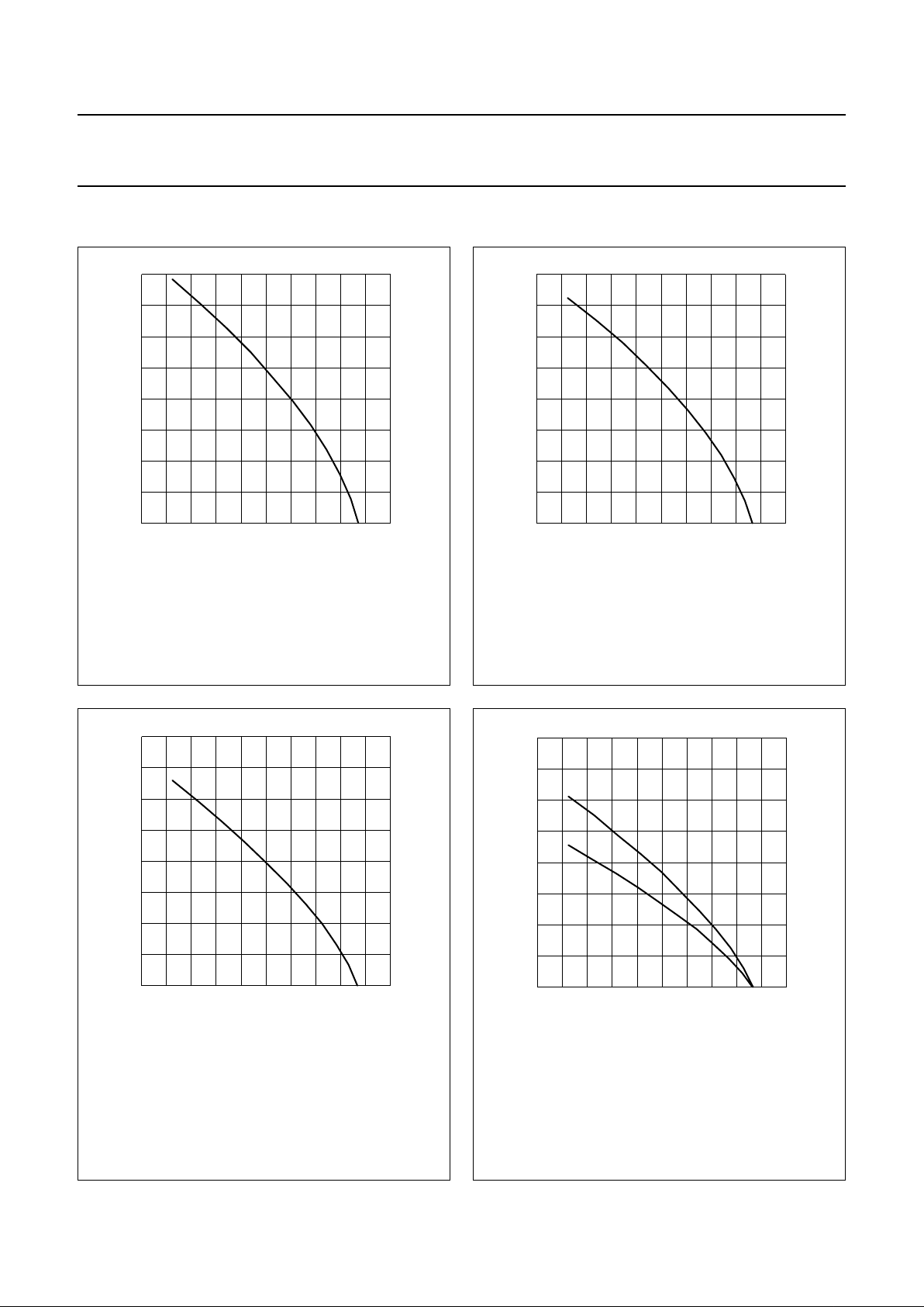
Fig.2 Maximum permissible average forward
current as a function of tie-point temperature
(including losses due to reverse leakage).
BYG80A toD
Switched mode application; VR=V
RRMmax
; δ = 0.5; a = 1.42.
handbook, halfpage
0 200
100
T
tp
(oC)
4
3
I
F(AV)
(A)
1
0
2
MGL081
BYG80F and G
Switched mode application; VR=V
RRMmax
; δ = 0.5; a= 1.42.
Fig.3 Maximum permissible average forward
current as a function of tie-point temperature
(including losses due to reverse leakage).
handbook, halfpage
0 40 200
Ttp (°C)
I
F(AV)
(A)
4
3
1
0
2
80 120 160
MBK454
BYG80J
Switched mode application.
VR=V
RRMmax
; δ = 0.5; a= 1.42.
Fig.4 Maximum permissible average forward
current as a function of tie-point temperature
(including losses due to reverse leakage).
handbook, halfpage
040
I
FAV
(A)
200
4.0
3.0
1.0
0
2.0
80 120 160
Ttp (οC)
MGL094
Fig.5 Maximum permissible average forward
current as a function of ambient temperature
(including losses due to reverse leakage).
BYG80A to D
Switched mode application; VR=V
RRMmax
; δ = 0.5; a= 1.42
Device mounted as shown in Fig.27;
1: Al
2O3
PCB; 2: epoxy PCB.
handbook, halfpage
0
(1)
(2)
200
100
T
amb
(οC)
2
1.5
I
F(AV)
(A)
0.5
0
1
MGL079

1997 Nov 25 6
Philips Semiconductors Product specification
Ultra fast low-loss
controlled avalanche rectifiers
BYG80 series
BYG80F and G
Switched mode application; VR=V
RRMmax
; δ = 0.5; a= 1.42
Device mounted as shown in Fig.27;
1: Al
2O3
PCB; 2: epoxy PCB.
Fig.6 Maximum permissible average forward
current as a function of ambient temperature
(including losses due to reverse leakage).
handbook, halfpage
0
(1)
(2)
200
100
T
amb
(οC)
2
1.5
I
F(AV)
(A)
0.5
0
1
MGL080
BYG80J
Switched mode application; VR=V
RRMmax
; δ = 0.5; a= 1.42
Device mounted as shown in Fig.27;
1: Al
2O3
PCB; 2: epoxy PCB.
Fig.7 Maximum permissible average forward
current as a function of ambient temperature
(including losses due to reverse leakage).
handbook, halfpage
0 200
0
0.4
0.8
1.2
1.6
40
(1)
(2)
I
F(AV)
(A)
80 120
Tamb (
o
C)
160
MGL092
Fig.8 Maximum repetitive peak forward current as a function of pulse time (square pulse) and duty factor.
BYG80A to D
Ttp= 100 °C; R
th j-tp
= 25 K/W.
V
RRMmax
during 1 - δ; curves include derating for T
j max
at V
RRM
= 200 V.
handbook, full pagewidth
30
0
10
I
FRM
(A)
20
MGL086
10
−2
10
−1
110
t
P
(ms)
10
2
10
3
10
4
δ = 0.05
1
0.1
0.2
0.5
 Loading...