

Philips byg60 DATASHEETS
DISCRETE SEMICONDUCTORS
DATA SH EET
, halfpage
M3D168
BYG60 series
Fast soft-recovery
controlled avalanche rectifiers
Product specification
Supersedes data of 1996 June 05
2000 Jul 03
Philips Semiconductors Product specification
Fast soft-recovery
controlled avalanche rectifiers
FEATURES
• Glass passivated
• High maximum operating
temperature
• Low leakage current
• Excellent stability
• Guaranteed avalanche energy
absorption capability
• UL 94V-O classified plastic
package
• Shipped in 12 mm embossed tape.
LIMITING VALUES
In accordance with the Absolute Maximum Rating System (IEC 60134).
DESCRIPTION
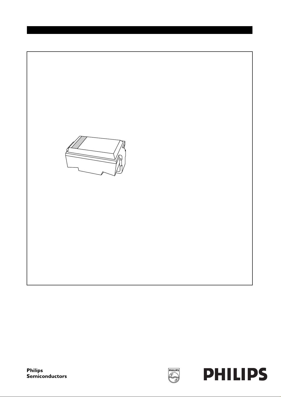
DO-214AC surface mountable
package with glass passivated chip.
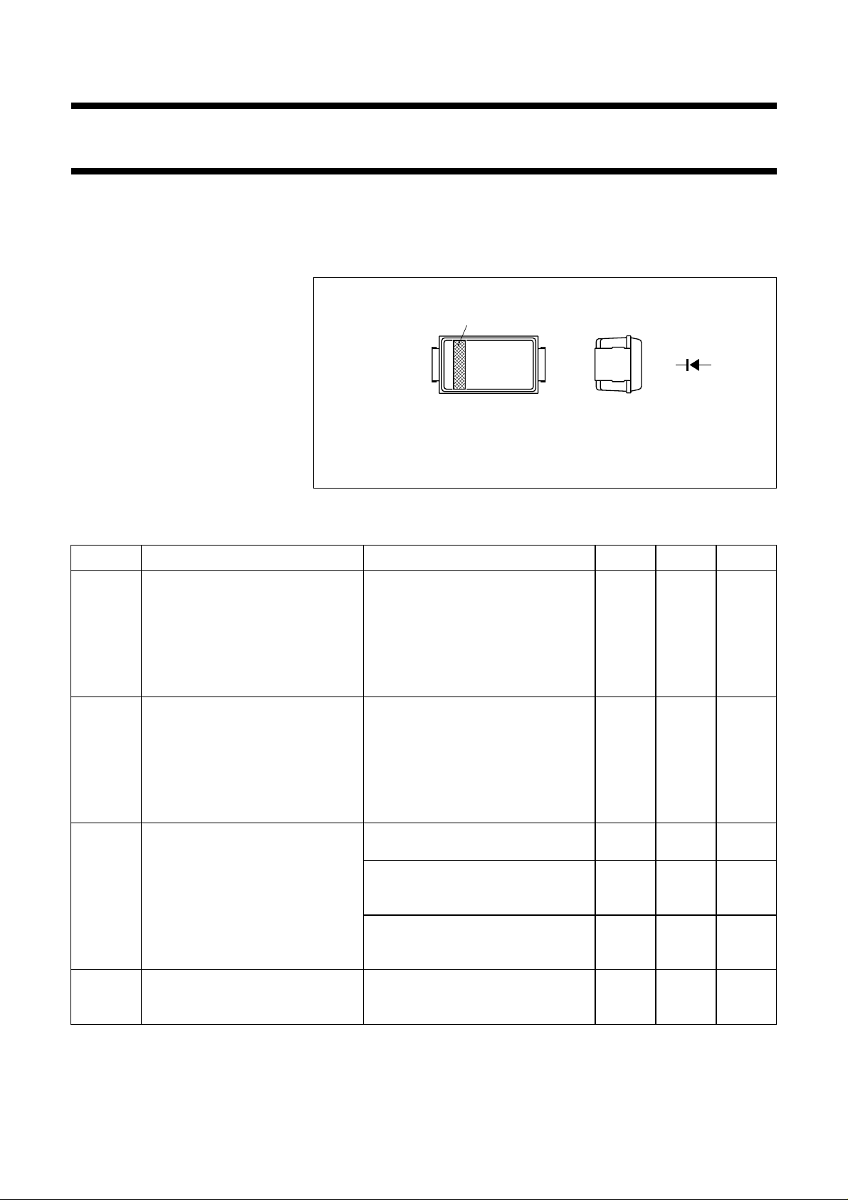
handbook, 4 columns
ka
Top view Side view
cathode
band
Fig.1 Simplified outline (DO-214AC; SOD106) and symbol.
BYG60 series
Thewell-definedvoid-freecaseisofa
transfer-moulded thermo-setting
plastic.
MSA474
SYMBOL PARAMETER CONDITIONS MIN. MAX. UNIT
V
RRM
repetitive peak reverse voltage
BYG60D − 200 V
BYG60G − 400 V
BYG60J − 600 V
BYG60K − 800 V
BYG60M − 1000 V
V
R
continuous reverse voltage
BYG60D − 200 V
BYG60G − 400 V
BYG60J − 600 V
BYG60K − 800 V
BYG60M − 1000 V
I
F(AV)
average forward current averaged over any 20 ms period;
− 1.9 A
Ttp= 100 °C; see Fig.2
averaged over any 20 ms period;
Al
printed-circuit board mounting
2O3
(see Fig.7); T
=60°C; see Fig.3
amb
averaged over any 20 ms period;
− 0.9 A
− 0.65 A
epoxy printed-circuit board mounting
I
FSM
(see Fig.7); T
non-repetitive peak forward current t = 10 ms half sine wave;
Tj=T
j max
VR=V
RRMmax
=60°C; see Fig.3
amb
prior to surge;
− 25 A
2000 Jul 03 2

Philips Semiconductors Product specification
Fast soft-recovery
BYG60 series
controlled avalanche rectifiers
SYMBOL PARAMETER CONDITIONS MIN. MAX. UNIT
E
RSM
non-repetitive peak reverse
avalanche energy
BYG60D to J − 10 mJ
BYG60K and M − 7mJ
T
stg
T
j
storage temperature −65 +175 °C
junction temperature see Fig.4 −65 +175 °C
ELECTRICAL CHARACTERISTICS
Tj=25°C unless otherwise specified.
SYMBOL PARAMETER CONDITIONS MIN. TYP. MAX. UNIT
V
V
F
(BR)R
forward voltage IF= 1 A; Tj=T
= 1 A; see Fig.5 −−1.2 V
I
F
reverse avalanche
IR= 0.1 mA
breakdown voltage
BYG60D 300 −−V
BYG60G 500 −−V
BYG60J 700 −−V
BYG60K 900 −−V
BYG60M 1100 −−V
I
R
reverse current VR=V
see Fig.6
V
R=VRRMmax
see Fig.6
t
rr
C
d
reverse recovery time when switched from IF= 0.5 A to
BYG60D to J −−250 ns
BYG60K and M −−300 ns
IR= 1 A; measured at IR= 0.25 A;
see Fig.8
diode capacitance VR= 0 V; f = 1 MHz
BYG60D to J − 30 − pF
BYG60K and M − 25 − pF
L = 120 mH; Tj=T
j max
inductive load switched off
see Fig.5 −−0.98 V
j max;
;
RRMmax
; Tj= 165 °C;
prior to surge;
−−5µA
−−100 µA
THERMAL CHARACTERISTICS
SYMBOL PARAMETER CONDITIONS VALUE UNIT
R
R
th j-tp
th j-a
thermal resistance from junction to tie-point 25 K/W
thermal resistance from junction to ambient note 1 100 K/W
note 2 150 K/W
Notes
1. Device mounted on Al
printed-circuit board, 0.7 mm thick; thickness of copper ≥35 µm, see Fig.7.
2O3
2. Device mounted on epoxy-glass printed-circuit board, 1.5 mm thick; thickness of copper ≥40 µm, see Fig.7.
For more information please refer to the
‘General Part of associated Handbook’
.
2000 Jul 03 3
 Loading...