

Philips BYD73C, BYD73B, BYD73A, BYD73G, BYD73F Datasheet
...
DISCRETE SEMICONDUCTORS
DATA SH EET
k, halfpage
M3D119
BYD73 series
Ultra fast low-loss
controlled avalanche rectifiers
Product specification
Supersedes data of 1996 May 24
File under Discrete Semiconductors, SC01
1996 Sep 18
Philips Semiconductors Product specification
Ultra fast low-loss
BYD73 series
controlled avalanche rectifiers
FEATURES
• Glass passivated
• High maximum operating
temperature
DESCRIPTION
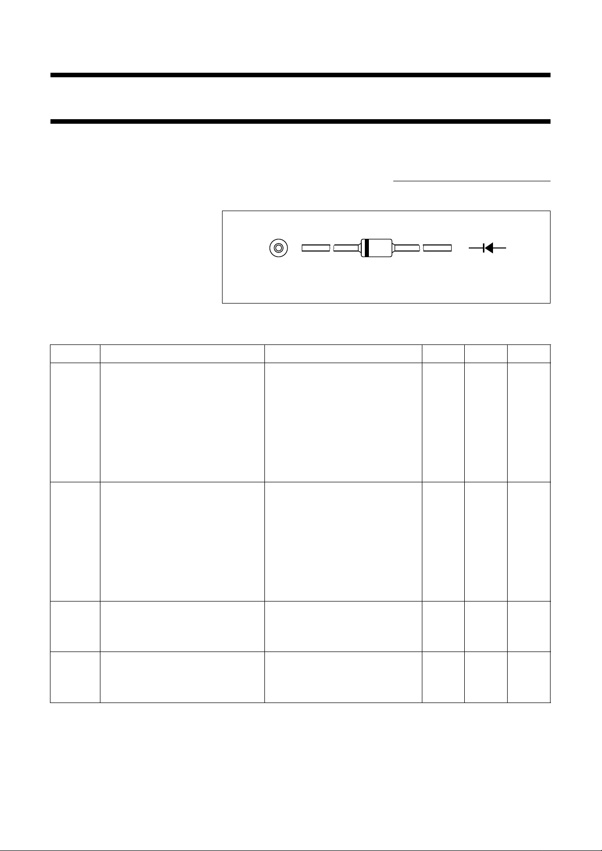
Cavity free cylindrical glass SOD81
package through Implotec
(1)
technology. This package is
• Low leakage current
• Excellent stability
• Guaranteed avalanche energy
absorption capability
handbook, 4 columns
• Available in ammo-pack.
Fig.1 Simplified outline (SOD81) and symbol.
LIMITING VALUES
In accordance with the Absolute Maximum Rating System (IEC 134).
SYMBOL PARAMETER CONDITIONS MIN. MAX. UNIT
V
RRM
repetitive peak reverse voltage
BYD73A − 50 V
BYD73B − 100 V
BYD73C − 150 V
BYD73D − 200 V
BYD73E − 250 V
BYD73F − 300 V
BYD73G − 400 V
V
R
continuous reverse voltage
BYD73A − 50 V
BYD73B − 100 V
BYD73C − 150 V
BYD73D − 200 V
BYD73E − 250 V
BYD73F − 300 V
BYD73G − 400 V
I
F(AV)
I
F(AV)
average forward current Ttp=55°C; lead length = 10 mm;
BYD73A to D − 1.75 A
BYD73E to G − 1.70 A
average forward current T
BYD73A to D − 1.00 A
BYD73E to G − 0.95 A
see Figs 2 and 3;
averaged over any 20 ms period;
see also Figs 10 and 11
=60°C; PCB mounting (see
amb
Fig.16); see Figs 4 and 5;
averaged over any 20 ms period;
see also Figs 10 and 11
hermetically sealed and fatigue free
as coefficients of expansion of all
used parts are matched.
(1) Implotec is a trademark of Philips.
ak
MAM123
1996 Sep 18 2

Philips Semiconductors Product specification
Ultra fast low-loss
BYD73 series
controlled avalanche rectifiers
SYMBOL PARAMETER CONDITIONS MIN. MAX. UNIT
I
FRM
I
FRM
I
FSM
E
RSM
T
stg
T
j
ELECTRICAL CHARACTERISTICS
=25°C unless otherwise specified.
T
j
repetitive peak forward current Ttp=55°C; see Figs 6 and 7
BYD73A to D − 14 A
BYD73E to G − 15 A
repetitive peak forward current T
=60°C; see Figs 8 and 9
amb
BYD73A to D − 8.5 A
BYD73E to G − 9.5 A
non-repetitive peak forward current t = 10 ms half sine wave;
non-repetitive peak reverse
avalanche energy
Tj=T
VR=V
L = 120 mH; Tj=T
surge; inductive load switched off
prior to surge;
j max
RRMmax
j max
prior to
− 25 A
− 10 mJ
storage temperature −65 +175 °C
junction temperature −65 +175 °C
SYMBOL PARAMETER CONDITIONS MIN. TYP. MAX. UNIT
V
F
forward voltage IF= 1 A; Tj=T
BYD73A to D −−0.75 V
see Figs 12 and 13
j max
;
BYD73E to G −−0.83 V
V
F
forward voltage IF=1A;
BYD73A to D −−0.98 V
see Figs 12 and 13
BYD73E to G −−1.05 V
V
(BR)R
reverse avalanche breakdown
IR= 0.1 mA
voltage
BYD73A 55 −−V
BYD73B 110 −−V
BYD73C 165 −−V
BYD73D 220 −−V
BYD73E 275 −−V
BYD73F 330 −−V
BYD73G 440 −−V
I
R
reverse current VR=V
RRMmax
;
−− 1µA
see Fig.14
V
R=VRRMmax
;
−−100 µA
Tj= 165 °C; see Fig.14
t
rr
reverse recovery time when switched from
BYD73A to D −−25 ns
BYD73E to G −−50 ns
IF= 0.5 A to IR=1A;
measured at IR= 0.25 A;
see Fig.18
1996 Sep 18 3
Philips Semiconductors Product specification
Ultra fast low-loss
BYD73 series
controlled avalanche rectifiers
SYMBOL PARAMETER CONDITIONS MIN. TYP. MAX. UNIT
C
d
dI
R
-------dt
THERMAL CHARACTERISTICS
SYMBOL PARAMETER CONDITIONS VALUE UNIT
R
th j-tp
R
th j-a
Note
1. Device mounted on an epoxy-glass printed-circuit board, 1.5 mm thick; thickness of Cu-layer ≥40 µm, see Fig.16.
For more information please refer to the
diode capacitance f = 1 MHz; VR=0V;
BYD73A to D − 50 − pF
BYD73E to G − 40 − pF
maximum slope of reverse recovery
current
BYD73A to D −− 4A/µs
BYD73E to G −− 5A/µs
thermal resistance from junction to tie-point lead length = 10 mm 60 K/W
thermal resistance from junction to ambient note 1 120 K/W
see Fig.15
when switched from
I
= 1 A to VR≥ 30 V
F
and dIF/dt = −1A/µs;
see Fig.17
‘General Part of Handbook SC01.’
1996 Sep 18 4
 Loading...