

Philips BYD72E, BYD72C, BYD72A, BYD72G, BYD72F Datasheet

DISCRETE SEMICONDUCTORS
DATA SH EET
ook, halfpage
M3D423
BYD72 series
Ultra fast low-loss
controlled avalanche rectifiers
Preliminary specification
1998 Dec 03
Philips Semiconductors Preliminary specification
Ultra fast low-loss
BYD72 series
controlled avalanche rectifiers
FEATURES
• Glass passivated
• High maximum operating
temperature
DESCRIPTION
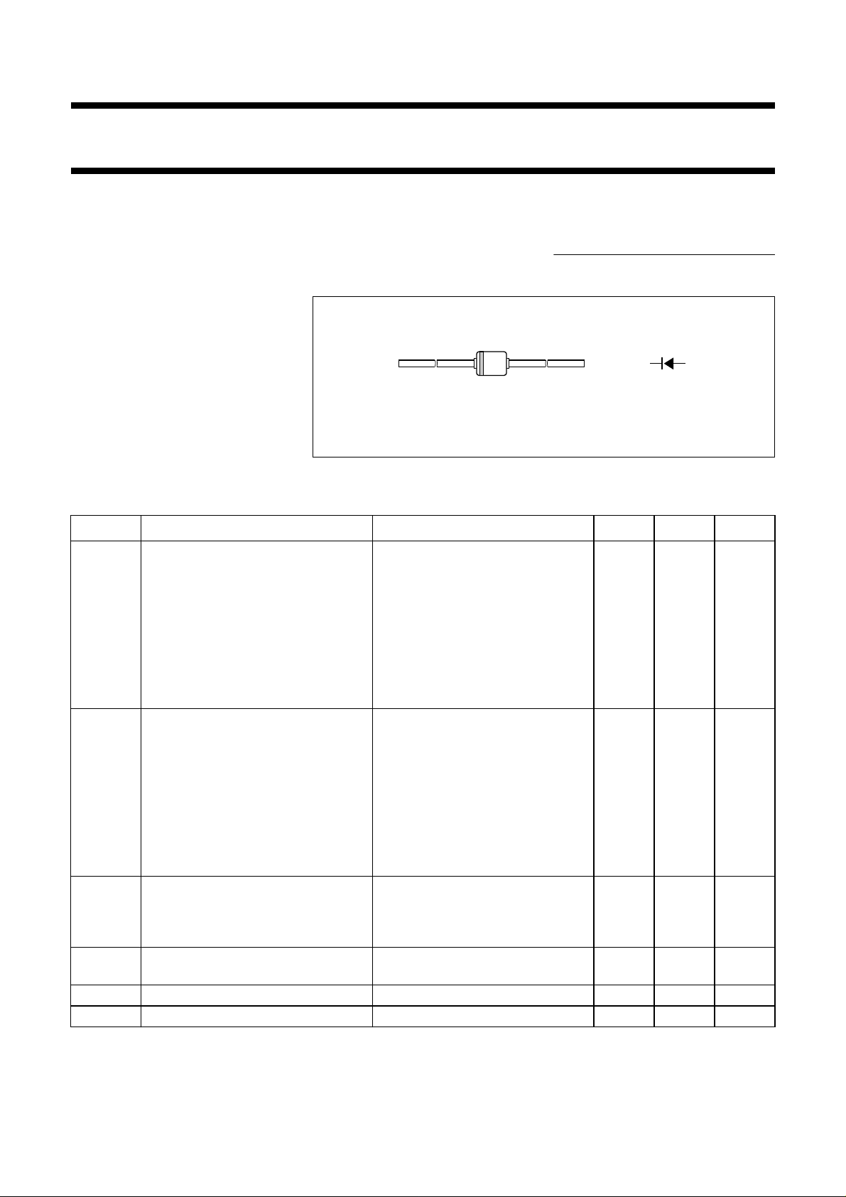
Cavity free cylindrical glass SOD120
package through Implotec
(1)
technology. This package is
• Low leakage current
• Excellent stability
• Guaranteed avalanche energy
absorption capability
handbook, halfpage
ka
• Available in ammo-pack.
Fig.1 Simplified outline (SOD120) and symbol.
LIMITING VALUES
In accordance with the Absolute Maximum Rating System (IEC 134).
SYMBOL PARAMETER CONDITIONS MIN. MAX. UNIT
V
RRM
repetitive peak reverse voltage
BYD72A − 50 V
BYD72B − 100 V
BYD72C − 150 V
BYD72D − 200 V
BYD72E − 250 V
BYD72F − 300 V
BYD72G − 400 V
V
R
continuous reverse voltage
BYD72A − 50 V
BYD72B − 100 V
BYD72C − 150 V
BYD72D − 200 V
BYD72E − 250 V
BYD72F − 300 V
BYD72G − 400 V
I
F(AV)
I
FSM
T
stg
T
j
average forward current T
BYD72A to D − 1.02 A
BYD72E to G − 0.95 A
=25°C; printed-circuit board
amb
mounting, pitch 5 mm, see Fig.8;
averaged over any 20 ms period;
see Figs 2 and 3
non-repetitive peak forward current t = 10 ms half sine wave;
Tj=25°C; VR=V
RRMmax
storage temperature −65 +175 °C
junction temperature see Fig.7 −65 +175 °C
hermetically sealed and fatigue free
as coefficients of expansion of all
used parts are matched.
(1) Implotec is a trademark of Philips.
MGL571
− 15 A
1998 Dec 03 2
Philips Semiconductors Preliminary specification
Ultra fast low-loss
BYD72 series
controlled avalanche rectifiers
ELECTRICAL CHARACTERISTICS
T
=25°C unless otherwise specified.
j
SYMBOL PARAMETER CONDITIONS MAX. UNIT
V
F
I
R
t
rr
V
FRM
THERMAL CHARACTERISTICS
forward voltage IF= 1 A; see Figs 4 and 5
BYD72A to D 0.98 V
BYD72E to G 1.05 V
reverse current VR=V
V
R=VRRMmax
RRMmax
; Tj= 165 °C; see Fig.6 100 µA
1 µA
reverse recovery time when switched from IF= 0.5 A to IR=1A;
BYD72A to D 25 ns
measured at IR= 0.25 A; see Fig.9
BYD72E to G 50 ns
forward recovery voltage when switched to IF= 1 A in 50 ns
BYD72A to D 1.55 V
BYD72E to G 3.40 V
SYMBOL PARAMETER CONDITIONS VALUE UNIT
R
th j-a
thermal resistance from junction to ambient note 1 150 K/W
Note
1. Device mounted on an epoxy-glass printed-circuit board, 1.5 mm thick; thickness of copper layer ≥40 µm,
pitch 5 mm; see Fig.8.
1998 Dec 03 3
 Loading...