

Philips BYD47-18, BYD47-16 Datasheet
DISCRETE SEMICONDUCTORS
DATA SH EET
book, halfpage
M3D121
BYD47 series
Fast soft-recovery rectifiers
Product specification
Supersedes data of November 1994
File under Discrete Semiconductors, SC01
1996 Jun 05
Philips Semiconductors Product specification
Fast soft-recovery rectifiers BYD47 series
FEATURES
• Glass passivated
• High maximum operating
temperature
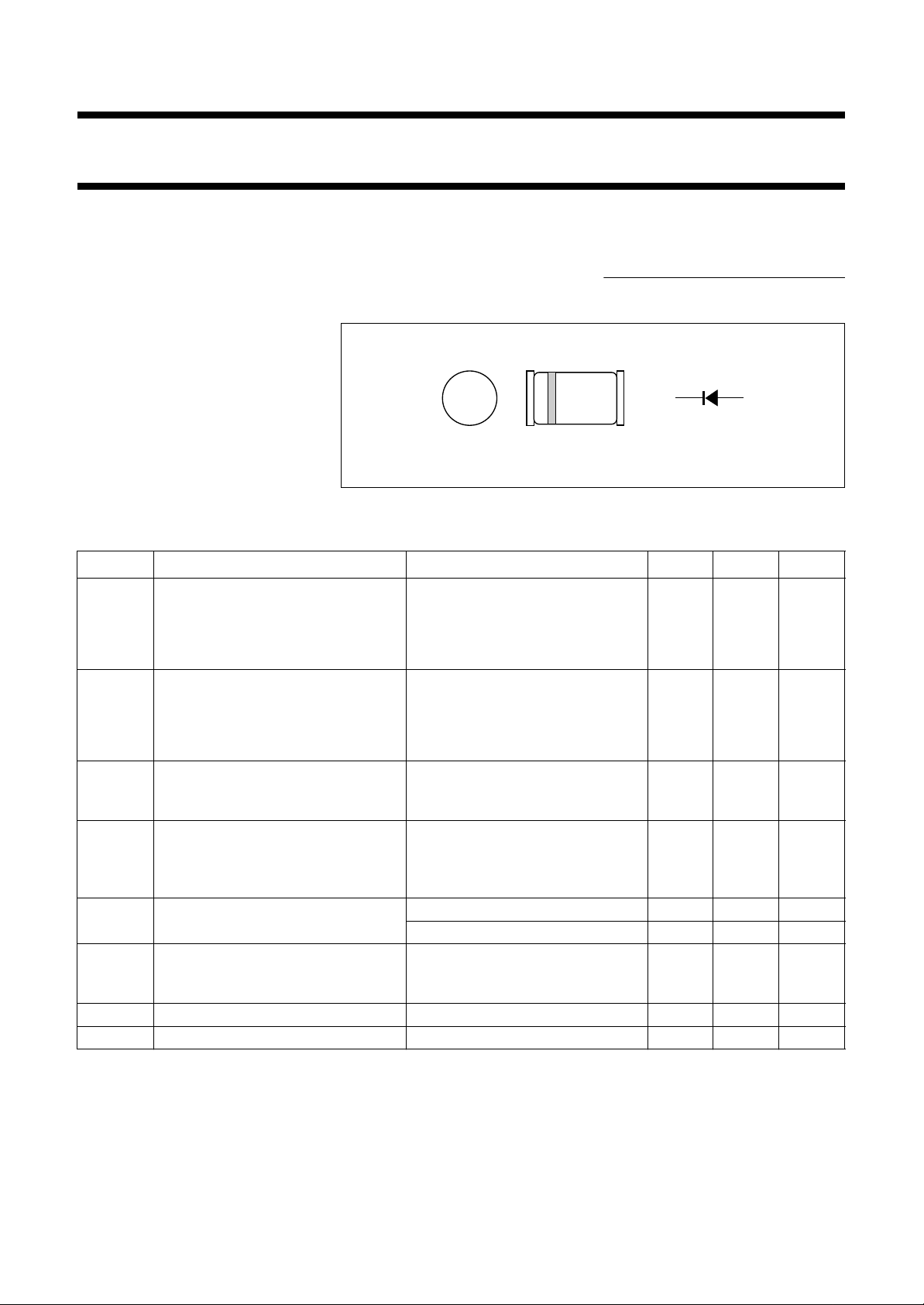
DESCRIPTION
Cavity free cylindrical glass SOD87
package through Implotec
(1)
technology. This package is
hermetically sealed and fatigue free
as coefficients of expansion of all
used parts are matched.
(1) Implotec is a trademark of Philips.
• Low leakage current
• Excellent stability
• Shipped in 8 mm embossed tape
handbook, 4 columns
ka
• Smallest surface mount
rectifier outline.
MAM061
Fig.1 Simplified outline (SOD87) and symbol.
LIMITING VALUES
In accordance with the Absolute Maximum Rating System (IEC 134).
SYMBOL PARAMETER CONDITIONS MIN. MAX. UNIT
V
RSM
non-repetitive peak reverse voltage
BYD47-16 − 1700 V
BYD47-18 − 1900 V
BYD47-20 − 2100 V
V
RRM
repetitive peak reverse voltage
BYD47-16 − 1600 V
BYD47-18 − 1800 V
BYD47-20 − 2000 V
I
F(AV)
average forward current Ttp= 105 °C; see Fig. 2;
− 0.80 A
averaged over any 20 ms period;
see also Fig. 6
I
F(AV)
average forward current T
=25°C; PCB mounting (see
amb
− 0.34 A
Fig.11); see Fig. 3;
averaged over any 20 ms period;
see also Fig. 6
I
FRM
I
FSM
T
T
stg
j
repetitive peak forward current Ttp=85°C; see Fig. 4 − 8.0 A
=65°C; see Fig. 5 − 2.8 A
T
amb
non-repetitive peak forward current t = 10 ms half sine wave;
Tj=T
VR=V
prior to surge;
j max
RRMmax
− 10 A
storage temperature −65 +175 °C
junction temperature see Fig. 7 −65 +175 °C
1996 Jun 05 2
Philips Semiconductors Product specification
Fast soft-recovery rectifiers BYD47 series
ELECTRICAL CHARACTERISTICS
T
=25°C unless otherwise specified.
j
SYMBOL PARAMETER CONDITIONS TYP. MAX. UNIT
V
I
t
C
F
R
rr
dI
-------dt
d
R
forward voltage IF= 1 A; Tj=T
= 1 A; see Fig. 8 − 2.40 V
I
F
reverse current VR=V
RRMmax
; see Fig. 8 − 2.05 V
j max
;
− 5 µA
see Fig. 9
V
R=VRRMmax
; Tj= 125 °C;
− 50 µA
see Fig. 9
reverse recovery time when switched from IF= 0.5 A to
− 300 ns
IR= 1 A; measured at IR= 0.25 A;
see Fig. 12
diode capacitance f = 1 MHz; VR= 0 V; see Fig. 10 15 − pF
maximum slope of reverse recovery
current
when switched from I
VR≥ 30 V and dIF/dt = −1A/µs;
= 1 A to
F
− 5A/µs
see Fig.13
THERMAL CHARACTERISTICS
SYMBOL PARAMETER CONDITIONS VALUE UNIT
R
R
th j-tp
th j-a
thermal resistance from junction to tie-point 30 K/W
thermal resistance from junction to ambient note 1 150 K/W
Note
1. Device mounted on an epoxy-glass printed-circuit board, 1.5 mm thick; thickness of Cu-layer ≥40 µm, see Fig.11.
For more information please refer to the
‘General Part of Handbook SC01.’
1996 Jun 05 3
 Loading...