

Philips byd13 DATASHEETS
DISCRETE SEMICONDUCTORS
DATA SH EET
ook, halfpage
M3D119
BYD13 series
Controlled avalanche rectifiers
Product specification
Supersedes data of April 1992
1996 May 24
Philips Semiconductors Product specification
Controlled avalanche rectifiers BYD13 series
FEATURES
• Glass passivated
• High maximum operating
temperature
• Low leakage current
• Excellent stability
• Guaranteed avalanche energy
absorption capability
• Available in ammo-pack.
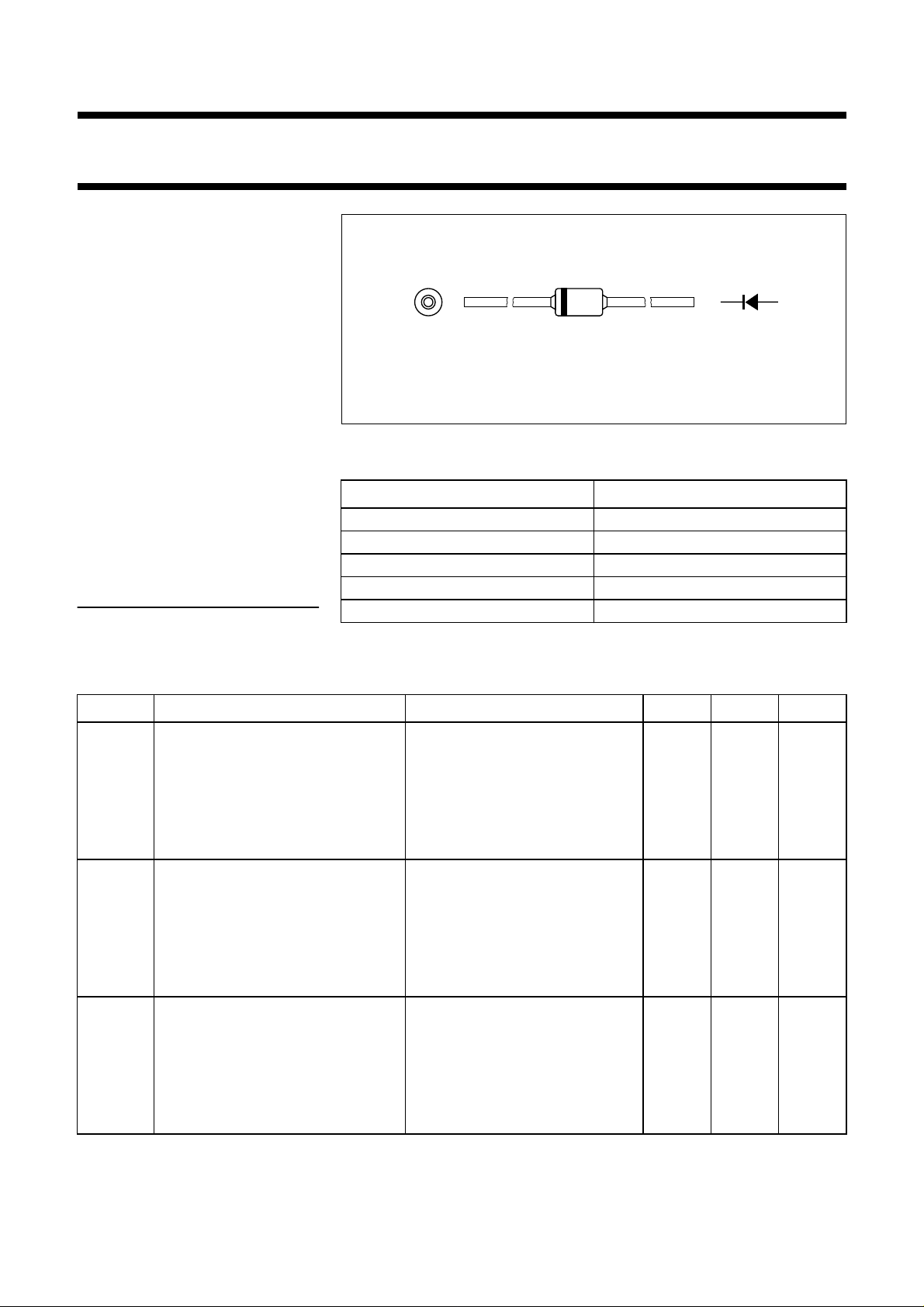
handbook, 4 columns
Fig.1 Simplified outline (SOD81) and symbol.
ak
MAM123
DESCRIPTION
MARKING
Cavity free cylindrical glass package
through Implotec
(1)
technology.
This package is hermetically sealed
and fatigue free as coefficients of
expansion of all used parts are
matched.
(1) Implotec is a trademark of Philips.
BYD13D 13D PH
BYD13G 13G PH
BYD13J 13J PH
BYD13K 13K PH
BYD13M 13M PH
TYPE NUMBER MARKING CODE
LIMITING VALUES
In accordance with the Absolute Maximum Rating System (IEC 134).
SYMBOL PARAMETER CONDITIONS MIN. MAX. UNIT
V
RRM
repetitive peak reverse voltage
BYD13D − 200 V
BYD13G − 400 V
BYD13J − 600 V
BYD13K − 800 V
BYD13M − 1000 V
V
RWM
crest working reverse voltage
BYD13D − 200 V
BYD13G − 400 V
BYD13J − 600 V
BYD13K − 800 V
BYD13M − 1000 V
V
R
continuous reverse voltage
BYD13D − 200 V
BYD13G − 400 V
BYD13J − 600 V
BYD13K − 800 V
BYD13M − 1000 V
1996 May 24 2

Philips Semiconductors Product specification
Controlled avalanche rectifiers BYD13 series
SYMBOL PARAMETER CONDITIONS MIN. MAX. UNIT
I
F(AV)
I
FSM
E
RSM
T
stg
T
j
average forward current Ttp=55°C; lead length = 10 mm;
averaged over any 20 ms period;
see Figs 2 and 4
=65°C; PCB mounting
T
amb
(see Fig.9);
averaged over any 20 ms period;
see Figs 3 and 4
non-repetitive peak forward current t = 10 ms half sinewave;
non-repetitive peak reverse
avalanche energy
Tj=T
VR=V
L = 120 mH; Tj=T
surge; inductive load switched off
prior to surge;
j max
RRMmax
j max
prior to
storage temperature −65 +175 °C
junction temperature
see Fig.5
− 1.40 A
− 0.75 A
− 20 A
− 7
mJ
−65 +175 °C
ELECTRICAL CHARACTERISTICS
=25°C; unless otherwise specified.
T
j
SYMBOL PARAMETER CONDITIONS MIN. TYP. MAX. UNIT
V
V
F
(BR)R
forward voltage IF=1A; Tj=T
I
= 1 A; see Fig.6 −−1.05 V
F
reverse avalanche
IR= 0.1 mA
see Fig.6 −−0.93 V
j max;
breakdown voltage
BYD13D 225 −−V
BYD13G 450 −−V
BYD13J 650 −−V
BYD13K 900 −−V
BYD13M 1100 −−V
I
R
t
rr
reverse current VR=V
V
R=VRRMmax
; see Fig.7 −−1µA
RRMmax
; Tj= 165 °C; see Fig.7 −−100 µA
reverse recovery time when switched from IF= 0.5 A to IR=1A;
− 3 −
µs
measured at IR= 0.25 A; see Fig.10
C
d
diode capacitance VR= 0 V; f = 1 MHz; see Fig.8 − 21 −
pF
THERMAL CHARACTERISTICS
SYMBOL PARAMETER CONDITIONS VALUE UNIT
R
R
th j-tp
th j-a
thermal resistance from junction to tie-point lead length = 10 mm 60 K/W
thermal resistance from junction to ambient note 1 120 K/W
Note
1. Device mounted on epoxy-glass printed-circuit board, 1.5 mm thick; thickness of copper ≥40 µm, see Fig.9.
For more information please refer to the
“General Part of associated Handbook”
.
1996 May 24 3
 Loading...