

Philips BYC8B-600 Datasheet
Philips Semiconductors Product specification
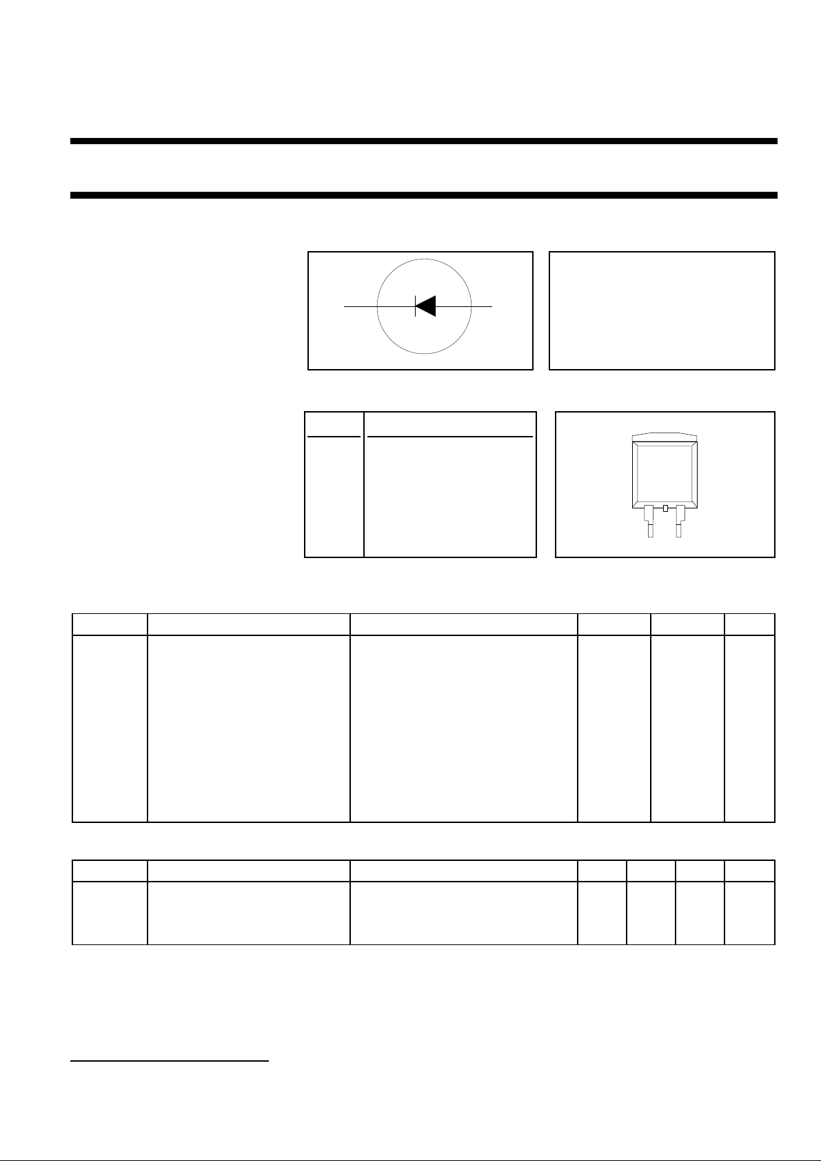
Rectifier diode BYC8B-600
ultrafast, low switching loss
FEATURES SYMBOL QUICK REFERENCE DATA
• Extremely fast switching VR = 600 V
• Low reverse recovery current
• Low thermal resistance VF ≤ 1.85 V
• Reduces switching losses in
associated MOSFET I
APPLICATIONS PINNING SOT404
k a
tab 3
= 8 A
F(AV)
trr = 19 ns (typ)
• Active power factor correction PIN DESCRIPTION
tab
• Half-bridge lighting ballasts
• Half-bridge/ full-bridge switched 1 no connection
mode power supplies.
2 cathode
1
The BYC8B-600 is supplied in the
SOT404 surface mounting 3 anode
package.
2
tab cathode
13
LIMITING VALUES
Limiting values in accordance with the Absolute Maximum System (IEC 134).
SYMBOL PARAMETER CONDITIONS MIN. MAX. UNIT
V
V
V
I
F(AV)
I
FRM
I
FSM
T
T
RRM
RWM
R
stg
j
Peak repetitive reverse voltage - 600 V
Crest working reverse voltage - 600 V
Continuous reverse voltage Tmb ≤ 110 ˚C - 500 V
Average forward current δ = 0.5; with reapplied V
Tmb ≤ 82 ˚C
Repetitive peak forward current δ = 0.5; with reapplied V
Tmb ≤ 82 ˚C
1
1
;-8A
RRM(max)
; - 16 A
RRM(max)
Non-repetitive peak forward t = 10 ms - 55 A
current. t = 8.3 ms - 60 A
sinusoidal; Tj = 150˚C prior to surge
Storage temperature -40 150 ˚C
with reapplied V
RWM(max)
Operating junction temperature - 150 ˚C
THERMAL RESISTANCES
SYMBOL PARAMETER CONDITIONS MIN. TYP. MAX. UNIT
R
th j-mb
R
th j-a
1 it is not possible to make connection to pin 2 of the SOT404 package
October 1998 1 Rev 1.200
Thermal resistance junction to - - 2.2 K/W
mounting base
Thermal resistance junction to minimum footprint, FR4 board - 50 - K/W
ambient
Philips Semiconductors Product specification
Rectifier diode BYC8B-600
ultrafast, low switching loss
ELECTRICAL CHARACTERISTICS
Tj = 25 ˚C unless otherwise stated
SYMBOL PARAMETER CONDITIONS MIN. TYP. MAX. UNIT
V
F
I
R
t
rr
t
rr
I
rrm
V
fr
Forward voltage IF = 8 A; Tj = 150˚C - 1.4 1.85 V
IF = 16 A; Tj = 150˚C - 1.7 2.3 V
IF = 8 A; - 2.0 2.8 V
Reverse current VR = 600 V - 9 150 µA
VR = 500 V; Tj = 100 ˚C - 1.1 3.0 mA
Reverse recovery time IF = 8 A to VR = 400 V; - 19 - ns
dIF/dt = 500 A/µs
Reverse recovery time IF = 8 A to VR = 400 V; - 32 40 ns
dIF/dt = 500 A/µs; Tj = 125˚C
Peak reverse recovery current IF = 8 A to VR = 400 V; - 9.5 12 A
dIF/dt = 500 A/µs; Tj = 125˚C
Forward recovery voltage IF = 10 A; dIF/dt = 100 A/µs-810V
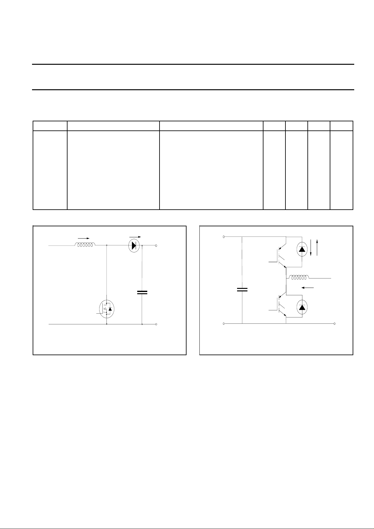
IL
Vin
150 uH
typ
500 V MOSFET
ID
Vo = 400 V d.c.
OUTPUT DIODE
Fig.1. Typical application, output rectifier in boost
converter power factor correction circuit. Continuous
conduction, mode where the transistor turns on whilst
forward current is still flowing in the diode.
Vin = 400 V d.c.
Vin
IFIR
inductive load
IL
Fig.2. Typical application, freewheeling diode in half
bridge converter. Continuous conduction mode, where
each transistor turns on whilst forward current is still
flowing in the other bridge leg diode.
October 1998 2 Rev 1.200
 Loading...