

Philips buk7230 55a DATASHEETS

1. Description
2. Features
BUK7230-55A
TrenchMOS™ standard level FET
Rev. 01 — 29 September 2000 Product specification
N-channel enhancement mode field-effect powertransistorina plastic package using
TrenchMOS™1 technology, featuring very low on-state resistance.
Product availability:
BUK7230-55A in SOT428 (D-PAK).
■ TrenchMOS™ technology
■ Q101 compliant
■ 175 °C rated
■ Standard level compatible.
3. Applications
c
c
■ Automotive and general purpose power switching:
◆ 12 V and 24 V loads
◆ Motors, lamps and solenoids.
4. Pinning information
Table 1: Pinning: SOT428 (D-PAK), simplified outline and symbol
Pin Description Simplified outline Symbol
1 gate (g)
2 drain (d)
3 source (s)
mb mounting base;
connected to
drain (d)
1. TrenchMOS is a trademark of Royal Philips Electronics.
mb
2
13
Top view
SOT428 (D-PAK)
MBK091
g
MBB076
d
s

Philips Semiconductors
BUK7230-55A
TrenchMOS™ standard level FET
5. Quick reference data
Table 2: Quick reference data
Symbol Parameter Conditions Typ Max Unit
V
I
P
T
R
DS
D
tot
j
DSon
drain-source voltage (DC) − 55 V
drain current (DC) Tmb=25°C; VGS=10V − 38 A
total power dissipation Tmb=25°C − 88 W
junction temperature − 175 °C
drain-source on-state resistance VGS= 10 V; ID= 25 A 26 30 mΩ
= 175°C − 60 mΩ
T
j
6. Limiting values
Table 3: Limiting values
In accordance with the Absolute Maximum Rating System (IEC 60134).
Symbol Parameter Conditions Min Max Unit
V
DS
V
DGR
V
GS
I
D
I
DM
P
tot
T
stg
T
j
Source-drain diode
I
DR
I
DRM
Avalanche ruggedness
W
DSS
drain-source voltage (DC) − 55 V
drain-gate voltage (DC) RGS=20kΩ−55 V
gate-source voltage (DC) −±20 V
drain current (DC) Tmb=25°C; VGS=5V;
− 38 A
Figure 2 and 3
T
= 100 °C; VGS=5V;Figure 2 − 27 A
mb
peak drain current Tmb=25°C; pulsed; tp≤ 10 µs;
[1]
− 150 A
Figure 3
total power dissipation Tmb=25°C; Figure 1 − 88 W
storage temperature −55 +175 °C
operating junction temperature −55 +175 °C
reverse drain current (DC) Tmb=25°C − 38 A
pulsed reverse drain current Tmb=25°C; pulsed; tp≤ 10 µs − 150 A
non-repetitive avalanche energy unclamped inductive load; ID=34A;
≤ 55 V; VGS= 10 V; RGS=50Ω;
V
DS
starting T
=25°C
j
− 58 mJ
[1] IDM is limited by chip, not package.
9397 750 07568
Product specification Rev. 01 — 29 September 2000 2 of 13
© Philips Electronics N.V. 2000. All rights reserved.
Philips Semiconductors
BUK7230-55A
TrenchMOS™ standard level FET
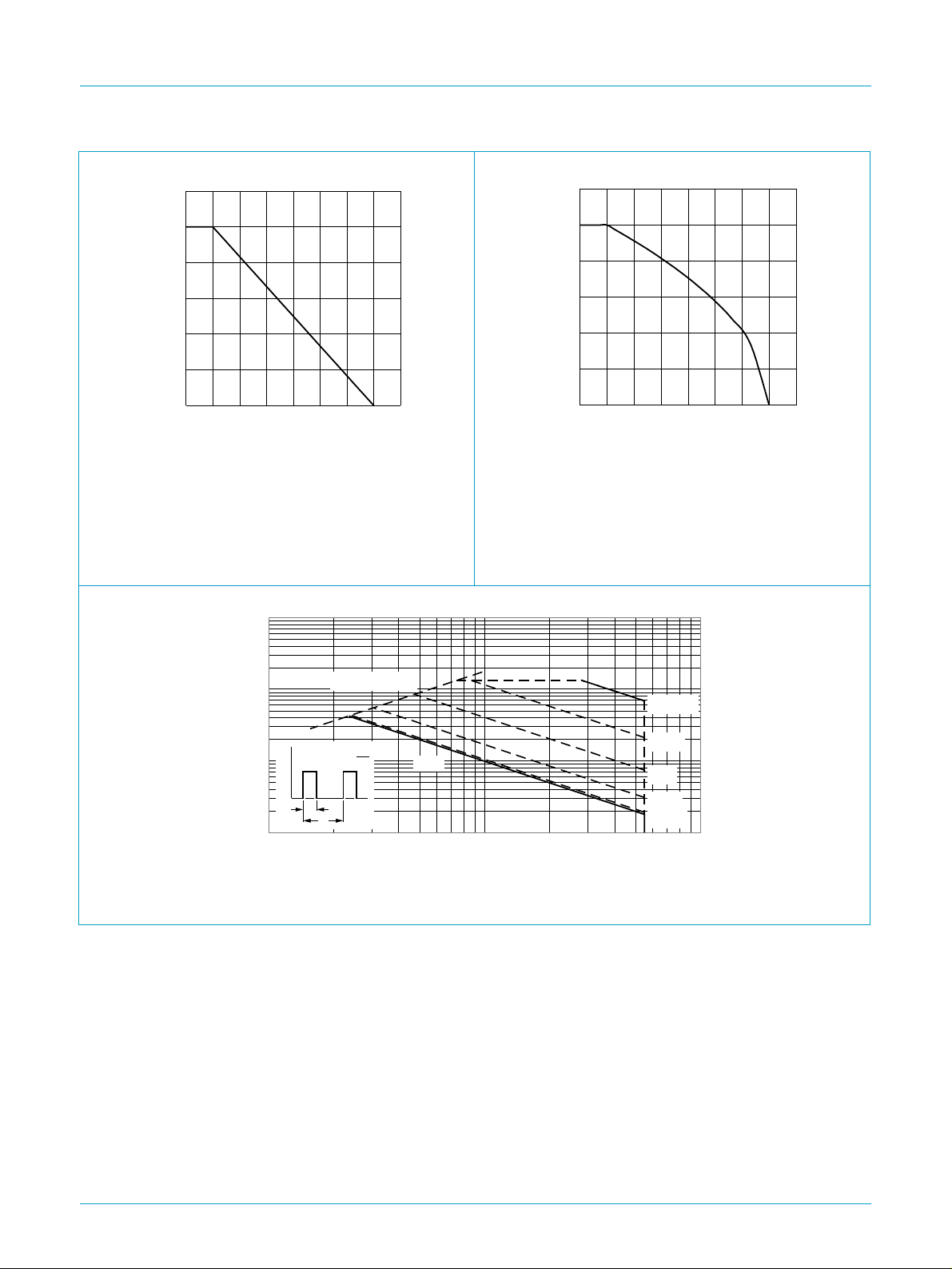
120
P
der
(%)
100
80
60
40
20
0
0 25 50 75 100 125 150 175 200
P
P
der
tot
----------------------
P
tot 25 C°()
100%×=
03aa16
Tmb (oC)
Fig 1. Normalized total power dissipation as a
function of mounting base temperature.
1000
I
D
(A)
120
I
der
(%)
100
80
60
40
20
0
0 25 50 75 100 125 150 175 200
03aa24
Tmb (oC)
VGS≥ 4.5 V
I
I
der
D
------------------ -
I
D25C°()
100%×=
Fig 2. Normalized continuous drain current as a
function of mounting base temperature.
03na49
R
= VDS/ I
T
=25°C; IDM is single pulse.
amb
100
P
10
1
1 10 100
DSon
δ =
t
p
T
D
tp = 10 us
t
p
T
t
D.C.
100 us
1 ms
10 ms
100 ms
VDS (V)
Fig 3. Safe operating area; continuous and peak drain currents as a function of drain-source voltage.
9397 750 07568
© Philips Electronics N.V. 2000. All rights reserved.
Product specification Rev. 01 — 29 September 2000 3 of 13
Philips Semiconductors
BUK7230-55A
TrenchMOS™ standard level FET
7. Thermal characteristics
Table 4: Thermal characteristics
Symbol Parameter Conditions Value Unit
R
th(j-a)
R
th(j-mb)
thermal resistance from junction to ambient Figure 4 71.4 K/W
thermal resistance from junction to mounting
1.7 K/W
base
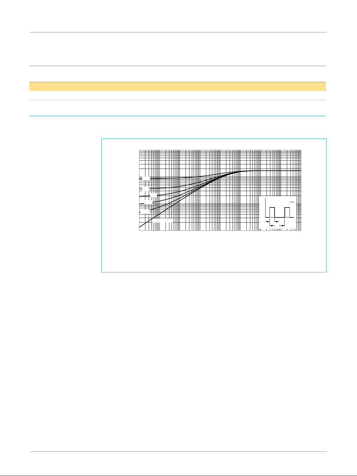
7.1 Transient thermal impedance
10
Z
th(j-mb)
(K/W)
1
10
10
0.5
0.2
0.1
0.05
-1
0.02
Single Shot
-2
-6
10
-5
10
-4
10
-3
10
-2
10
-1
10
P
t
p
1 10 10
03na50
t
p
δ
=
T
t
T
2
tp (s)
Fig 4. Transient thermal impedance from junction to mounting base as a function of
pulse duration.
9397 750 07568
© Philips Electronics N.V. 2000. All rights reserved.
Product specification Rev. 01 — 29 September 2000 4 of 13
 Loading...