

Philips BUK552-100B Datasheet

Philips Semiconductors Product Specification
PowerMOS transistor BUK552-100A/B
Logic level FET
GENERAL DESCRIPTION QUICK REFERENCE DATA
N-channel enhancement mode SYMBOL PARAMETER MAX. MAX. UNIT
logic level field-effect power
transistor in a plastic envelope. BUK552 -100A -100B
The device is intended for use in V
Switched Mode Power Supplies I
(SMPS), motor control, welding, P
DC/DC and AC/DC converters, and T
in automotive and general purpose R
switching applications. resistance; VGS = 5 V
DS
D
tot
j
DS(ON)
PINNING - TO220AB PIN CONFIGURATION SYMBOL
Drain-source voltage 100 100 V
Drain current (DC) 10 8.5 A
Total power dissipation 60 60 W
Junction temperature 175 175 ˚C
Drain-source on-state 0.28 0.35 Ω
PIN DESCRIPTION
tab
d
1 gate
2 drain
3 source
tab drain
123
g
s
LIMITING VALUES
Limiting values in accordance with the Absolute Maximum System (IEC 134)
SYMBOL PARAMETER CONDITIONS MIN. MAX. UNIT
V
V
±V
±V
I
D
I
D
I
DM
P
T
T
DS
DGR
GS
GSM
tot
stg
j
Drain-source voltage - - 100 V
Drain-gate voltage RGS = 20 kΩ - 100 V
Gate-source voltage - - 15 V
Non-repetitive gate-source voltage tp ≤ 50 µs - 20 V
-100A -100B
Drain current (DC) Tmb = 25 ˚C - 10 8.5 A
Drain current (DC) Tmb = 100 ˚C - 7 6 A
Drain current (pulse peak value) Tmb = 25 ˚C - 40 34 A
Total power dissipation Tmb = 25 ˚C - 60 W
Storage temperature - - 55 175 ˚C
Junction Temperature - - 175 ˚C
THERMAL RESISTANCES
SYMBOL PARAMETER CONDITIONS MIN. TYP. MAX. UNIT
R
th j-mb
R
th j-a
April 1993 1 Rev 1.100
Thermal resistance junction to - - 2.5 K/W
mounting base
Thermal resistance junction to - 60 - K/W
ambient

Philips Semiconductors Product Specification
PowerMOS transistor BUK552-100A/B
Logic level FET
STATIC CHARACTERISTICS
Tmb = 25 ˚C unless otherwise specified
SYMBOL PARAMETER CONDITIONS MIN. TYP. MAX. UNIT
V
(BR)DSS
V
GS(TO)
I
DSS
I
DSS
I
GSS
R
DS(ON)
DYNAMIC CHARACTERISTICS
Tmb = 25 ˚C unless otherwise specified
SYMBOL PARAMETER CONDITIONS MIN. TYP. MAX. UNIT
g
fs
C
iss
C
oss
C
rss
t
d on
t
r
t
d off
t
f
L
d
L
d
L
s
Drain-source breakdown VGS = 0 V; ID = 0.25 mA 100 - - V
voltage
Gate threshold voltage VDS = VGS; ID = 1 mA 1.0 1.5 2.0 V
Zero gate voltage drain current VDS = 100 V; VGS = 0 V; Tj = 25 ˚C - 1 10 µA
Zero gate voltage drain current VDS = 100 V; VGS = 0 V; Tj =125 ˚C - 0.1 1.0 mA
Gate source leakage current VGS = ±15 V; VDS = 0 V - 10 100 nA
Drain-source on-state VGS = 5 V; BUK552-100A - 0.25 0.28 Ω
resistance ID = 5.5 A BUK552-100B - 0.3 0.35 Ω
Forward transconductance VDS = 25 V; ID = 5.5 A 4.5 6 - S
Input capacitance VGS = 0 V; VDS = 25 V; f = 1 MHz - 400 600 pF
Output capacitance - 90 120 pF
Feedback capacitance - 35 50 pF
Turn-on delay time VDD = 30 V; ID = 3 A; - 12 18 ns
Turn-on rise time VGS = 5 V; RGS = 50 Ω; - 45 70 ns
Turn-off delay time R
Turn-off fall time - 30 45 ns
= 50 Ω - 5070ns
gen
Internal drain inductance Measured from contact screw on - 3.5 - nH
tab to centre of die
Internal drain inductance Measured from drain lead 6 mm - 4.5 - nH
from package to centre of die
Internal source inductance Measured from source lead 6 mm - 7.5 - nH
from package to source bond pad
REVERSE DIODE LIMITING VALUES AND CHARACTERISTICS
Tmb = 25 ˚C unless otherwise specified
SYMBOL PARAMETER CONDITIONS MIN. TYP. MAX. UNIT
I
DR
I
DRM
V
t
rr
Q
SD
rr
Continuous reverse drain - - - 10 A
current
Pulsed reverse drain current - - - 40 A
Diode forward voltage IF = 10 A ; VGS = 0 V - 1.2 1.5 V
Reverse recovery time IF = 10 A; -dIF/dt = 100 A/µs; - 90 - ns
Reverse recovery charge VGS = 0 V; VR = 30 V - 0.35 - µC
AVALANCHE LIMITING VALUE
Tmb = 25 ˚C unless otherwise specified
SYMBOL PARAMETER CONDITIONS MIN. TYP. MAX. UNIT
W
DSS
April 1993 2 Rev 1.100
Drain-source non-repetitive ID = 10 A ; VDD ≤ 50 V ; - - 30 mJ
unclamped inductive turn-off VGS = 5 V ; RGS = 50 Ω
energy
Philips Semiconductors Product Specification
PowerMOS transistor BUK552-100A/B
Logic level FET
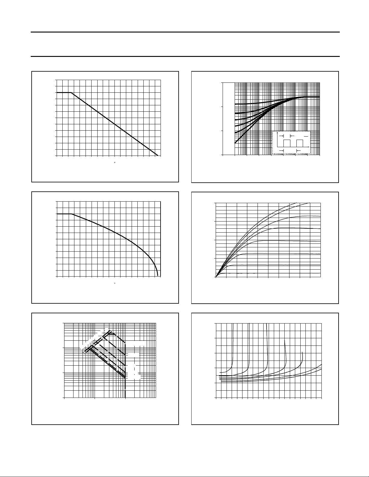
PD%
120
110
100
90
80
70
60
50
40
30
20
10
0
0 20 40 60 80 100 120 140 160 180
Normalised Power Derating
Tmb / C
Fig.1. Normalised power dissipation.
PD% = 100⋅PD/P
ID%
120
110
100
90
80
70
60
50
40
30
20
10
0
0 20 40 60 80 100 120 140 160 180
Tmb / C
= f(Tmb)
D 25 ˚C
Normalised Current Derating
Fig.2. Normalised continuous drain current.
ID% = 100⋅ID/I
= f(Tmb); conditions: VGS ≥ 5 V
D 25 ˚C
1E+01
1E+00
Zth j-mb / (K/W)
0.5
BUKX52
0.2
0.1
1E-01
0.05
0.02
p
D =
t
T
t
p
P
D
0
t
1E-02
1E-07 1E-05 1E-03 1E-01 1E+01
t / s
T
Fig.4. Transient thermal impedance.
Z
= f(t); parameter D = tp/T
th j-mb
ID / A
20
15
10
VGS / V =
5
0
0 2 4 6 8 10
10
VDS / V
BUK552-100A
7
5
4
3
Fig.5. Typical output characteristics, Tj = 25 ˚C
ID = f(VDS); parameter V
GS
.
ID / A
100
A
10
1
0.1
1 100
RDS(ON) = VDS/ID
DC
10
VDS / V
B
BUK552-100
tp = 10 us
100 us
1 ms
10 ms
100 ms
Fig.3. Safe operating area. Tmb = 25 ˚C
ID & IDM = f(VDS); IDM single pulse; parameter t
RDS(ON) / Ohm
1.0
0.8
0.6
0.4
0.2
0
0 2 4 6 8 10 12 14 16 18 20
3 3.5
4
VGS / V =
ID / A
Fig.6. Typical on-state resistance, Tj = 25 ˚C
R
p
= f(ID); parameter V
DS(ON)
BUK552-100A
4.5
5
7
10
.
GS
April 1993 3 Rev 1.100
 Loading...