

Philips BUK482-200A Datasheet

Philips Semiconductors Product specification
PowerMOS transistor BUK482-200A
GENERAL DESCRIPTION QUICK REFERENCE DATA
N-channel enhancement mode SYMBOL PARAMETER MAX. UNIT
field-effect power transistor in a
plastic envelope suitable for surface V
mounting featuring high avalanche I
energy capability, stable blocking P
voltage, fast switching and high R
thermal cycling performance.
DS
D
tot
DS(ON)
Intended for use in Switched Mode
PowerSupplies(SMPS)and general
purpose switching applications.
PINNING - SOT223 PIN CONFIGURATION SYMBOL
Drain-source voltage 200 V
Drain current (DC) 2.0 A
Total power dissipation 8.3 W
Drain-source on-state resistance 0.9 Ω
PIN DESCRIPTION
4
d
1 gate
2 drain
3 source
4 drain (tab)
1
23
g
s
LIMITING VALUES
Limiting values in accordance with the Absolute Maximum System (IEC 134)
SYMBOL PARAMETER CONDITIONS MIN. MAX. UNIT
V
V
±V
I
D
I
DM
I
DR
I
DRM
P
T
T
DS
DGR
GS
tot
stg
j
Drain-source voltage - 200 V
Drain-gate voltage RGS = 20 kΩ - 200 V
Gate-source voltage - 30 V
Drain current (DC) Tsp = 25 ˚C - 2.0 A
Tsp = 100 ˚C - 1.3 A
Drain current (pulse peak Tsp = 25 ˚C - 8.0 A
value)
Source-drain diode current Tsp = 25 ˚C - 2.0 A
(DC)
Source-drain diode current Tsp = 25 ˚C - 8.0 A
(pulse peak value)
Total power dissipation Tsp = 25 ˚C - 8.3 W
Storage temperature -55 150 ˚C
Junction Temperature - 150 ˚C
AVALANCHE LIMITING VALUE
SYMBOL PARAMETER CONDITIONS MIN. MAX. UNIT
W
DSS
January 1998 1 Rev 1.000
Drain-source non-repetitive ID = 2 A ; VDD ≤ 50 V ; VGS = 10 V ;
unclamped inductive turn-off RGS = 50 Ω
energy Tj = 25˚C prior to surge - 50 mJ
Tj = 100˚C prior to surge - 8 mJ

Philips Semiconductors Product specification
PowerMOS transistor BUK482-200A
THERMAL RESISTANCES
SYMBOL PARAMETER CONDITIONS MIN. TYP. MAX. UNIT
R
th j-sp
R
th j-a
STATIC CHARACTERISTICS
Tj = 25 ˚C unless otherwise specified
SYMBOL PARAMETER CONDITIONS MIN. TYP. MAX. UNIT
V
(BR)DSS
V
GS(TO)
I
DSS
I
GSS
R
DS(ON)
V
SD
Thermal resistance junction to - - 15 K/W
solder point
Thermal resistance junction to pcb mounted; minimum footprint - 156 - K/W
ambient pcb mounted; pad area as in fig:17 - 70 - K/W
Drain-source breakdown VGS = 0 V; ID = 0.25 mA 200 - - V
voltage
Gate threshold voltage VDS = VGS; ID = 0.25 mA 2.0 3.0 4.0 V
Zero gate voltage drain current VDS = 200 V; VGS = 0 V; Tj = 25 ˚C - 0.1 10 µA
VDS = 200 V; VGS = 0 V; Tj = 125 ˚C - 0.1 1.0 mA
Gate source leakage current VGS = ±30 V; VDS = 0 V - 10 100 nA
Drain-source on-state VGS = 10 V; ID = 2 A - 0.53 0.9 Ω
resistance
Source-drain diode forward IF = 2 A ;VGS = 0 V - 0.87 1.0 V
voltage
DYNAMIC CHARACTERISTICS
Tj = 25 ˚C unless otherwise specified
SYMBOL PARAMETER CONDITIONS MIN. TYP. MAX. UNIT
g
C
C
C
Q
Q
Q
t
t
t
t
t
Q
fs
iss
oss
rss
g(tot)
gs
gd
d on
r
d off
f
rr
rr
Forward transconductance VDS = 25 V; ID = 2 A 0.5 2.6 - S
Input capacitance VGS = 0 V; VDS = 25 V; f = 1 MHz - 305 400 pF
Output capacitance - 60 100 pF
Feedback capacitance - 24 50 pF
Total gate charge VGS = 10 V; ID = 2 A; V
Gate to source charge - 2 - nC
= 160 V - 13 - nC
DS
Gate to drain (Miller) charge - 5 - nC
Turn-on delay time VDD = 30 V; ID = 2.75 A; - 10 15 ns
Turn-on rise time VGS = 10 V; RGS = 50 Ω; - 30 45 ns
Turn-off delay time R
Turn-off fall time - 20 30 ns
= 50 Ω - 3040ns
GEN
Source-drain diode reverse IF = 2 A; -dIF/dt = 100 A/µs; - 88 - ns
recovery time
Source-drain diode reverse VGS = 0 V; VR = 100 V - 370 - nC
recovery charge
January 1998 2 Rev 1.000
Philips Semiconductors Product specification
PowerMOS transistor BUK482-200A
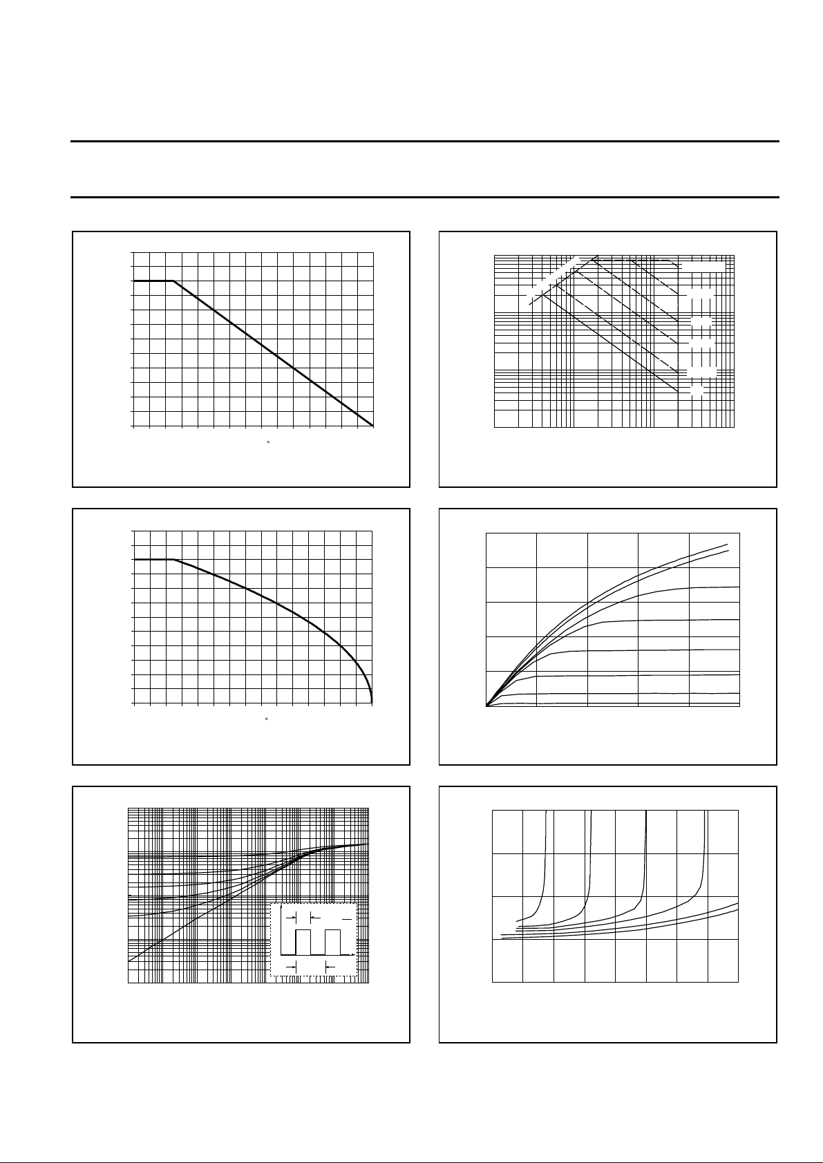
PD%
120
110
100
90
80
70
60
50
40
30
20
10
0
0 20 40 60 80 100 120 140
Normalised Power Derating
Tamb / C
Fig.1. Normalised power dissipation.
PD% = 100⋅PD/P
ID%
120
110
100
90
80
70
60
50
40
30
20
10
0
0 20 40 60 80 100 120 140
Tamb / C
= f(T
D 25 ˚C
Normalised Current Derating
amb
)
Fig.2. Normalised continuous drain current.
ID% = 100⋅ID/I
D 25 ˚C
= f(T
); conditions: VGS ≥ 10 V
amb
ID / A
10
RDS(ON) = VDS/ID
1
0.1
0.01
1 10 100 1000
Fig.4. Safe operating area. T
ID & IDM = f(VDS); IDM single pulse; parameter t
ID / A
10
8
6
4
2
0
0246810
BUK482-200A
VDS / V
BUK482-200A
VDS / V
tp = 10 us
100 us
1 ms
10 ms
100 ms
DC
= 25 ˚C.
amb
VGS = 20 V
10
6.5
6
5.5
5
4.5
4
Fig.5. Typical output characteristics, Tj = 25 ˚C
ID = f(VDS); parameter V
GS
p
.
Zth(j-sp) K/W
100
10
1
0.1
0.01
1us 10us 100us 1ms 10ms 100ms 1s 10s
Fig.3. Transient thermal impedance.
Z
= f(t); parameter D = tp/T
th j-sp
BUK482-200A
tp / sec
RDS(ON) / Ohms
2
1.5
VGS =
1
t
t
p
P
D
p
D =
T
t
T
0.5
0
5 V 5.5 V
012345678
Fig.6. Typical on-state resistance, Tj = 25 ˚C
R
DS(ON)
BUK482-200A
6 V
ID / A
= f(ID); parameter V
6.5 V
10 V
20 V
.
GS
January 1998 3 Rev 1.000
 Loading...