

Philips BUK221-50DY Technical data

查询BUK221-50DY供应商
1. Product profile
1.1 Description
Monolithic temperature and overload protected dual high-side powerswitch based on
TOPFET™ Trench technology in a 7-pin surface mount plastic package.
Product availability:
BUK221-50DY
Dual channel high-side TOPFET™
Rev. 01 — 16 April 2003 Product data
BUK221-50DY in SOT427 (D2-PAK).
1.2 Features
■ Very low quiescent current ■ CMOS logic compatibility
■ Power TrenchMOS™ ■ Current limitation
■ Overtemperature protection ■ Latched overload protection
■ Over and undervoltage protection ■ ESD protection for all pins
■ Reverse battery protection ■ Diagnostic status indication
■ Low charge pump noise ■ Off-state open load detection
■ Loss of ground protection ■ Load dump protection
■ Negative load clamping ■ Internal ground resistor.
1.3 Applications
■ 12 and 24 V grounded loads ■ High inrush current loads
■ Inductive loads ■ Replacement for relays and fuses.
1.4 Quick reference data
Table 1: Quick reference data
Symbol Parameter Min Max Units
R
BLon
I
L
I
L(nom)
I
L(lim)
V
BG(oper)
battery-load on-state resistance - 90 mΩ
load current - 4 A
nominal load current (ISO) 3.6 - A
self-limiting load current 8 16 A
battery-ground operating voltage 5.5 35 V
Philips Semiconductors
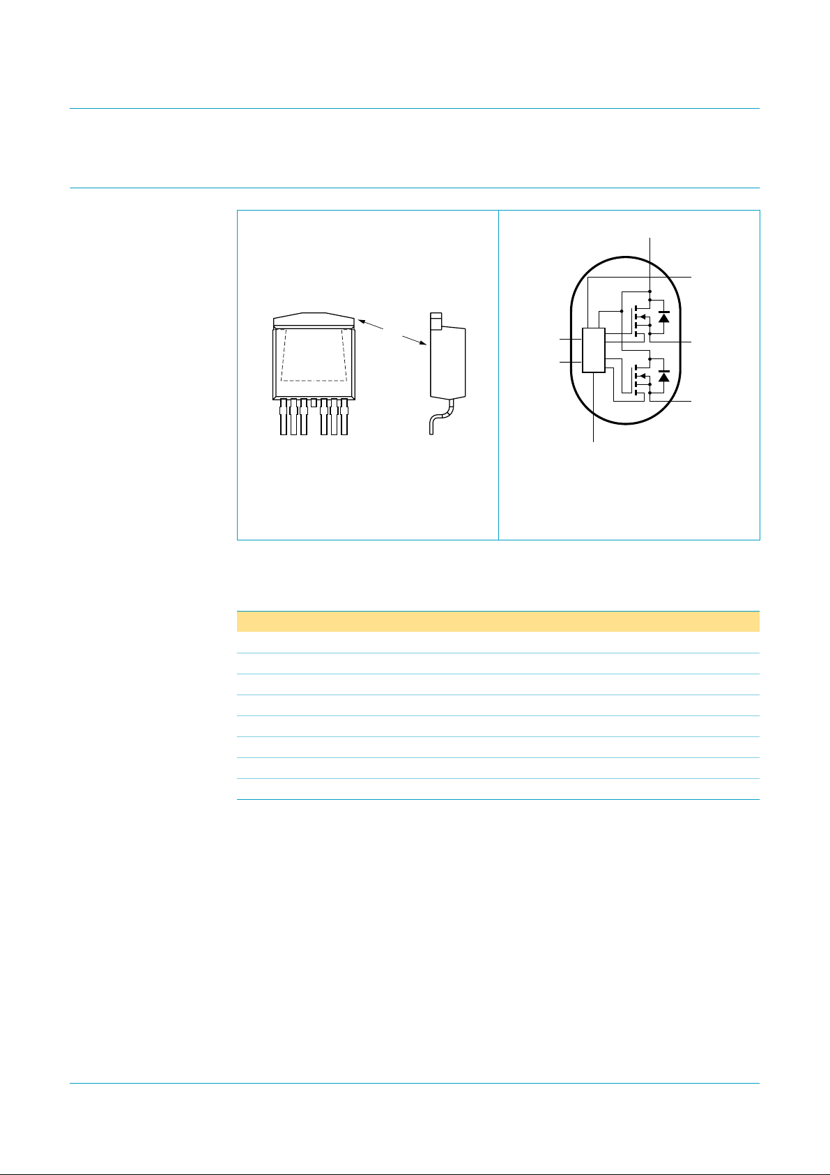
2. Pinning information
BUK221-50DY
Dual channel high-side TOPFET™
B
S
mb
1234567
Front view
No connection can be made to pin 4
(cropped).
MBK128
I1
I2
P represents protection circuitry.
Fig 1. Pinning; SOT427 (D2-PAK). Fig 2. Symbol; (Dual High-Side Switch)
TOPFET
2.1 Pin description
Table 2: Pin description
Symbol Pin I/O Description
L1 1 O load 1
G 2 - circuit common ground
I1 3 I input 1
B4-
[1] [2]
S 5 O status
I2 6 I input 2
L2 7 O load 2
-mb-
[2]
battery
mounting base
P
G
TM
.
L1
L2
03pa68
[1] Pin 4 is cropped and cannot be connected to the PCB by surface mounting.
[2] The battery is connected to the mounting base.
9397 750 11167
Product data Rev. 01 — 16 April 2003 2 of 16
© Koninklijke Philips Electronics N.V. 2003. All rights reserved.
Philips Semiconductors
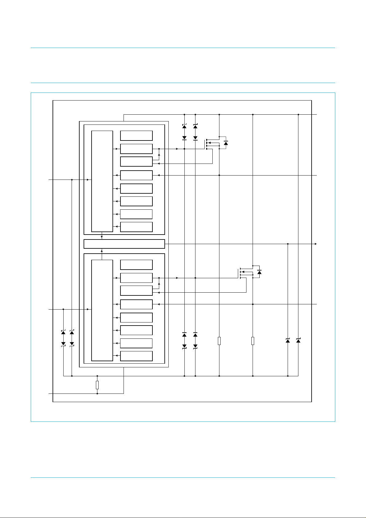
3. Block diagram
BUK221-50DY
Dual channel high-side TOPFET™
BUK221-50DY
4/mb
B
CHANNEL1
VOLTAGE
REGULATOR
CHARGE PUMP
CURRENT LIMIT
3
I1
CONTROL
LOGIC1
STATUS DIAGNOSIS
OPEN CIRCUIT
OVERVOLTAGE
PROTECTION
UNDERVOLTAGE
PROTECTION
SHORT CIRCUIT
PROTECTION
TEMPERATURE
CHANNEL2
REGULATOR
CHARGE PUMP
SENSOR
SENSOR
VOLTAGE
POWER
MOSFET1
POWER
MOSFET2
1
L1
5
S
CURRENT LIMIT
OPEN CIRCUIT
6
I2
2
G
CONTROL
LOGIC2
R
G
SENSOR
OVERVOLTAGE
PROTECTION
UNDERVOLTAGE
PROTECTION
SHORT CIRCUIT
PROTECTION
TEMPERATURE
SENSOR
Fig 3. Elements of the dual high-side TOPFET switch.
7
L2
R
LG1
R
LG2
03pa69
9397 750 11167
© Koninklijke Philips Electronics N.V. 2003. All rights reserved.
Product data Rev. 01 — 16 April 2003 3 of 16

Philips Semiconductors
BUK221-50DY
Dual channel high-side TOPFET™
4. Functional description
A diagnostic status ensures faster fault detection.
Active current limit is combined with latched short circuit protection in order to
protect the device in the event of a short circuit.
Thermal shutdown for high temperature conditions has an automatic restart at a
lower temperature so providing protection against excessive power dissipation.
Active clamping protects the device against low energy spikes.
Undervoltage lockout means the device shuts down for low battery voltages, thus
avoiding faulty operation.
Overvoltage shutdown in the on-state protects a load such as a lamp filament from
potentially destructive voltage spikes.
Table 3: Truth table
Abbreviations: L = logic LOW; H = logic HIGH; X = don’t care; 0 = condition not present; 1 = condition present;
UV = undervoltage; OV = overvoltage; OC = open circuit load; SC = short circuit; OT = overtemperature
Input Supply Load 1 Load 2 Load output Status Operating mode
1 2 UV OV OC SC OT OC SC OT 1 2
L L 0 X 0 X X 0 X X OFF OFF H both off & normal
LL0X1XXXXXOFFOFF Lboth off, one/both OC or
shorted to V
Figure 10
L H 0 X 1 X X 0 0 0 OFF ON L one off & OC, with other on
& normal
HL00000000ONOFFHone on & normal, with other
off & normal
HH00000000ONON Hboth on & normal
H X 1 0 X X X 0 X X OFF OFF H supply undervoltage lockout
H X 0 1 X 0 0 X 0 0 OFF OFF H supply overvoltage
shutdown
HX0001XXXXOFFX Lone SC tripped
HL0001X00XOFFOFFLone SC tripped, with other
off & normal
HH0001X000OFFON Lone SC tripped, with other
on & normal
HX00001XXXOFFX Lone OT shutdown
HL0000100XOFFOFFLoneOTshutdown,with other
off & normal
HH00001000OFFON LoneOTshutdown,with other
on & normal
[1]
.
or battery;
S
[1] The status will continue to indicate OT (even if the input goes LOW) until the device cools below the reset threshold temperature.
See “Overtemperature protection” characteristics in Table 6 “Static characteristics”.
9397 750 11167
Product data Rev. 01 — 16 April 2003 4 of 16
© Koninklijke Philips Electronics N.V. 2003. All rights reserved.

Philips Semiconductors
BUK221-50DY
Dual channel high-side TOPFET™
5. Limiting values
Table 4: Limiting values
In accordance with the Absolute Maximum Rating System (IEC 60134).
Symbol Parameter Conditions Min Max Unit
V
BG
I
L
P
tot
T
stg
T
j
T
mb
battery-ground supply voltage
load current Tmb≤ 130 °C-4A
total power dissipation Tmb≤ 25 °C - 44.6 W
storage temperature −55 +175 °C
junction temperature −40 +150 °C
mounting base temperature during soldering (≤ 10 s) - 260 °C
Reverse battery voltage
V
V
BGR
BGRR
reverse battery-ground supply voltage RI≥ 3.3 kΩ; RSS≥ 3.3 kΩ; Figure 10
repetitive reverse battery-ground
supply voltage
Input current
I
I
I
IRM
input current −5+5mA
repetitive peak input current δ≤0.1; tp= 300 µs −50 +50 mA
Status current
I
S
I
SRM
status current −5+5mA
repetitive peak status current δ≤0.1; tp= 300 µs −50 +50 mA
Inductive load clamping
E
BL(CL)S
non-repetitive battery-load clamping
energy
Electrostatic discharge voltage
V
esd
electrostatic discharge voltage Human Body Model 1; C = 100 pF;
Tj= 150 °C prior to turn-off; VBG=13V;
= 5 A; (one channel) Figure 13
I
L
R = 1.5 kΩ
[1]
-45V
[2]
-16V
-32V
-60mJ
-2kV
[1] The device will not be harmed by exposure to the maximum supply voltage, but normal operation is not possible because of overvoltage
shutdown - see Table 6 “Static characteristics” for the operating range.
[2] Reverse battery voltage is only allowed with external resistors to limit the input and status currents to a safe value. The connected load
must limit the reverse load current. The internal ground resistor limits the reverse battery ground current. See Figure 10 “Typical
dynamic response circuit diagram including reverse supply protection and open load detection.”
6. Thermal characteristics
Table 5: Thermal characteristics
Symbol Parameter Conditions Min Typ Max Unit
R
th(j-mb)
thermal resistance from junction to
mounting base
R
th(j-a)
thermal resistance from junction to
ambient
9397 750 11167
Product data Rev. 01 — 16 April 2003 5 of 16
per channel - 4 5.6 K/W
both channels - 2 2.8 K/W
mounted on printed circuit board;
- 50 - K/W
minimum footprint
© Koninklijke Philips Electronics N.V. 2003. All rights reserved.
 Loading...