

Philips BUK210-50Y, BUK215-50Y User Manual
Philips Semiconductors Product specification
TOPFET high side switch BUK215-50Y
SMD version of BUK210-50Y
DESCRIPTION QUICK REFERENCE DATA
Monolithic single channel high side SYMBOL PARAMETER MIN. UNIT
protected power switch in
TOPFET2 technology assembled in I
a 5 pin plastic surface mount
L
package.
SYMBOL PARAMETER MAX. UNIT
APPLICATIONS
V
General controller for driving I
lamps, motors, solenoids, heaters. T
BG
L
j
R
ON
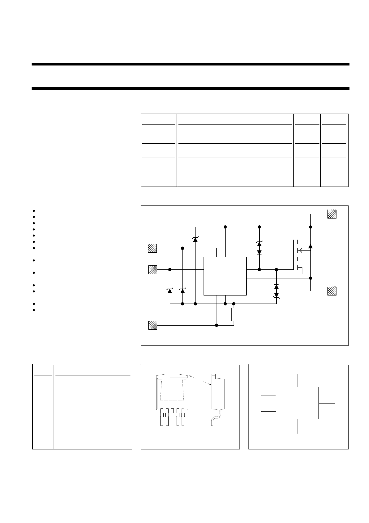
FEATURES FUNCTIONAL BLOCK DIAGRAM
Vertical power TrenchMOS
Low on-state resistance
CMOS logic compatible
Very low quiescent current
Overtemperature protection
Load current limiting
Latched overload and
short circuit protection
Overvoltage and undervoltage
shutdown with hysteresis
On-state open circuit load
detection
Diagnostic status indication
Voltage clamping for turn off
of inductive loads
ESD protection on all pins
Reverse battery, overvoltage
and transient protection
STATUS
INPUT
GROUND
Nominal load current (ISO) 9 A
Continuous off-state supply voltage 50 V
Continuous load current 20 A
Continuous junction temperature 150 ˚C
On-state resistance Tj = 25˚C 38 mΩ
BATT
POWER
MOSFET
CONTROL &
PROTECTION
CIRCUITS
LOAD
RG
Fig.1. Elements of the TOPFET HSS with internal ground resistor.
PINNING - SOT426 PIN CONFIGURATION SYMBOL
PIN DESCRIPTION
1 Ground
2 Input
3 (connected to mb)
4 Status
5 Load
3
12 45
mb Battery
May 2001 1 Rev 1.010
mb
B
I
TOPFET
HSS
S
Fig. 2. Fig. 3.
G
L

Philips Semiconductors Product specification
TOPFET high side switch BUK215-50Y
SMD version of BUK210-50Y
LIMITING VALUES
Limiting values in accordance with the Absolute Maximum System (IEC 134)
SYMBOL PARAMETER CONDITIONS MIN. MAX. UNIT
V
BG
I
L
P
D
T
stg
T
j
T
sold
-V
BG
-V
BG
RI, R
II, I
S
II, I
S
E
BL
Continuous supply voltage 0 50 V
Continuous load current T
Total power dissipation T
95˚C - 20 A
mb ≤
25˚C - 67 W
mb ≤
Storage temperature -55 175 ˚C
Continuous junction temperature
1
- 150 ˚C
Mounting base temperature during soldering - 260 ˚C
Reverse battery voltages
2
Continuous reverse voltage - 16 V
Peak reverse voltage - 32 V
Application information
S
External resistors
3
to limit input, status currents 3.2 - kΩ
Input and status
Continuous currents -5 5 mA
Repetitive peak currents δ ≤ 0.1, tp = 300 µs -50 50 mA
Inductive load clamping IL = 10 A, VBG = 16 V
Non-repetitive clamping energy Tj ≤ 150˚C prior to turn-off - 150 mJ
ESD LIMITING VALUE
SYMBOL PARAMETER CONDITIONS MIN. MAX. UNIT
V
C
Electrostatic discharge capacitor Human body model; - 2 kV
voltage C = 250 pF; R = 1.5 kΩ
THERMAL CHARACTERISTICS
SYMBOL PARAMETER CONDITIONS MIN. TYP. MAX. UNIT
Thermal resistance
R
th j-mb
1 For normal continuous operation. A higher Tj is allowed as an overload condition but at the threshold T
2 Reverse battery voltage is allowed only with external resistors to limit the input and status currents to a safe value. The connected load must
3 To limit currents during reverse battery and transient overvoltages (positive or negative).
4 Of the output power MOS transistor.
Junction to mounting base - - 1.52 1.86 K/W
to protect the switch.
limit the reverse load current. The internal ground resistor limits the reverse battery ground current. Power is dissipated and the T
rating must be observed.
4
the over temperature trip operates
j(TO)
j
May 2001 2 Rev 1.010

Philips Semiconductors Product specification
TOPFET high side switch BUK215-50Y
SMD version of BUK210-50Y
STATIC CHARACTERISTICS
Limits are at -40˚C ≤ Tmb ≤ 150˚C and typicals at Tmb = 25 ˚C unless otherwise stated.
SYMBOL PARAMETER CONDITIONS MIN. TYP. MAX. UNIT
Clamping voltages
V
V
-V
-V
V
I
I
I
I
BG
BL
LG
LG
BG
B
L
G
L
Battery to ground IG = 1 mA 50 55 65 V
Battery to load IL = IG = 1 mA 50 55 65 V
Negative load to ground IL = 10 mA 18 23 28 V
Negative load voltage
1
IL = 10 A; tp = 300 µs202530V
Supply voltage battery to ground
Operating range
2
5.5 - 35 V
Currents 9 V ≤ VBG ≤ 16 V
Quiescent current
3
VLG = 0 V - - 20 µA
Tmb = 25˚C - 0.1 2 µA
Off-state load current
4
VBL = V
BG
--20µA
Tmb = 25˚C - 0.1 1 µA
Operating current
Nominal load current
Resistances V
5
6
IL = 0 A - 2 4 mA
VBL = 0.5 V Tmb = 85˚C 9 - - A
BG
I
L
7
t
p
T
mb
R
ON
On-state resistance 9 to 35 V 10 A 300 µs 25˚C - 28 38 mΩ
150˚C - - 70 mΩ
R
ON
On-state resistance 6 V 10 A 300 µs 25˚C - 36 48 mΩ
150˚C - - 88 mΩ
R
G
1 For a high side switch, the load pin voltage goes negative with respect to ground during the turn-off of an inductive load.
2 On-state resistance is increased if the supply voltage is less than 9 V.
3 This is the continuous current drawn from the supply when the input is low and includes leakage current to the load.
4 The measured current is in the load pin only.
5 This is the continuous current drawn from the supply with no load connected, but with the input high.
6 Defined as in ISO 10483-1. For comparison purposes only. This parameter will not be characterised for automotive PPAP.
7 The supply and input voltage for the RON tests are continuous. The specified pulse duration tp refers only to the applied load current.
Internal ground resistance IG = 10 mA 95 150 190 Ω
May 2001 3 Rev 1.010

Philips Semiconductors Product specification
TOPFET high side switch BUK215-50Y
SMD version of BUK210-50Y
INPUT CHARACTERISTICS
9 V ≤ VBG ≤ 16 V. Limits are at -40˚C ≤ Tmb ≤ 150˚C and typicals at Tmb = 25 ˚C unless otherwise stated.
SYMBOL PARAMETER CONDITIONS MIN. TYP. MAX. UNIT
I
I
V
IG
V
IG(ON)
V
IG(OFF)
∆V
I
I(ON)
I
I(OFF)
IG
Input current VIG = 5 V 20 90 160 µA
Input clamping voltage II = 200 µA 5.5 7 8.5 V
Input turn-on threshold voltage - 2.4 3 V
Input turn-off threshold voltage 1.5 2.1 - V
Input turn-on hysteresis - 0.3 - V
Input turn-on current VIG = 3 V - - 100 µA
Input turn-off current VIG = 1.5 V 10 - - µA
STATUS CHARACTERISTICS
The status output is an open drain transistor, and requires an external pull-up circuit to indicate a logic high.
Limits are at -40˚C ≤ Tmb ≤ 150˚C and typicals at Tmb = 25 ˚C unless otherwise stated. Refer to TRUTH TABLE.
SYMBOL PARAMETER CONDITIONS MIN. TYP. MAX. UNIT
V
SG
V
SG
I
S
I
S
Status clamping voltage IS = 100 µA 5.5 7 8.5 V
Status low voltage IS = 100 µA--1V
Tmb = 25˚C - 0.7 0.8 V
Status leakage current VSG = 5 V - - 15 µA
Tmb = 25˚C - 0.1 1 µA
Status saturation current
1
VSG = 5 V 2 7 12 mA
Application information
R
S
External pull-up resistor - 47 - kΩ
OPEN CIRCUIT DETECTION CHARACTERISTICS
An open circuit load can be detected in the on-state. Refer to TRUTH TABLE.
Limits are at -40˚C ≤ Tmb ≤ 150˚C and typical is at Tmb = 25 ˚C.
SYMBOL PARAMETER CONDITIONS MIN. TYP. MAX. UNIT
Open circuit detection 9 V ≤ VBG ≤ 35 V
I
L(TO)
∆I
L(TO)
1 In a fault condition with the pull-up resistor short circuited while the status transistor is conducting. This condition should be avoided in order to
May 2001 4 Rev 1.010
Low current detect threshold 0.24 - 1.6 A
Tj = 25˚C 0.4 0.8 1.2 A
Hysteresis - 0.16 - A
prevent possible interference with normal operation of the device.
 Loading...