

Philips BUK138-50DL Technical data
查询BUK138-50DL供应商查询BUK138-50DL供应商
Philips Semiconductors Product specification
Logic level TOPFET BUK138-50DL
D-PAK version of BUK117-50DL
DESCRIPTION QUICK REFERENCE DATA
Monolithic temperature and SYMBOL PARAMETER MAX. UNIT
overload protected logic level power
MOSFET in TOPFET2 technology V
assembled in a 3 pin surface mount I
plastic package. P
APPLICATIONS R
D
T
DS
D
j
DS(ON)
Continuous drain source voltage 50 V
Continuous drain current 8 A
Total power dissipation 40 W
Continuous junction temperature 150 ˚C
Drain-source on-state resistance 100 mΩ
General purpose switch for driving I
lamps
ISL
Input supply current VIS = 5 V 650 µA
motors
solenoids
heaters
in automotive systems and other
applications.
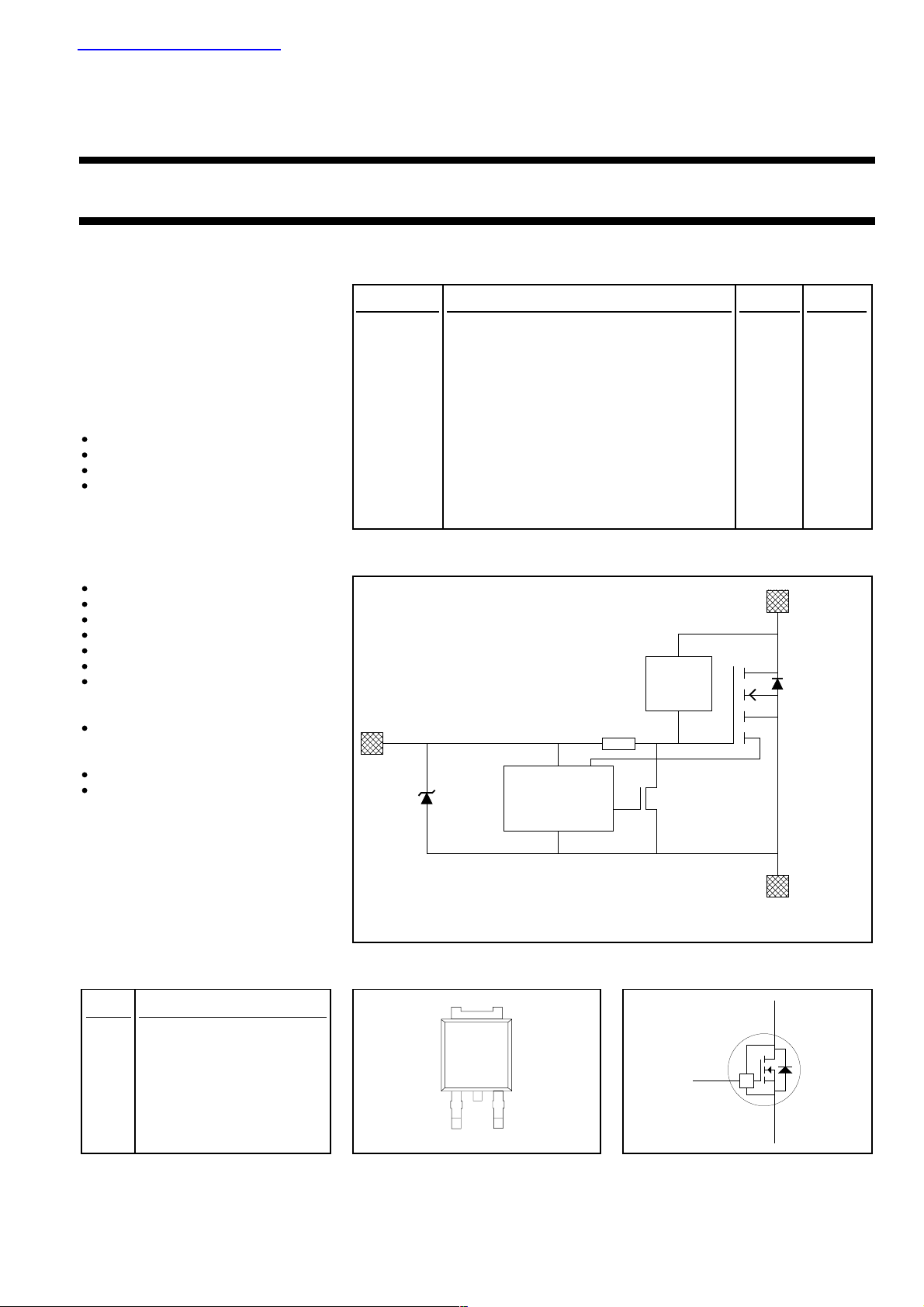
FEATURES FUNCTIONAL BLOCK DIAGRAM
TrenchMOS output stage
Current limiting
Overload protection
Overtemperature protection
Protection latched reset by input
5 V logic compatible input level
Control of output stage and
supply of overload protection
circuits derived from input
Low operating input current
permits direct drive by
micro-controller
ESD protection on all pins
Overvoltage clamping for turn
off of inductive loads
INPUT
RIG
LOGIC AND
PROTECTION
O / V
CLAMP
DRAIN
POWER
MOSFET
SOURCE
Fig.1. Elements of the TOPFET.
PINNING - SOT428 PIN CONFIGURATION SYMBOL
PIN DESCRIPTION
1 input
2 drain
3 source
tab drain
May 2001 1 Rev 1.300
tab
TOPFET
I
2
1
3
D
P
S
Philips Semiconductors Product specification
Logic level TOPFET BUK138-50DL
D-PAK version of BUK117-50DL
LIMITING VALUES
Limiting values in accordance with the Absolute Maximum Rating System (IEC 134)
SYMBOL PARAMETER CONDITIONS MIN. MAX. UNIT
V
I
I
I
I
P
T
T
T
DS
D
D
I
IRM
D
stg
j
sold
Continuous drain source voltage
Continuous drain current VIS = 5 V; T
Continuous drain current VIS = 5 V; T
Continuous input current - -5 5 mA
Non-repetitive peak input current tp ≤ 1 ms -10 10 mA
Total power dissipation Tmb ≤ 25 ˚C - 40 W
Storage temperature - -55 175 ˚C
Continuous junction temperature
Case temperature during soldering - 260 ˚C
ESD LIMITING VALUE
SYMBOL PARAMETER CONDITIONS MIN. MAX. UNIT
1
- - 50 V
25 ˚C - self - A
mb =
limited
110 ˚C - 8 A
mb ≤
2
normal operation - 150 ˚C
V
C
Electrostatic discharge capacitor Human body model; - 2 kV
voltage C = 250 pF; R = 1.5 kΩ
OVERVOLTAGE CLAMPING LIMITING VALUES
At a drain source voltage above 50 V the power MOSFET is actively turned on to clamp overvoltage transients.
SYMBOL PARAMETER CONDITIONS MIN. MAX. UNIT
Inductive load turn-off IDM = 8 A; VDD ≤ 20 V
E
DSM
E
DRM
Non-repetitive clamping energy Tmb ≤ 25 ˚C - 100 mJ
Repetitive clamping energy Tmb ≤ 95 ˚C; f = 250 Hz - 20 mJ
OVERLOAD PROTECTION LIMITING VALUE
With an adequate protection supply provided via the input pin, TOPFET can protect itself from two types of overload
- overtemperature and short circuit load.
SYMBOL PARAMETER REQUIRED CONDITION MIN. MAX. UNIT
V
DS
Drain source voltage
3
4 V ≤ VIS ≤ 5.5 V 0 35 V
THERMAL CHARACTERISTIC
SYMBOL PARAMETER CONDITIONS MIN. TYP. MAX. UNIT
Thermal resistance
R
R
th j-mb
th j-a
Junction to mounting base - - 2.5 3.1 K/W
Junction to ambient minimum footprint FR4 PCB - 71.4 - K/W
1 Prior to the onset of overvoltage clamping. For voltages above this value, safe operation is limited by the overvoltage clamping energy.
2 A higher Tj is allowed as an overload condition but at the threshold T
3 All control logic and protection functions are disabled during conduction of the source drain diode.
the over temperature trip operates to protect the switch.
j(TO)
May 2001 2 Rev 1.300
 Loading...