

Philips BUK136-50L Technical data
查询BUK136-50L供应商查询BUK136-50L供应商
Philips Semiconductors Product specification
Logic level TOPFET BUK136-50L
SMD version of BUK125-50L
DESCRIPTION QUICK REFERENCE DATA
Monolithic logic level protected SYMBOL PARAMETER MAX. UNIT
power MOSFET using TOPFET2
technology assembled in a 5 pin V
surface mounting plastic package. I
APPLICATIONS T
General purpose switch for
D
P
R
DS
tot
j
DS(ON)
automotive systems and other SYMBOL PARAMETER NOM. UNIT
applications.
V
PS
Continuous drain source voltage 50 V
Continuous drain current 40 A
Total power dissipation 107 W
Continuous junction temperature 150 ˚C
Drain-source on-state resistance 20 mΩ
Protection supply voltage 5 V
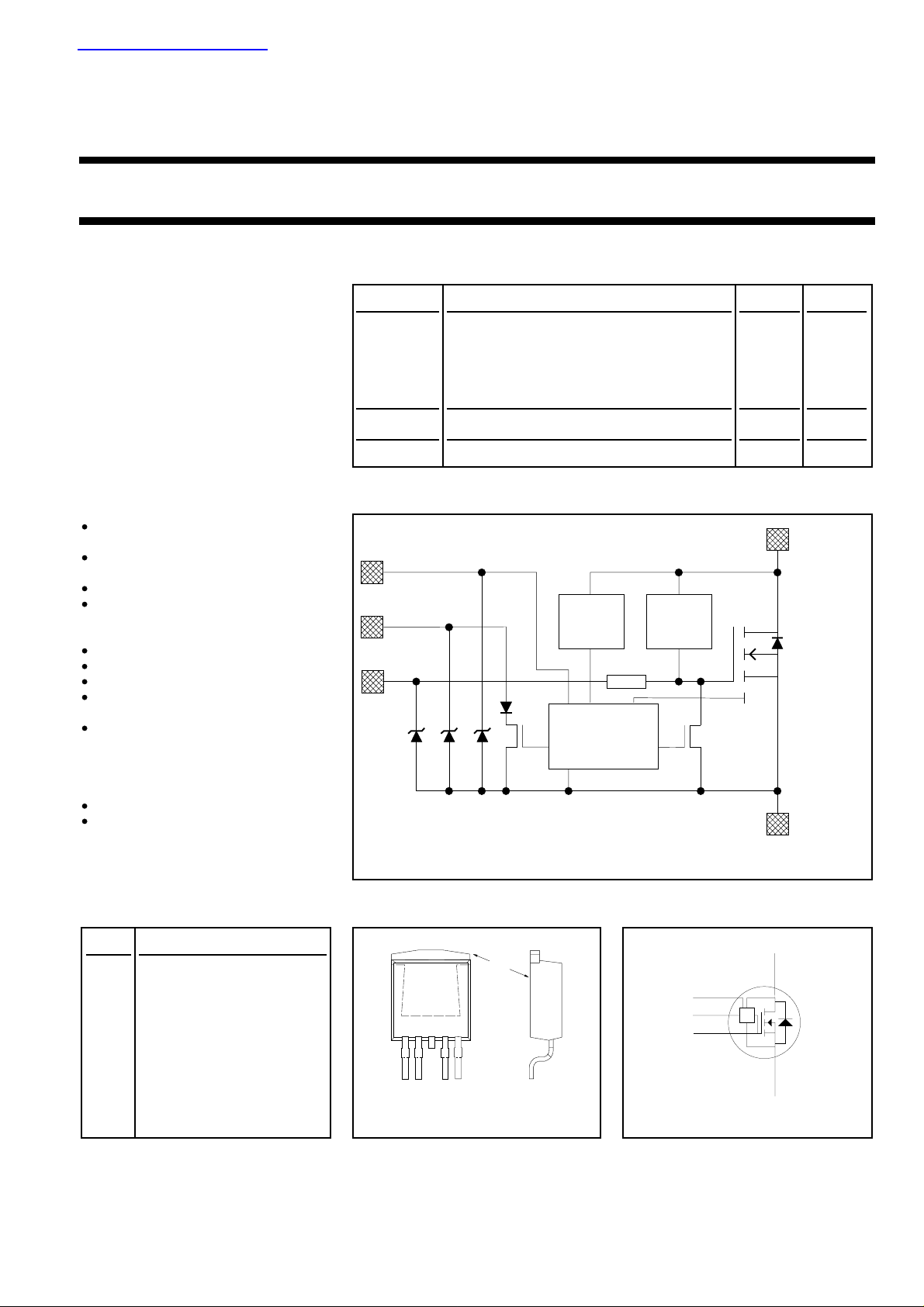
FEATURES FUNCTIONAL BLOCK DIAGRAM
TrenchMOS output stage with
low on-state resistance
PROTECTION SUPPLY
Separate input pin for higher
frequency drive
5 V logic compatible input
Separate supply pin for logic
and protection circuits with low
operating current
Overtemperature protection
Drain current limiting
FLAG
INPUT
OC LOAD
DETECT
O/V
CLAMP
RIG
Short circuit load protection
Latched overload trip state reset
by the protection pin
Diagnostic flag pin indicates
protection supply connected,
LOGIC AND
PROTECTION
overtemperature condition,overload
tripped state, or open circuit load
(detected in the off-state)
ESD protection on all pins
Overvoltage clamping
Fig.1. Elements of the TOPFET.
PINNING - SOT426 PIN CONFIGURATION SYMBOL
PIN DESCRIPTION
1 input
2 flag
3 (connected to mb)
4 protection supply
5 source
mb drain
3
12 45
mb
Fig. 2. Fig. 3.
TOPFET
P
F
I
DRAIN
POWER
MOSFET
SOURCE
D
P
S
July 2002 1 Rev 1.000

Philips Semiconductors Product specification
Logic level TOPFET BUK136-50L
SMD version of BUK125-50L
LIMITING VALUES
Limiting values in accordance with the Absolute Maximum Rating System (IEC 134)
SYMBOL PARAMETER CONDITIONS MIN. MAX. UNIT
Continuous voltage
V
DS
Drain source voltage
Continuous currents
I
D
I
I
I
F
I
P
Drain current VPS = 5 V; T
Input current -5 5 mA
Flag current -5 5 mA
Protection supply current -5 5 mA
Thermal
P
tot
T
stg
T
j
T
sold
Total power dissipation Tmb = 25˚C - 107 W
Storage temperature -55 175 ˚C
Junction temperature
Mounting base temperature during soldering - 260 ˚C
1
2
VIS = 0 V - 50 V
25˚C - self - A
VPS = 0 V; T
mb =
80˚C - 40 A
mb =
limited
continuous - 150 ˚C
ESD LIMITING VALUE
SYMBOL PARAMETER CONDITIONS MIN. MAX. UNIT
V
C
Electrostatic discharge capacitor Human body model; - 2 kV
voltage C = 250 pF; R = 1.5 kΩ
OVERLOAD PROTECTION LIMITING VALUE
With an adequate protection supply For overload conditions an n-MOS The drain current is limited to
connected, TOPFET can protect transistor turns on between the reduce dissipation in case of short
itself from two types of overload - input and source to quickly circuit load. Refer to OVERLOAD
overtemperature and short circuit discharge the power MOSFET CHARACTERISTICS.
load. gate capacitance.
SYMBOL PARAMETER REQUIRED CONDITION MIN. MAX. UNIT
Overload protection
V
DS
Drain source voltage VPS ≥ 4 V 0 35 V
3
protection supply
OVERVOLTAGE CLAMPING LIMITING VALUES
At a drain source voltage above 50 V the power MOSFET is actively turned on to clamp overvoltage transients.
SYMBOL PARAMETER CONDITIONS MIN. MAX. UNIT
Inductive load turn off IDM = 25 A; VDD ≤ 20 V
E
DSM
E
DRM
Non-repetitive clamping energy Tmb = 25˚C - 550 mJ
Repetitive clamping energy Tmb ≤ 95˚C; f = 250 Hz - 60 mJ
1 Prior to the onset of overvoltage clamping. For voltages above this value, safe operation is limited by the overvoltage clamping energy.
2 A higher Tj is allowed as an overload condition but at the threshold T
3 All control logic and protection functions are disabled during conduction of the source drain diode. If the protection circuit was previously
latched, it would be reset by this condition.
the over temperature trip operates to protect the switch.
j(TO)
July 2002 2 Rev 1.000

Philips Semiconductors Product specification
Logic level TOPFET BUK136-50L
SMD version of BUK125-50L
THERMAL CHARACTERISTIC
SYMBOL PARAMETER CONDITIONS MIN. TYP. MAX. UNIT
Thermal resistance
R
th j-mb
OUTPUT CHARACTERISTICS
Limits are for -40˚C ≤ Tmb ≤ 150˚C; typicals are for Tmb = 25˚C unless otherwise specified.
SYMBOL PARAMETER CONDITIONS MIN. TYP. MAX. UNIT
V
(CL)DSS
I
DSS
Junction to mounting base - - 0.94 1.17 K/W
Off-state VIS = 0 V
Drain-source clamping voltage ID = 10 mA 50 - 70 V
= 5 A; tp ≤ 300 µs; δ ≤ 0.01 50 60 70 V
I
DM
Drain source leakage current1VPS = 0 V; VDS = 40 V - - 100 µA
Tmb = 25˚C - 0.1 10 µA
On-state tp ≤ 300 µs; δ ≤ 0.01; VPS ≥ 4 V
R
DS(ON)
Drain-source resistance IDM = 15 A; VIS ≥ 4.4 V - - 40 mΩ
Tmb = 25˚C - 15 20 mΩ
INPUT CHARACTERISTICS
Limits are for -40˚C ≤ Tmb ≤ 150˚C; typicals are for Tmb = 25˚C unless otherwise specified.
SYMBOL PARAMETER CONDITIONS MIN. TYP. MAX. UNIT
Normal operation
V
I
IS
V
R
I
ISL
IS(TO)
(CL)IS
IG
Input threshold voltage
Input current VIS = 5 V - 16 100 µA
Input clamping voltage II = 1 mA 5.5 6.4 8.5 V
Internal series resistance
Overload protection latched VPS ≥ 4 V
Input current VIS = 5 V 1 2.7 4 mA
2
ID = 1 mA 0.6 - 2.6 V
Tmb = 25˚C 1.1 1.6 2.1 V
3
to gate of power MOSFET - 1.7 - kΩ
1 The drain current required for open circuit load detection is switched off when there is no protection supply, in order to ensure a low off-state
2 The measurement method is simplified if VPS = 0 V, in order to distinguish ID from I
3 This is not a directly measurable parameter.
quiescent current. Refer to OPEN CIRCUIT LOAD DETECTION CHARACTERISTICS.
. Refer to OPEN CIRCUIT LOAD DETECTION
CHARACTERISTICS.
DSP
July 2002 3 Rev 1.000
 Loading...