

Philips buk114 50 s DATASHEETS
Philips Semiconductors Product specification
Logic level TOPFET BUK114-50L/S
SMD version of BUK104-50L/S
DESCRIPTION QUICK REFERENCE DATA
Monolithic temperature and SYMBOL PARAMETER MAX. UNIT
overload protected logic level power
MOSFET in a 5 pin surface V
mounting plastic envelope, intended I
as a general purpose switch for P
automotive systems and other T
applications. R
DS
D
tot
j
DS(ON)
APPLICATIONS V
General controller for driving SYMBOL PARAMETER NOM. UNIT
lamps
motors V
solenoids BUK114-50L 5V
PSN
heaters BUK114-50S 10 V
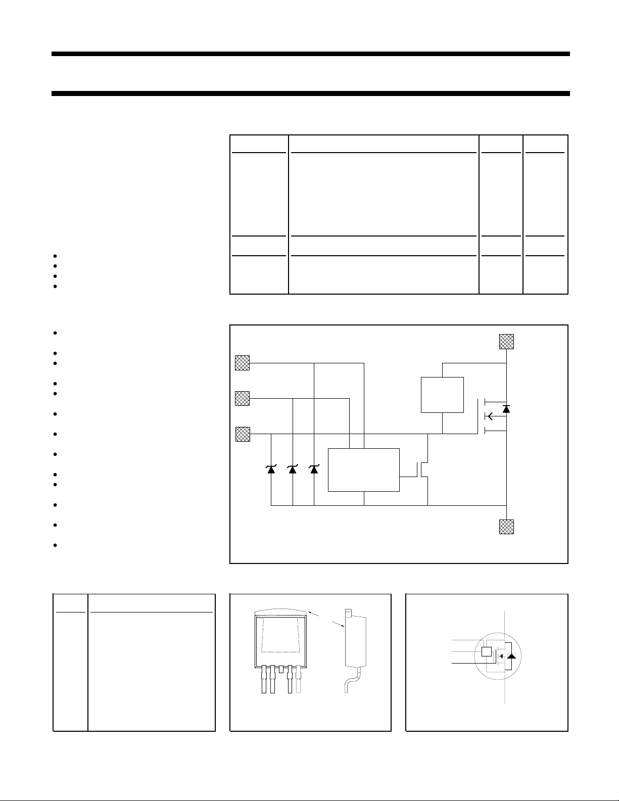
FEATURES FUNCTIONAL BLOCK DIAGRAM
Vertical power DMOS output
stage
Low on-state resistance
Logic and protection supply
from separate pin
Low operating supply current
Overload protection against
over temperature
Overload protection against
short circuit load
Latched overload protection
reset by protection supply
Protection circuit condition
indicated by flag pin
5 V logic compatible input level
Separate input pin
for higher frequency drive
ESD protection on input, flag
and protection supply pins
Over voltage clamping for turn
off of inductive loads
Both linear and switching
operation are possible Fig.1. Elements of the TOPFET.
PROTECTION SUPPLY
FLAG
INPUT
Continuous drain source voltage 50 V
Continuous drain current 15 A
Total power dissipation 40 W
Continuous junction temperature 150 ˚C
Drain-source on-state resistance
VIS = 5 V 125 mΩ
= 7 V 100 mΩ
IS
Protection supply voltage
DRAIN
O/V
CLAMP
LOGIC AND
PROTECTION
POWER
MOSFET
SOURCE
PINNING - SOT426 PIN CONFIGURATION SYMBOL
PIN DESCRIPTION
1 input
2 flag
3 (connected to mb)
4 protection supply
5 source
3
12 45
mb
TOPFET
P
F
I
Fig. 2. Fig. 3.
mb drain
September 1996 1 Rev 1.000
D
P
S

Philips Semiconductors Product specification
Logic level TOPFET BUK114-50L/S
SMD version of BUK104-50L/S
LIMITING VALUES
Limiting values in accordance with the Absolute Maximum Rating System (IEC 134)
SYMBOL PARAMETER CONDITIONS MIN. MAX. UNIT
V
V
V
V
I
D
I
D
I
DRM
P
T
T
T
DSS
IS
FS
PS
tot
stg
j
sold
Voltages
Continuous off-state drain source VIS = 0 V - 50 V
voltage
1
Continuous input voltage - 0 11 V
Continuous flag voltage - 0 11 V
Continuous supply voltage - 0 11 V
Currents VIS = - 7 5 V
Continuous drain current T
Continuous drain current T
Repetitive peak on-state drain current Tmb ≤ 25 ˚C - 60 54 A
25 ˚C - 15 13 A
mb ≤
100 ˚C - 9.5 8.5 A
mb ≤
Thermal
Total power dissipation Tmb = 25 ˚C - 40 W
Storage temperature - -55 150 ˚C
Junction temperature
2
continuous - 150 ˚C
Lead temperature during soldering - 250 ˚C
OVERLOAD PROTECTION LIMITING VALUES
With the protection supply An n-MOS transistor turns on For internal overload protection to
connected, TOPFET can protect between the input and source to remain latched while the control
itself from two types of overload - quickly discharge the power circuit is high, external series input
over temperature and short circuit MOSFET gate capacitance. resistance must be provided. Refer
load. to INPUT CHARACTERISTICS.
SYMBOL PARAMETER CONDITIONS MIN. MAX. UNIT
VIS =75 - V
V
PSP
Protection supply voltage
3
for valid protection
BUK114-50L 4.4 4 - V
BUK114-50S 5.4 5 - V
V
DDP(T)
V
DDP(P)
P
DSM
Over temperature protection VPS = V
Protected drain source supply voltage VIS = 10 V; RI ≥ 2 kΩ -50V
V
Short circuit load protection VPS = V
Protected drain source supply voltage4VIS = 10 V; RI ≥ 2 kΩ -25V
V
Instantaneous overload dissipation - 0.8 kW
PSN
= 5 V; RI ≥ 1 kΩ -50V
IS
; L ≤ 10 µH
PSN
= 5 V; RI ≥ 1 kΩ -45V
IS
ESD LIMITING VALUE
SYMBOL PARAMETER CONDITIONS MIN. MAX. UNIT
V
C
Electrostatic discharge capacitor Human body model; - 2 kV
voltage C = 250 pF; R = 1.5 kΩ
1 Prior to the onset of overvoltage clamping. For voltages above this value, safe operation is limited by the overvoltage clamping energy.
2 A higher Tj is allowed as an overload condition but at the threshold T
3 The minimum supply voltage required for correct operation of the overload protection circuits.
4 The device is able to self-protect against a short circuit load providing the drain-source supply voltage does not exceed V
For further information, refer to OVERLOAD PROTECTION CHARACTERISTICS.
the over temperature trip operates to protect the switch.
j(TO)
DDP(P)
maximum.
September 1996 2 Rev 1.000

Philips Semiconductors Product specification
Logic level TOPFET BUK114-50L/S
SMD version of BUK104-50L/S
OVERVOLTAGE CLAMPING LIMITING VALUES
At a drain source voltage above 50 V the power MOSFET is actively turned on to clamp overvoltage transients.
SYMBOL PARAMETER CONDITIONS MIN. MAX. UNIT
I
DRRM
E
DSM
E
DRM
Repetitive peak clamping drain current RIS ≥ 100 Ω
Non-repetitive inductive turn-off IDM = 15 A; RIS ≥ 100 Ω - 200 mJ
energy
2
Repetitive inductive turn-off energy RIS ≥ 100 Ω; Tmb ≤ 95 ˚C; - 20 mJ
IDM = 4 A; VDD ≤ 20 V;
f = 250 Hz
I
DIRM
Repetitive peak drain to input current3RIS = 0 Ω; tp ≤ 1 ms - 50 mA
REVERSE DIODE LIMITING VALUE
SYMBOL PARAMETER CONDITIONS MIN. MAX. UNIT
I
S
Continuous forward current Tmb = 25 ˚C; - 15 A
VIS = VPS = VFS = 0 V
THERMAL CHARACTERISTIC
1
-15A
SYMBOL PARAMETER CONDITIONS MIN. TYP. MAX. UNIT
Thermal resistance
R
th j-mb
Junction to mounting base - - 2.5 3.1 K/W
STATIC CHARACTERISTICS
Tmb = 25 ˚C unless otherwise specified
SYMBOL PARAMETER CONDITIONS MIN. TYP. MAX. UNIT
V
(CL)DSR
V
(CL)DSR
I
DSS
I
DSR
I
DSR
R
DS(ON)
Drain-source clamping voltage RIS = 100 Ω; ID = 10 mA 50 - 65 V
Drain-source clamping voltage RIS = 100 Ω; IDM = 1 A; tp ≤ 300 µs; 50 - 70 V
δ ≤ 0.01
Zero input voltage drain current VDS = 12 V; VIS = 0 V - 0.5 10 µA
Drain source leakage current VDS = 50 V; RIS = 100 Ω;-120µA
Drain source leakage current VDS = 40 V; RIS = 100 Ω;
Tj = 125 ˚C - 10 100 µA
Drain-source on-state IDM = 7.5 A; VIS = 7 V - 75 100 mΩ
resistance tp ≤ 300 µs; δ ≤ 0.01 VIS = 5 V - 95 125 mΩ
1 The input pin must be connected to the source pin by a specified external resistance to allow the power MOSFET gate source voltage to
2 While the protection supply voltage is connected, during overvoltage clamping it is possible that the overload protection may operate at
3 Shorting the input to source with low resistance inhibits the internal overvoltage protection by preventing the power MOSFET gate source
become sufficiently positive for active clamping. Refer to INPUT CHARACTERISTICS.
energies close to the limiting value. Refer to OVERLOAD PROTECTION CHARACTERISTICS.
voltage becoming positive.
September 1996 3 Rev 1.000

Philips Semiconductors Product specification
Logic level TOPFET BUK114-50L/S
SMD version of BUK104-50L/S
OVERLOAD PROTECTION CHARACTERISTICS
With adequate protection supply Provided there is adequate input Refer also to OVERLOAD
voltage TOPFET detects when one series resistance it switches off PROTECTION LIMITING VALUES
of the overload thresholds is and remains latched off until reset and INPUT CHARACTERISTICS.
exceeded. by the protection supply pin.
SYMBOL PARAMETER CONDITIONS MIN. TYP. MAX. UNIT
Short circuit load protection1VPS = V
RI ≥ 2 kΩ
E
t
d sc
DS(TO)
Overload threshold energy VDD = 13 V; VIS = 10 V - 150 - mJ
Response time VDD = 13 V; VIS = 10 V - 375 - µs
Over temperature protection VPS = V
T
j(TO)
Threshold junction temperature from ID ≥ 0.65 A
TRANSFER CHARACTERISTICS
Tmb = 25 ˚C
SYMBOL PARAMETER CONDITIONS MIN. TYP. MAX. UNIT
g
fs
I
D
Forward transconductance VDS = 10 V; IDM = 7.5 A tp ≤ 300 µs; 5 9 - S
δ ≤ 0.01
Drain current
4
VDS = 13 V; VIS = 5 V - 25 - A
2
; Tmb = 25 ˚C; L ≤ 10 µH;
PSN
; RI ≥ 2 kΩ
PSN
3
VIS = 10 V 40 - A
150 - - ˚C
PROTECTION SUPPLY CHARACTERISTICS
Tmb = 25 ˚C unless otherwise specified
SYMBOL PARAMETER CONDITIONS MIN. TYP. MAX. UNIT
Protection supply
IPS, Protection supply current normal operation or
I
PSL
protection latched
BUK114-50L VPS = 5 V - 0.2 0.35 mA
V
PSR
Protection reset voltage
5
BUK114-50S VPS = 10 V - 0.4 1.0 mA
1.5 2.5 3.5 V
Tj = 150 ˚C 1.0 - - V
V
(CL)PS
Protection clamp voltage IP = 1.35 mA 11 13 - V
REVERSE DIODE CHARACTERISTICS
Tmb = 25 ˚C
SYMBOL PARAMETER CONDITIONS MIN. TYP. MAX. UNIT
V
SDS
t
rr
1 The short circuit load protection is able to save the device providing the instantaneous on-state dissipation is less than the limiting value for
2 At the appropriate nominal protection supply voltage for each type. Refer to QUICK REFERENCE DATA.
3 The over temperature protection feature requires a minimum on-state drain source voltage for correct operation. The specified minimum I
4 During overload condition. Refer also to OVERLOAD PROTECTION LIMITING VALUES and CHARACTERISTICS.
5 The supply voltage below which the overload protection circuits will be reset.
6 The reverse diode of this type is not intended for applications requiring fast reverse recovery.
Forward voltage IS = 15 A; VIS = VPS = VFS = 0 V; - 1.0 1.5 V
tp = 300 µs
Reverse recovery time not applicable
P
, which is always the case when VDS is less than V
DSM
ensures this condition.
maximum.
DSP
6
----
D
September 1996 4 Rev 1.000
 Loading...